STM32F030x4-STM32F030x6-STM32F030x8 - STMicroelectronics - Farnell Element 14
- Revenir à l'accueil


")

Farnell Element 14 :


See the trailer for the next exciting episode of The Ben Heck show. Check back on Friday to be among the first to see the exclusive full show on element…

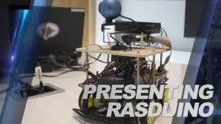
Connect your Raspberry Pi to a breadboard, download some code and create a push-button audio play project.


Puce électronique / Microchip :


Sans fil - Wireless :


Texas instrument :


Ordinateurs :


Logiciels :


Tutoriels :


Autres documentations :
![[TXT]](http://www.audentia-gestion.fr/icons/text.gif)
Analog-Devices-ADC-S..> 09-Sep-2014 08:21 2.4M
Analog-Devices-ADMC2..> 09-Sep-2014 08:21 2.4M
Analog-Devices-ADMC4..> 09-Sep-2014 08:23 2.3M
Analog-Devices-AN300..> 08-Sep-2014 17:42 2.0M
Analog-Devices-ANF32..> 09-Sep-2014 08:18 2.6M
Analog-Devices-Basic..> 08-Sep-2014 17:49 1.9M
Analog-Devices-Compl..> 08-Sep-2014 17:38 2.0M
Analog-Devices-Convo..> 09-Sep-2014 08:26 2.1M
Analog-Devices-Convo..> 09-Sep-2014 08:25 2.2M
Analog-Devices-Convo..> 09-Sep-2014 08:25 2.2M
Analog-Devices-Digit..> 08-Sep-2014 18:02 2.1M
Analog-Devices-Digit..> 08-Sep-2014 18:03 2.0M
Analog-Devices-Gloss..> 08-Sep-2014 17:36 2.0M
Analog-Devices-Intro..> 08-Sep-2014 17:39 1.9M
Analog-Devices-The-C..> 08-Sep-2014 17:41 1.9M
Analog-Devices-Visua..> 09-Sep-2014 08:18 2.5M
Analog-Devices-Wi-Fi..> 09-Sep-2014 08:23 2.3M
Electronique-Basic-o..> 08-Sep-2014 17:43 1.8M
Farnell-0050375063-D..> 18-Jul-2014 17:03 2.5M
Farnell-03-iec-runds..> 04-Jul-2014 10:40 3.7M
Farnell-0430300011-D..> 14-Jun-2014 18:13 2.0M
Farnell-0433751001-D..> 18-Jul-2014 17:02 2.5M
Farnell-06-6544-8-PD..> 26-Mar-2014 17:56 2.7M
Farnell-1N4148WS-Fai..> 06-Jul-2014 10:04 1.9M
Farnell-2-GBPS-Diffe..> 28-Jul-2014 17:42 2.7M
Farnell-2N3906-Fairc..> 08-Sep-2014 07:22 2.1M
Farnell-2N7002DW-Fai..> 06-Jul-2014 10:03 886K
Farnell-3M-Polyimide..> 21-Mar-2014 08:09 3.9M
Farnell-3M-VolitionT..> 25-Mar-2014 08:18 3.3M
Farnell-4-Bit-Magnit..> 08-Jul-2014 18:53 2.2M
Farnell-10BQ060-PDF.htm 14-Jun-2014 09:50 2.4M
Farnell-10TPB47M-End..> 14-Jun-2014 18:16 3.4M
Farnell-12mm-Size-In..> 14-Jun-2014 09:50 2.4M
Farnell-24AA024-24LC..> 23-Jun-2014 10:26 3.1M
Farnell-50A-High-Pow..> 20-Mar-2014 17:31 2.9M
Farnell-74AC00-74ACT..> 06-Jul-2014 10:03 911K
Farnell-74LCX573-Fai..> 06-Jul-2014 10:05 1.9M
Farnell-197.31-KB-Te..> 04-Jul-2014 10:42 3.3M
Farnell-270-Series-O..> 08-Jul-2014 18:49 2.3M
Farnell-760G-French-..> 07-Jul-2014 19:45 1.2M
Farnell-851-Series-P..> 08-Jul-2014 18:47 3.0M
Farnell-900-Series-B..> 08-Jul-2014 18:50 2.3M
Farnell-1734-ARALDIT..> 07-Jul-2014 19:45 1.2M
Farnell-1907-2006-PD..> 26-Mar-2014 17:56 2.7M
Farnell-2020-Manuel-..> 08-Jul-2014 18:55 2.1M
Farnell-3367-ARALDIT..> 07-Jul-2014 19:46 1.2M
Farnell-5910-PDF.htm 25-Mar-2014 08:15 3.0M
Farnell-6517b-Electr..> 29-Mar-2014 11:12 3.3M
Farnell-43031-0002-M..> 18-Jul-2014 17:03 2.5M
Farnell-A-4-Hardener..> 07-Jul-2014 19:44 1.4M
Farnell-A-True-Syste..> 29-Mar-2014 11:13 3.3M
Farnell-AC-DC-Power-..> 15-Jul-2014 16:47 845K
Farnell-ACC-Silicone..> 04-Jul-2014 10:40 3.7M
Farnell-AD524-PDF.htm 20-Mar-2014 17:33 2.8M
Farnell-AD584-Rev-C-..> 08-Sep-2014 07:20 2.2M
Farnell-AD586BRZ-Ana..> 08-Sep-2014 08:09 1.6M
Farnell-AD620-Rev-H-..> 09-Sep-2014 08:13 2.6M
Farnell-AD736-Rev-I-..> 08-Sep-2014 07:31 1.3M
Farnell-AD7171-16-Bi..> 06-Jul-2014 10:06 1.0M
Farnell-AD7719-Low-V..> 18-Jul-2014 16:59 1.4M
Farnell-AD8300-Data-..> 18-Jul-2014 16:56 1.3M
Farnell-AD8307-Data-..> 08-Sep-2014 07:30 1.3M
Farnell-AD8310-Analo..> 08-Sep-2014 07:24 2.1M
Farnell-AD8313-Analo..> 08-Sep-2014 07:26 2.0M
Farnell-AD8361-Rev-D..> 08-Sep-2014 07:23 2.1M
Farnell-AD9833-Rev-E..> 08-Sep-2014 17:49 1.8M
Farnell-AD9834-Rev-D..> 08-Sep-2014 07:32 1.2M
Farnell-ADE7753-Rev-..> 08-Sep-2014 07:20 2.3M
Farnell-ADE7758-Rev-..> 08-Sep-2014 07:28 1.7M
Farnell-ADL6507-PDF.htm 14-Jun-2014 18:19 3.4M
Farnell-ADSP-21362-A..> 20-Mar-2014 17:34 2.8M
Farnell-ADuM1200-ADu..> 08-Sep-2014 08:09 1.6M
Farnell-ADuM1300-ADu..> 08-Sep-2014 08:11 1.7M
Farnell-ALF1210-PDF.htm 06-Jul-2014 10:06 4.0M
Farnell-ALF1225-12-V..> 01-Apr-2014 07:40 3.4M
Farnell-ALF2412-24-V..> 01-Apr-2014 07:39 3.4M
Farnell-AN10361-Phil..> 23-Jun-2014 10:29 2.1M
Farnell-ARADUR-HY-13..> 26-Mar-2014 17:55 2.8M
Farnell-ARALDITE-201..> 21-Mar-2014 08:12 3.7M
Farnell-ARALDITE-CW-..> 26-Mar-2014 17:56 2.7M
Farnell-AT89C5131-Ha..> 29-Jul-2014 10:31 1.2M
Farnell-AT90USBKey-H..> 29-Jul-2014 10:31 902K
Farnell-ATMEL-8-bit-..> 19-Mar-2014 18:04 2.1M
Farnell-ATMEL-8-bit-..> 11-Mar-2014 07:55 2.1M
Farnell-ATmega640-VA..> 14-Jun-2014 09:49 2.5M
Farnell-ATtiny20-PDF..> 25-Mar-2014 08:19 3.6M
Farnell-ATtiny26-L-A..> 18-Jul-2014 17:00 2.6M
Farnell-ATtiny26-L-A..> 13-Jun-2014 18:40 1.8M
Farnell-Alimentation..> 07-Jul-2014 19:43 1.8M
Farnell-Alimentation..> 14-Jun-2014 18:24 2.5M
Farnell-Alimentation..> 01-Apr-2014 07:42 3.4M
Farnell-Amplificateu..> 29-Mar-2014 11:11 3.3M
Farnell-Amplifier-In..> 06-Jul-2014 10:02 940K
Farnell-An-Improved-..> 14-Jun-2014 09:49 2.5M
Farnell-Araldite-Fus..> 07-Jul-2014 19:45 1.2M
Farnell-Arithmetic-L..> 08-Jul-2014 18:54 2.1M
Farnell-Atmel-ATmega..> 19-Mar-2014 18:03 2.2M
Farnell-Avvertenze-e..> 14-Jun-2014 18:20 3.3M
Farnell-BA-Series-Oh..> 08-Jul-2014 18:50 2.3M
Farnell-BAV99-Fairch..> 06-Jul-2014 10:03 896K
Farnell-BC846DS-NXP-..> 13-Jun-2014 18:42 1.6M
Farnell-BC847DS-NXP-..> 23-Jun-2014 10:24 3.3M
Farnell-BD6xxx-PDF.htm 22-Jul-2014 12:33 1.6M
Farnell-BF545A-BF545..> 23-Jun-2014 10:28 2.1M
Farnell-BGA7124-400-..> 18-Jul-2014 16:59 1.5M
Farnell-BK889B-PONT-..> 07-Jul-2014 19:42 1.8M
Farnell-BK2650A-BK26..> 29-Mar-2014 11:10 3.3M
Farnell-BT151-650R-N..> 13-Jun-2014 18:40 1.7M
Farnell-BTA204-800C-..> 13-Jun-2014 18:42 1.6M
Farnell-BUJD203AX-NX..> 13-Jun-2014 18:41 1.7M
Farnell-BYV29F-600-N..> 13-Jun-2014 18:42 1.6M
Farnell-BYV79E-serie..> 10-Mar-2014 16:19 1.6M
Farnell-BZX384-serie..> 23-Jun-2014 10:29 2.1M
Farnell-Battery-GBA-..> 14-Jun-2014 18:13 2.0M
Farnell-Both-the-Del..> 06-Jul-2014 10:01 948K
Farnell-C.A-6150-C.A..> 14-Jun-2014 18:24 2.5M
Farnell-C.A 8332B-C...> 01-Apr-2014 07:40 3.4M
Farnell-CC-Debugger-..> 07-Jul-2014 19:44 1.5M
Farnell-CC2530ZDK-Us..> 08-Jul-2014 18:55 2.1M
Farnell-CC2531-USB-H..> 07-Jul-2014 19:43 1.8M
Farnell-CC2560-Bluet..> 29-Mar-2014 11:14 2.8M
Farnell-CD4536B-Type..> 14-Jun-2014 18:13 2.0M
Farnell-CIRRUS-LOGIC..> 10-Mar-2014 17:20 2.1M
Farnell-CLASS 1-or-2..> 22-Jul-2014 12:30 4.7M
Farnell-CRC-HANDCLEA..> 07-Jul-2014 19:46 1.2M
Farnell-CS5532-34-BS..> 01-Apr-2014 07:39 3.5M
Farnell-Cannon-ZD-PD..> 11-Mar-2014 08:13 2.8M
Farnell-Ceramic-tran..> 14-Jun-2014 18:19 3.4M
Farnell-Circuit-Impr..> 25-Jul-2014 12:22 3.1M
Farnell-Circuit-Note..> 26-Mar-2014 18:00 2.8M
Farnell-Circuit-Note..> 26-Mar-2014 18:00 2.8M
Farnell-Cles-electro..> 21-Mar-2014 08:13 3.9M
Farnell-Clipper-Seri..> 08-Jul-2014 18:48 2.8M
Farnell-Compensating..> 09-Sep-2014 08:16 2.6M
Farnell-Compensating..> 09-Sep-2014 08:16 2.6M
Farnell-Conception-d..> 11-Mar-2014 07:49 2.4M
Farnell-Connectors-N..> 14-Jun-2014 18:12 2.1M
Farnell-Construction..> 14-Jun-2014 18:25 2.5M
Farnell-Controle-de-..> 11-Mar-2014 08:16 2.8M
Farnell-Cordless-dri..> 14-Jun-2014 18:13 2.0M
Farnell-Cube-3D-Prin..> 18-Jul-2014 17:02 2.5M
Farnell-Current-Tran..> 26-Mar-2014 17:58 2.7M
Farnell-Current-Tran..> 26-Mar-2014 17:58 2.7M
Farnell-Current-Tran..> 26-Mar-2014 17:59 2.7M
Farnell-Current-Tran..> 26-Mar-2014 17:59 2.7M
Farnell-DAC8143-Data..> 18-Jul-2014 16:59 1.5M
Farnell-DC-DC-Conver..> 15-Jul-2014 16:48 781K
Farnell-DC-Fan-type-..> 14-Jun-2014 09:48 2.5M
Farnell-DC-Fan-type-..> 14-Jun-2014 09:51 1.8M
Farnell-DG411-DG412-..> 07-Jul-2014 19:47 1.0M
Farnell-DP83846A-DsP..> 18-Jul-2014 16:55 1.5M
Farnell-DS3231-DS-PD..> 18-Jul-2014 16:57 2.5M
Farnell-Data-Sheet-K..> 07-Jul-2014 19:46 1.2M
Farnell-Data-Sheet-M..> 09-Sep-2014 08:05 2.8M
Farnell-Data-Sheet-S..> 18-Jul-2014 17:00 1.2M
Farnell-Datasheet-FT..> 09-Sep-2014 08:10 2.8M
Farnell-Datasheet-Fa..> 06-Jul-2014 10:04 861K
Farnell-Datasheet-Fa..> 15-Jul-2014 17:05 1.0M
Farnell-Datasheet-NX..> 15-Jul-2014 17:06 1.0M
Farnell-Davum-TMC-PD..> 14-Jun-2014 18:27 2.4M
Farnell-De-la-puissa..> 29-Mar-2014 11:10 3.3M
Farnell-Decapant-KF-..> 07-Jul-2014 19:45 1.2M
Farnell-Directive-re..> 25-Mar-2014 08:16 3.0M
Farnell-Documentatio..> 14-Jun-2014 18:26 2.5M
Farnell-Download-dat..> 16-Jul-2014 09:02 2.2M
Farnell-Download-dat..> 13-Jun-2014 18:40 1.8M
Farnell-Dremel-Exper..> 22-Jul-2014 12:34 1.6M
Farnell-Dual-MOSFET-..> 28-Jul-2014 17:41 2.8M
Farnell-ECO-Series-T..> 20-Mar-2014 08:14 2.5M
Farnell-EE-SPX303N-4..> 15-Jul-2014 17:06 969K
Farnell-ELMA-PDF.htm 29-Mar-2014 11:13 3.3M
Farnell-EMC1182-PDF.htm 25-Mar-2014 08:17 3.0M
Farnell-EPCOS-173438..> 04-Jul-2014 10:43 3.3M
Farnell-EPCOS-Sample..> 11-Mar-2014 07:53 2.2M
Farnell-ES1F-ES1J-fi..> 06-Jul-2014 10:04 867K
Farnell-ES2333-PDF.htm 11-Mar-2014 08:14 2.8M
Farnell-ESCON-Featur..> 06-Jul-2014 10:05 938K
Farnell-ESCON-Featur..> 06-Jul-2014 10:02 931K
Farnell-Ed.081002-DA..> 19-Mar-2014 18:02 2.5M
Farnell-Encodeur-USB..> 08-Jul-2014 18:56 2.0M
Farnell-Evaluating-t..> 22-Jul-2014 12:28 4.9M
Farnell-Everything-Y..> 11-Oct-2014 12:05 1.5M
Farnell-Excalibur-Hi..> 28-Jul-2014 17:10 2.4M
Farnell-Excalibur-Hi..> 28-Jul-2014 17:10 2.4M
Farnell-Explorer-16-..> 29-Jul-2014 10:31 1.3M
Farnell-F28069-Picco..> 14-Jun-2014 18:14 2.0M
Farnell-F42202-PDF.htm 19-Mar-2014 18:00 2.5M
Farnell-FAN6756-Fair..> 06-Jul-2014 10:04 850K
Farnell-FDC2512-Fair..> 06-Jul-2014 10:03 886K
Farnell-FDS-ITW-Spra..> 14-Jun-2014 18:22 3.3M
Farnell-FDV301N-Digi..> 06-Jul-2014 10:03 886K
Farnell-FICHE-DE-DON..> 10-Mar-2014 16:17 1.6M
Farnell-Fast-Charge-..> 28-Jul-2014 17:12 6.4M
Farnell-Fastrack-Sup..> 23-Jun-2014 10:25 3.3M
Farnell-Ferric-Chlor..> 29-Mar-2014 11:14 2.8M
Farnell-Fiche-de-don..> 14-Jun-2014 09:47 2.5M
Farnell-Fiche-de-don..> 14-Jun-2014 18:26 2.5M
Farnell-Fluke-1730-E..> 14-Jun-2014 18:23 2.5M
Farnell-Full-Datashe..> 15-Jul-2014 17:08 951K
Farnell-Full-Datashe..> 15-Jul-2014 16:47 803K
Farnell-GALVA-A-FROI..> 26-Mar-2014 17:56 2.7M
Farnell-GALVA-MAT-Re..> 26-Mar-2014 17:57 2.7M
Farnell-GN-RELAYS-AG..> 20-Mar-2014 08:11 2.6M
Farnell-Gertboard-Us..> 29-Jul-2014 10:30 1.4M
Farnell-HC49-4H-Crys..> 14-Jun-2014 18:20 3.3M
Farnell-HFE1600-Data..> 14-Jun-2014 18:22 3.3M
Farnell-HI-70300-Sol..> 14-Jun-2014 18:27 2.4M
Farnell-HIP4081A-Int..> 07-Jul-2014 19:47 1.0M
Farnell-HUNTSMAN-Adv..> 10-Mar-2014 16:17 1.7M
Farnell-Haute-vitess..> 11-Mar-2014 08:17 2.4M
Farnell-Hex-Inverter..> 29-Jul-2014 10:31 875K
Farnell-High-precisi..> 08-Jul-2014 18:51 2.3M
Farnell-ICM7228-Inte..> 07-Jul-2014 19:46 1.1M
Farnell-IP4252CZ16-8..> 13-Jun-2014 18:41 1.7M
Farnell-ISL6251-ISL6..> 07-Jul-2014 19:47 1.1M
Farnell-Instructions..> 19-Mar-2014 18:01 2.5M
Farnell-Jeu-multi-la..> 25-Jul-2014 12:23 3.0M
Farnell-KSZ8851SNL-S..> 23-Jun-2014 10:28 2.1M
Farnell-Keyboard-Mou..> 22-Jul-2014 12:27 5.9M
Farnell-L-efficacite..> 11-Mar-2014 07:52 2.3M
Farnell-L78S-STMicro..> 22-Jul-2014 12:32 1.6M
Farnell-L293d-Texas-..> 08-Jul-2014 18:53 2.2M
Farnell-LCW-CQ7P.CC-..> 25-Mar-2014 08:19 3.2M
Farnell-LD-WSECO16-P..> 25-Jul-2014 12:22 3.1M
Farnell-LM3S6952-Mic..> 22-Jul-2014 12:27 5.9M
Farnell-LM19-Texas-I..> 18-Jul-2014 17:00 1.2M
Farnell-LM324-Texas-..> 29-Jul-2014 10:32 1.5M
Farnell-LM386-Low-Vo..> 29-Jul-2014 10:32 1.5M
Farnell-LM555-Timer-..> 08-Jul-2014 18:53 2.2M
Farnell-LM7805-Fairc..> 09-Sep-2014 08:13 2.7M
Farnell-LME49725-Pow..> 14-Jun-2014 09:49 2.5M
Farnell-LMH6518-Texa..> 18-Jul-2014 16:59 1.3M
Farnell-LMP91051-Use..> 29-Jul-2014 10:30 1.4M
Farnell-LMT88-2.4V-1..> 28-Jul-2014 17:42 2.8M
Farnell-LOCTITE-542-..> 25-Mar-2014 08:15 3.0M
Farnell-LOCTITE-3463..> 25-Mar-2014 08:19 3.0M
Farnell-LPC11U3x-32-..> 16-Jul-2014 09:01 2.4M
Farnell-LPC81xM-32-b..> 16-Jul-2014 09:02 2.0M
Farnell-LPC408x-7x 3..> 16-Jul-2014 09:03 1.6M
Farnell-LPC1769-68-6..> 16-Jul-2014 09:02 1.9M
Farnell-LPC3220-30-4..> 16-Jul-2014 09:02 2.2M
Farnell-LQ-RELAYS-AL..> 06-Jul-2014 10:02 924K
Farnell-LT1961-Linea..> 18-Jul-2014 16:58 1.6M
Farnell-LT3757-Linea..> 18-Jul-2014 16:58 1.6M
Farnell-LT6233-Linea..> 18-Jul-2014 16:56 1.3M
Farnell-LUMINARY-MIC..> 22-Jul-2014 12:31 3.6M
Farnell-LUXEON-Guide..> 11-Mar-2014 07:52 2.3M
Farnell-Leaded-Trans..> 23-Jun-2014 10:26 3.2M
Farnell-Les-derniers..> 11-Mar-2014 07:50 2.3M
Farnell-Loctite3455-..> 25-Mar-2014 08:16 3.0M
Farnell-Low-Noise-24..> 06-Jul-2014 10:05 1.0M
Farnell-Low-cost-Enc..> 13-Jun-2014 18:42 1.7M
Farnell-Lubrifiant-a..> 26-Mar-2014 18:00 2.7M
Farnell-MAX232-MAX23..> 08-Jul-2014 18:52 2.3M
Farnell-MAX1365-MAX1..> 18-Jul-2014 16:56 1.4M
Farnell-MAX3221-Rev-..> 08-Sep-2014 07:28 1.8M
Farnell-MAX4661-MAX4..> 09-Sep-2014 08:10 2.8M
Farnell-MC3510-PDF.htm 25-Mar-2014 08:17 3.0M
Farnell-MC21605-PDF.htm 11-Mar-2014 08:14 2.8M
Farnell-MCF532x-7x-E..> 29-Mar-2014 11:14 2.8M
Farnell-MCOC1-Farnel..> 16-Jul-2014 09:04 1.0M
Farnell-MCP3421-Micr..> 18-Jul-2014 17:00 1.2M
Farnell-MICREL-KSZ88..> 11-Mar-2014 07:54 2.2M
Farnell-MICROCHIP-PI..> 19-Mar-2014 18:02 2.5M
Farnell-MICROCHIP-PI..> 25-Jul-2014 12:34 6.7M
Farnell-MIDAS-un-tra..> 15-Jul-2014 17:05 1.0M
Farnell-MOLEX-39-00-..> 10-Mar-2014 17:19 1.9M
Farnell-MOLEX-43020-..> 10-Mar-2014 17:21 1.9M
Farnell-MOLEX-43160-..> 10-Mar-2014 17:21 1.9M
Farnell-MOLEX-87439-..> 10-Mar-2014 17:21 1.9M
Farnell-MPXV7002-Rev..> 20-Mar-2014 17:33 2.8M
Farnell-MSP-EXP430F5..> 29-Jul-2014 10:31 1.2M
Farnell-MSP430-Hardw..> 29-Jul-2014 10:36 1.1M
Farnell-MSP430F15x-M..> 08-Sep-2014 07:32 1.3M
Farnell-MTX-3250-MTX..> 18-Jul-2014 17:01 2.5M
Farnell-MTX-Compact-..> 18-Jul-2014 17:01 2.5M
Farnell-MULTICOMP-Ra..> 22-Jul-2014 12:57 5.9M
Farnell-MX670-MX675-..> 14-Jun-2014 09:46 2.5M
Farnell-Microchip-MC..> 13-Jun-2014 18:27 1.8M
Farnell-Microship-PI..> 11-Mar-2014 07:53 2.2M
Farnell-Midas-Active..> 14-Jun-2014 18:17 3.4M
Farnell-Midas-MCCOG4..> 14-Jun-2014 18:11 2.1M
Farnell-Mini-Fit-Jr-..> 18-Jul-2014 17:03 2.5M
Farnell-Miniature-Ci..> 26-Mar-2014 17:55 2.8M
Farnell-Mistral-PDF.htm 14-Jun-2014 18:12 2.1M
Farnell-Molex-83421-..> 14-Jun-2014 18:17 3.4M
Farnell-Molex-COMMER..> 14-Jun-2014 18:16 3.4M
Farnell-Molex-Crimp-..> 10-Mar-2014 16:27 1.7M
Farnell-Multi-Functi..> 20-Mar-2014 17:38 3.0M
Farnell-NA555-NE555-..> 08-Jul-2014 18:53 2.2M
Farnell-NA555-NE555-..> 08-Sep-2014 07:51 1.5M
Farnell-NE5532-Texas..> 29-Jul-2014 10:32 1.5M
Farnell-NTE_SEMICOND..> 11-Mar-2014 07:52 2.3M
Farnell-NVE-datashee..> 28-Jul-2014 17:12 6.5M
Farnell-NXP-74VHC126..> 10-Mar-2014 16:17 1.6M
Farnell-NXP-BT136-60..> 11-Mar-2014 07:52 2.3M
Farnell-NXP-PBSS9110..> 10-Mar-2014 17:21 1.9M
Farnell-NXP-PCA9555 ..> 11-Mar-2014 07:54 2.2M
Farnell-NXP-PMBFJ620..> 10-Mar-2014 16:16 1.7M
Farnell-NXP-PSMN1R7-..> 10-Mar-2014 16:17 1.6M
Farnell-NXP-PSMN7R0-..> 10-Mar-2014 17:19 2.1M
Farnell-NXP-TEA1703T..> 11-Mar-2014 08:15 2.8M
Farnell-NaPiOn-Panas..> 06-Jul-2014 10:02 911K
Farnell-Nilï¬-sk-E-..> 14-Jun-2014 09:47 2.5M
Farnell-Novembre-201..> 20-Mar-2014 17:38 3.3M
Farnell-OMRON-INDUST..> 25-Jul-2014 12:31 6.9M
Farnell-OMRON-INDUST..> 25-Jul-2014 12:32 6.9M
Farnell-OMRON-Master..> 10-Mar-2014 16:26 1.8M
Farnell-OPA627-Texas..> 09-Sep-2014 08:08 2.8M
Farnell-OSLON-SSL-Ce..> 19-Mar-2014 18:03 2.1M
Farnell-OXPCIE958-FB..> 13-Jun-2014 18:40 1.8M
Farnell-Octal-Genera..> 28-Jul-2014 17:42 2.8M
Farnell-PADO-semi-au..> 04-Jul-2014 10:41 3.7M
Farnell-PBSS5160T-60..> 19-Mar-2014 18:03 2.1M
Farnell-PCF8574-PCF8..> 16-Jul-2014 09:03 1.7M
Farnell-PDTA143X-ser..> 20-Mar-2014 08:12 2.6M
Farnell-PDTB123TT-NX..> 13-Jun-2014 18:43 1.5M
Farnell-PESD5V0F1BL-..> 13-Jun-2014 18:43 1.5M
Farnell-PESD9X5.0L-P..> 13-Jun-2014 18:43 1.6M
Farnell-PIC12F609-61..> 04-Jul-2014 10:41 3.7M
Farnell-PIC18F2420-2..> 18-Jul-2014 16:57 2.5M
Farnell-PIC18F2455-2..> 23-Jun-2014 10:27 3.1M
Farnell-PIC24FJ256GB..> 14-Jun-2014 09:51 2.4M
Farnell-PMBT3906-PNP..> 13-Jun-2014 18:44 1.5M
Farnell-PMBT4403-PNP..> 23-Jun-2014 10:27 3.1M
Farnell-PMEG4002EL-N..> 14-Jun-2014 18:18 3.4M
Farnell-PMEG4010CEH-..> 13-Jun-2014 18:43 1.6M
Farnell-PN512-Full-N..> 16-Jul-2014 09:03 1.4M
Farnell-Panasonic-15..> 23-Jun-2014 10:29 2.1M
Farnell-Panasonic-EC..> 20-Mar-2014 17:36 2.6M
Farnell-Panasonic-EZ..> 20-Mar-2014 08:10 2.6M
Farnell-Panasonic-Id..> 20-Mar-2014 17:35 2.6M
Farnell-Panasonic-Ne..> 20-Mar-2014 17:36 2.6M
Farnell-Panasonic-Ra..> 20-Mar-2014 17:37 2.6M
Farnell-Panasonic-TS..> 20-Mar-2014 08:12 2.6M
Farnell-Panasonic-Y3..> 20-Mar-2014 08:11 2.6M
Farnell-PiFace-Digit..> 25-Jul-2014 12:25 3.0M
Farnell-Pico-Spox-Wi..> 10-Mar-2014 16:16 1.7M
Farnell-PicoScope-42..> 25-Jul-2014 12:23 3.0M
Farnell-PicoScope-se..> 25-Jul-2014 12:24 3.0M
Farnell-Pompes-Charg..> 24-Apr-2014 20:23 3.3M
Farnell-Ponts-RLC-po..> 14-Jun-2014 18:23 3.3M
Farnell-Portable-Ana..> 29-Mar-2014 11:16 2.8M
Farnell-Power-suppli..> 25-Jul-2014 12:29 7.0M
Farnell-Premier-Farn..> 21-Mar-2014 08:11 3.8M
Farnell-Produit-3430..> 14-Jun-2014 09:48 2.5M
Farnell-Proskit-SS-3..> 10-Mar-2014 16:26 1.8M
Farnell-Puissance-ut..> 11-Mar-2014 07:49 2.4M
Farnell-Q48-PDF.htm 23-Jun-2014 10:29 2.1M
Farnell-QRE1113-Fair..> 06-Jul-2014 10:03 879K
Farnell-Quadruple-2-..> 08-Sep-2014 07:29 1.5M
Farnell-Quick-Start-..> 25-Jul-2014 12:25 3.0M
Farnell-RASPBERRY-PI..> 22-Jul-2014 12:35 5.9M
Farnell-RDS-80-PDF.htm 18-Jul-2014 16:57 1.3M
Farnell-REF19x-Serie..> 09-Sep-2014 08:08 2.8M
Farnell-REF102-10V-P..> 28-Jul-2014 17:09 2.4M
Farnell-RF-short-tra..> 28-Jul-2014 17:16 6.3M
Farnell-Radial-Lead-..> 20-Mar-2014 08:12 2.6M
Farnell-RaspiCam-Doc..> 22-Jul-2014 12:32 1.6M
Farnell-Realiser-un-..> 11-Mar-2014 07:51 2.3M
Farnell-Reglement-RE..> 21-Mar-2014 08:08 3.9M
Farnell-Repartiteurs..> 14-Jun-2014 18:26 2.5M
Farnell-S-TRI-SWT860..> 21-Mar-2014 08:11 3.8M
Farnell-S1A-Fairchil..> 06-Jul-2014 10:03 896K
Farnell-SB175-Connec..> 11-Mar-2014 08:14 2.8M
Farnell-SB520-SB5100..> 22-Jul-2014 12:32 1.6M
Farnell-SERIAL-TFT-M..> 15-Jul-2014 17:05 1.0M
Farnell-SICK-OPTIC-E..> 18-Jul-2014 16:58 1.5M
Farnell-SL3ICS1002-1..> 16-Jul-2014 09:05 2.5M
Farnell-SL3S1203_121..> 16-Jul-2014 09:04 1.1M
Farnell-SL3S4011_402..> 16-Jul-2014 09:03 1.1M
Farnell-SL59830-Inte..> 06-Jul-2014 10:11 1.0M
Farnell-SMBJ-Transil..> 29-Mar-2014 11:12 3.3M
Farnell-SMU-Instrume..> 08-Jul-2014 18:51 2.3M
Farnell-SN54HC164-SN..> 08-Sep-2014 07:25 2.0M
Farnell-SN54HC244-SN..> 08-Jul-2014 18:52 2.3M
Farnell-SN54LV4053A-..> 28-Jul-2014 17:20 5.9M
Farnell-SO967460-PDF..> 11-Oct-2014 12:05 2.9M
Farnell-SOT-23-Multi..> 11-Mar-2014 07:51 2.3M
Farnell-SOURIAU-Cont..> 08-Jul-2014 19:04 3.0M
Farnell-SPLC780A1-16..> 14-Jun-2014 18:25 2.5M
Farnell-SSC7102-Micr..> 23-Jun-2014 10:25 3.2M
Farnell-STM32F103x8-..> 22-Jul-2014 12:33 1.6M
Farnell-STM32F405xxS..> 27-Aug-2014 18:27 1.8M
Farnell-SVPE-series-..> 14-Jun-2014 18:15 2.0M
Farnell-Schroff-A108..> 25-Jul-2014 12:27 2.8M
Farnell-Schroff-Main..> 25-Jul-2014 12:26 2.9M
Farnell-Schroff-mult..> 25-Jul-2014 12:26 2.9M
Farnell-Sensorless-C..> 04-Jul-2014 10:42 3.3M
Farnell-Septembre-20..> 20-Mar-2014 17:46 3.7M
Farnell-Serial-File-..> 06-Jul-2014 10:02 941K
Farnell-Serie-PicoSc..> 19-Mar-2014 18:01 2.5M
Farnell-Serie-Standa..> 14-Jun-2014 18:23 3.3M
Farnell-Series-2600B..> 20-Mar-2014 17:30 3.0M
Farnell-Series-TDS10..> 04-Jul-2014 10:39 4.0M
Farnell-Signal-PCB-R..> 14-Jun-2014 18:11 2.1M
Farnell-Silica-Gel-M..> 07-Jul-2014 19:46 1.2M
Farnell-Single-Chip-..> 08-Sep-2014 07:30 1.5M
Farnell-SmartRF06-Ev..> 07-Jul-2014 19:43 1.6M
Farnell-Strangkuhlko..> 21-Mar-2014 08:09 3.9M
Farnell-Supercapacit..> 26-Mar-2014 17:57 2.7M
Farnell-Synchronous-..> 08-Jul-2014 18:54 2.1M
Farnell-T672-3000-Se..> 08-Jul-2014 18:59 2.0M
Farnell-TAS1020B-USB..> 28-Jul-2014 17:19 6.2M
Farnell-TCL-DC-traco..> 15-Jul-2014 16:46 858K
Farnell-TDK-Lambda-H..> 14-Jun-2014 18:21 3.3M
Farnell-TEKTRONIX-DP..> 10-Mar-2014 17:20 2.0M
Farnell-TEL-5-Series..> 15-Jul-2014 16:47 814K
Farnell-TEN-8-WI-Ser..> 15-Jul-2014 16:46 939K
Farnell-TEP-150WI-Se..> 15-Jul-2014 16:47 837K
Farnell-TEXAS-INSTRU..> 22-Jul-2014 12:29 4.8M
Farnell-TEXAS-INSTRU..> 22-Jul-2014 12:31 2.4M
Farnell-TEXAS-INSTRU..> 22-Jul-2014 12:30 4.6M
Farnell-TIS-Instruct..> 15-Jul-2014 16:47 845K
Farnell-TIS-series-t..> 15-Jul-2014 16:46 875K
Farnell-TKC2-Dusters..> 07-Jul-2014 19:46 1.2M
Farnell-TL082-Wide-B..> 28-Jul-2014 17:16 6.3M
Farnell-TLV320AIC23B..> 08-Sep-2014 07:18 2.4M
Farnell-TLV320AIC325..> 28-Jul-2014 17:45 2.9M
Farnell-TMLM-Series-..> 15-Jul-2014 16:47 810K
Farnell-TMP006EVM-Us..> 29-Jul-2014 10:30 1.3M
Farnell-TMR-2-Series..> 15-Jul-2014 16:46 897K
Farnell-TMR-2-series..> 15-Jul-2014 16:48 787K
Farnell-TMR-3-WI-Ser..> 15-Jul-2014 16:46 939K
Farnell-TMS320F28055..> 28-Jul-2014 17:09 2.7M
Farnell-TOS-tracopow..> 15-Jul-2014 16:47 852K
Farnell-TPS40060-Wid..> 28-Jul-2014 17:19 6.3M
Farnell-TSV6390-TSV6..> 28-Jul-2014 17:14 6.4M
Farnell-TXL-series-t..> 15-Jul-2014 16:47 829K
Farnell-TYCO-ELECTRO..> 25-Jul-2014 12:30 6.9M
Farnell-Tektronix-AC..> 13-Jun-2014 18:44 1.5M
Farnell-Telemetres-l..> 20-Mar-2014 17:46 3.7M
Farnell-Termometros-..> 14-Jun-2014 18:14 2.0M
Farnell-The-Discrete..> 08-Sep-2014 17:44 1.8M
Farnell-The-essentia..> 10-Mar-2014 16:27 1.7M
Farnell-Thermometre-..> 29-Jul-2014 10:30 1.4M
Farnell-Tiva-C-Serie..> 08-Jul-2014 18:49 2.6M
Farnell-Trust-Digita..> 25-Jul-2014 12:24 3.0M
Farnell-U2270B-PDF.htm 14-Jun-2014 18:15 3.4M
Farnell-ULINKpro-Deb..> 25-Jul-2014 12:35 5.9M
Farnell-ULN2803A-Rev..> 09-Sep-2014 19:26 2.9M
Farnell-USB-Buccanee..> 14-Jun-2014 09:48 2.5M
Farnell-USB-to-Seria..> 08-Sep-2014 07:27 2.0M
Farnell-USB1T11A-PDF..> 19-Mar-2014 18:03 2.1M
Farnell-UTO-Souriau-..> 08-Jul-2014 18:48 2.8M
Farnell-UTS-Series-S..> 08-Jul-2014 18:49 2.8M
Farnell-UTS-Series-S..> 08-Jul-2014 18:49 2.5M
Farnell-User-Guide-M..> 07-Jul-2014 19:41 2.0M
Farnell-V4N-PDF.htm 14-Jun-2014 18:11 2.1M
Farnell-Videk-PDF.htm 06-Jul-2014 10:01 948K
Farnell-WIRE-WRAP-50..> 25-Jul-2014 12:34 5.9M
Farnell-WetTantalum-..> 11-Mar-2014 08:14 2.8M
Farnell-XPS-AC-Octop..> 14-Jun-2014 18:11 2.1M
Farnell-XPS-MC16-XPS..> 11-Mar-2014 08:15 2.8M
Farnell-XPSAF5130-PD..> 18-Jul-2014 16:56 1.4M
Farnell-YAGEO-DATA-S..> 11-Mar-2014 08:13 2.8M
Farnell-ZigBee-ou-le..> 11-Mar-2014 07:50 2.4M
Farnell-celpac-SUL84..> 21-Mar-2014 08:11 3.8M
Farnell-china_rohs_o..> 21-Mar-2014 10:04 3.9M
Farnell-cree-Xlamp-X..> 20-Mar-2014 17:34 2.8M
Farnell-cree-Xlamp-X..> 20-Mar-2014 17:35 2.7M
Farnell-cree-Xlamp-X..> 20-Mar-2014 17:31 2.9M
Farnell-cree-Xlamp-m..> 20-Mar-2014 17:32 2.9M
Farnell-cree-Xlamp-m..> 20-Mar-2014 17:32 2.9M
Farnell-ev-relays-ae..> 06-Jul-2014 10:02 926K
Farnell-fiche-de-don..> 07-Jul-2014 19:44 1.4M
Farnell-fx-3650P-fx-..> 29-Jul-2014 10:42 1.5M
Farnell-iServer-Micr..> 22-Jul-2014 12:32 1.6M
Farnell-ir1150s_fr.p..> 29-Mar-2014 11:11 3.3M
Farnell-manual-bus-p..> 10-Mar-2014 16:29 1.9M
Farnell-maxim-integr..> 28-Jul-2014 17:14 6.4M
Farnell-pmbta13_pmbt..> 15-Jul-2014 17:06 959K
Farnell-propose-plus..> 11-Mar-2014 08:19 2.8M
Farnell-safety-data-..> 07-Jul-2014 19:44 1.4M
Farnell-techfirst_se..> 21-Mar-2014 08:08 3.9M
Farnell-tesa®pack63..> 08-Jul-2014 18:56 2.0M
Farnell-testo-205-20..> 20-Mar-2014 17:37 3.0M
Farnell-testo-470-Fo..> 20-Mar-2014 17:38 3.0M
Farnell-uC-OS-III-Br..> 10-Mar-2014 17:20 2.0M
Farnell-user-manuel-..> 29-Jul-2014 10:29 1.5M
Sefram-7866HD.pdf-PD..> 29-Mar-2014 11:46 472K
Sefram-CAT_ENREGISTR..> 29-Mar-2014 11:46 461K
Sefram-CAT_MESUREURS..> 29-Mar-2014 11:46 435K
Sefram-GUIDE_SIMPLIF..> 29-Mar-2014 11:46 481K
Sefram-GUIDE_SIMPLIF..> 29-Mar-2014 11:46 442K
Sefram-GUIDE_SIMPLIF..> 29-Mar-2014 11:46 422K
Sefram-SP270.pdf-PDF..> 29-Mar-2014 11:46 464K
STM32F030x4 STM32F030x6
STM32F030x8
Value-line ARM-based 32-bit MCU with 16 to 64-KB Flash, timers,
ADC, communication interfaces, 2.4-3.6 V operation
Datasheet target specification
Features
Core: ARM® 32-bit Cortex™-M0 CPU,
frequency up to 48 MHz
Memories
– 16 to 64 Kbytes of Flash memory
– 4 to 8 Kbytes of SRAM with HW parity
checking
CRC calculation unit
Reset and power management
– Voltage range: 2.4 V to 3.6 V
– Power-on/Power down reset (POR/PDR)
– Low power modes: Sleep, Stop, Standby
Clock management
– 4 to 32 MHz crystal oscillator
– 32 kHz oscillator for RTC with calibration
– Internal 8 MHz RC with x6 PLL option
– Internal 40 kHz RC oscillator
Up to 55 fast I/Os
– All mappable on external interrupt vectors
– Up to 36 I/Os with 5 V tolerant capability
5-channel DMA controller
1 x 12-bit, 1.0 μs ADC (up to 16 channels)
– Conversion range: 0 to 3.6 V
– Separate analog supply from 2.4 up to
3.6 V
Up to 10 timers
– One 16-bit 7-channel advanced-control
timer for 6 channels PWM output, with
deadtime generation and emergency stop
– One 16-bit timer, with up to 4 IC/OC, usable
for IR control decoding
– One 16-bit timer, with 2 IC/OC, 1 OCN,
deadtime generation and emergency stop
– Two 16-bit timers, each with IC/OC and
OCN, deadtime generation, emergency
stop and modulator gate for IR control
– One 16-bit timer with 1 IC/OC
– One 16-bit basic timer
– Independent and system watchdog timers
– SysTick timer: 24-bit downcounter
Calendar RTC with alarm and periodic wakeup
from Stop/Standby
Communication interfaces
– Up to two I2C interfaces: one supporting
Fast Mode Plus (1 Mbit/s) with 20 mA
current sink
– Up to two USARTs supporting master
synchronous SPI and modem control; one
with auto baud rate detection
– Up to two SPIs (18 Mbit/s) with 4 to 16
programmable bit frame
Serial wire debug (SWD)
Table 1. Device summary
Reference Part number
STM32F030x4 STM32F030F4
STM32F030x6 STM32F030C6, STM32F030K6
STM32F030x8 STM32F030C8, STM32F030R8
LQFP48 7x7 mm
LQFP64 10x10 mm
LQFP32 7x7 mm
TSSOP20
www.st.com
Contents STM32F030x4 STM32F030x6 STM32F030x8
2/88 DocID024849 Rev 1
Contents
1 Introduction . . . . . . . . . . . . . . . . . . . . . . . . . . . . . . . . . . . . . . . . . . . . . . . . 8
2 Description . . . . . . . . . . . . . . . . . . . . . . . . . . . . . . . . . . . . . . . . . . . . . . . . . 9
3 Functional overview . . . . . . . . . . . . . . . . . . . . . . . . . . . . . . . . . . . . . . . . 12
3.1 ARM® CortexTM-M0 core with embedded Flash and SRAM . . . . . . . . . 12
3.2 Memories . . . . . . . . . . . . . . . . . . . . . . . . . . . . . . . . . . . . . . . . . . . . . . . . . 12
3.3 Boot modes . . . . . . . . . . . . . . . . . . . . . . . . . . . . . . . . . . . . . . . . . . . . . . . 12
3.4 Cyclic redundancy check calculation unit (CRC) . . . . . . . . . . . . . . . . . . . 13
3.5 Power management . . . . . . . . . . . . . . . . . . . . . . . . . . . . . . . . . . . . . . . . . 13
3.5.1 Power supply schemes . . . . . . . . . . . . . . . . . . . . . . . . . . . . . . . . . . . . . 13
3.5.2 Power supply supervisors . . . . . . . . . . . . . . . . . . . . . . . . . . . . . . . . . . . 13
3.5.3 Voltage regulator . . . . . . . . . . . . . . . . . . . . . . . . . . . . . . . . . . . . . . . . . . 13
3.5.4 Low-power modes . . . . . . . . . . . . . . . . . . . . . . . . . . . . . . . . . . . . . . . . . 14
3.6 Clocks and startup . . . . . . . . . . . . . . . . . . . . . . . . . . . . . . . . . . . . . . . . . . 14
3.7 General-purpose inputs/outputs (GPIOs) . . . . . . . . . . . . . . . . . . . . . . . . . 16
3.8 Direct memory access controller (DMA) . . . . . . . . . . . . . . . . . . . . . . . . . . 16
3.9 Interrupts and events . . . . . . . . . . . . . . . . . . . . . . . . . . . . . . . . . . . . . . . . 16
3.9.1 Nested vectored interrupt controller (NVIC) . . . . . . . . . . . . . . . . . . . . . . 16
3.9.2 Extended interrupt/event controller (EXTI) . . . . . . . . . . . . . . . . . . . . . . 16
3.10 Analog to digital converter (ADC) . . . . . . . . . . . . . . . . . . . . . . . . . . . . . . . 17
3.10.1 Temperature sensor . . . . . . . . . . . . . . . . . . . . . . . . . . . . . . . . . . . . . . . . 17
3.10.2 Internal voltage reference (VREFINT) . . . . . . . . . . . . . . . . . . . . . . . . . . . 17
3.11 Timers and watchdogs . . . . . . . . . . . . . . . . . . . . . . . . . . . . . . . . . . . . . . . 18
3.11.1 Advanced-control timer (TIM1) . . . . . . . . . . . . . . . . . . . . . . . . . . . . . . . 18
3.11.2 General-purpose timers (TIM3, TIM14..17) . . . . . . . . . . . . . . . . . . . . . . 19
3.11.3 Basic timer TIM6 . . . . . . . . . . . . . . . . . . . . . . . . . . . . . . . . . . . . . . . . . . 19
3.11.4 Independent watchdog (IWDG) . . . . . . . . . . . . . . . . . . . . . . . . . . . . . . . 19
3.11.5 System window watchdog (WWDG) . . . . . . . . . . . . . . . . . . . . . . . . . . . 20
3.11.6 SysTick timer . . . . . . . . . . . . . . . . . . . . . . . . . . . . . . . . . . . . . . . . . . . . . 20
3.12 Real-time clock (RTC) . . . . . . . . . . . . . . . . . . . . . . . . . . . . . . . . . . . . . . . 20
3.13 Inter-integrated circuit interfaces (I2C) . . . . . . . . . . . . . . . . . . . . . . . . . . . 21
3.14 Universal synchronous/asynchronous receiver transmitters (USART) . . 22
DocID024849 Rev 1 3/88
STM32F030x4 STM32F030x6 STM32F030x8 Contents
4
3.15 Serial peripheral interface (SPI) . . . . . . . . . . . . . . . . . . . . . . . . . . . . . . . . 22
3.16 Serial wire debug port (SW-DP) . . . . . . . . . . . . . . . . . . . . . . . . . . . . . . . . 22
4 Pinouts and pin descriptions . . . . . . . . . . . . . . . . . . . . . . . . . . . . . . . . . 23
5 Memory mapping . . . . . . . . . . . . . . . . . . . . . . . . . . . . . . . . . . . . . . . . . . . 33
6 Electrical characteristics . . . . . . . . . . . . . . . . . . . . . . . . . . . . . . . . . . . . 36
6.1 Parameter conditions . . . . . . . . . . . . . . . . . . . . . . . . . . . . . . . . . . . . . . . . 36
6.1.1 Minimum and maximum values . . . . . . . . . . . . . . . . . . . . . . . . . . . . . . . 36
6.1.2 Typical values . . . . . . . . . . . . . . . . . . . . . . . . . . . . . . . . . . . . . . . . . . . . 36
6.1.3 Typical curves . . . . . . . . . . . . . . . . . . . . . . . . . . . . . . . . . . . . . . . . . . . . 36
6.1.4 Loading capacitor . . . . . . . . . . . . . . . . . . . . . . . . . . . . . . . . . . . . . . . . . 36
6.1.5 Pin input voltage . . . . . . . . . . . . . . . . . . . . . . . . . . . . . . . . . . . . . . . . . . 36
6.1.6 Power supply scheme . . . . . . . . . . . . . . . . . . . . . . . . . . . . . . . . . . . . . . 37
6.1.7 Current consumption measurement . . . . . . . . . . . . . . . . . . . . . . . . . . . 38
6.2 Absolute maximum ratings . . . . . . . . . . . . . . . . . . . . . . . . . . . . . . . . . . . . 38
6.3 Operating conditions . . . . . . . . . . . . . . . . . . . . . . . . . . . . . . . . . . . . . . . . 40
6.3.1 General operating conditions . . . . . . . . . . . . . . . . . . . . . . . . . . . . . . . . . 40
6.3.2 Operating conditions at power-up / power-down . . . . . . . . . . . . . . . . . . 41
6.3.3 Embedded reset and power control block characteristics . . . . . . . . . . . 41
6.3.4 Embedded reference voltage . . . . . . . . . . . . . . . . . . . . . . . . . . . . . . . . . 41
6.3.5 Supply current characteristics . . . . . . . . . . . . . . . . . . . . . . . . . . . . . . . . 42
6.3.6 Wakeup time from low-power mode . . . . . . . . . . . . . . . . . . . . . . . . . . . 47
6.3.7 External clock source characteristics . . . . . . . . . . . . . . . . . . . . . . . . . . . 48
6.3.8 Internal clock source characteristics . . . . . . . . . . . . . . . . . . . . . . . . . . . 52
6.3.9 PLL characteristics . . . . . . . . . . . . . . . . . . . . . . . . . . . . . . . . . . . . . . . . 53
6.3.10 Memory characteristics . . . . . . . . . . . . . . . . . . . . . . . . . . . . . . . . . . . . . 54
6.3.11 EMC characteristics . . . . . . . . . . . . . . . . . . . . . . . . . . . . . . . . . . . . . . . . 54
6.3.12 Electrical sensitivity characteristics . . . . . . . . . . . . . . . . . . . . . . . . . . . . 56
6.3.13 I/O current injection characteristics . . . . . . . . . . . . . . . . . . . . . . . . . . . . 57
6.3.14 I/O port characteristics . . . . . . . . . . . . . . . . . . . . . . . . . . . . . . . . . . . . . . 57
6.3.15 NRST pin characteristics . . . . . . . . . . . . . . . . . . . . . . . . . . . . . . . . . . . . 62
6.3.16 12-bit ADC characteristics . . . . . . . . . . . . . . . . . . . . . . . . . . . . . . . . . . . 64
6.3.17 Temperature sensor characteristics . . . . . . . . . . . . . . . . . . . . . . . . . . . . 67
6.3.18 Timer characteristics . . . . . . . . . . . . . . . . . . . . . . . . . . . . . . . . . . . . . . . 67
6.3.19 Communication interfaces . . . . . . . . . . . . . . . . . . . . . . . . . . . . . . . . . . . 69
Contents STM32F030x4 STM32F030x6 STM32F030x8
4/88 DocID024849 Rev 1
7 Package characteristics . . . . . . . . . . . . . . . . . . . . . . . . . . . . . . . . . . . . . 74
7.1 Package mechanical data . . . . . . . . . . . . . . . . . . . . . . . . . . . . . . . . . . . . 74
7.2 Thermal characteristics . . . . . . . . . . . . . . . . . . . . . . . . . . . . . . . . . . . . . . 83
7.2.1 Reference document . . . . . . . . . . . . . . . . . . . . . . . . . . . . . . . . . . . . . . . 83
7.2.2 Selecting the product temperature range . . . . . . . . . . . . . . . . . . . . . . . 83
8 Part numbering . . . . . . . . . . . . . . . . . . . . . . . . . . . . . . . . . . . . . . . . . . . . 86
9 Revision history . . . . . . . . . . . . . . . . . . . . . . . . . . . . . . . . . . . . . . . . . . . 87
DocID024849 Rev 1 5/88
STM32F030x4 STM32F030x6 STM32F030x8 List of tables
6
List of tables
Table 1. Device summary . . . . . . . . . . . . . . . . . . . . . . . . . . . . . . . . . . . . . . . . . . . . . . . . . . . . . . . . . . 1
Table 2. STM32F030x device features and peripheral counts . . . . . . . . . . . . . . . . . . . . . . . . . . . . . 10
Table 3. Temperature sensor calibration values. . . . . . . . . . . . . . . . . . . . . . . . . . . . . . . . . . . . . . . . 17
Table 4. Internal voltage reference calibration values . . . . . . . . . . . . . . . . . . . . . . . . . . . . . . . . . . . 17
Table 5. Timer feature comparison. . . . . . . . . . . . . . . . . . . . . . . . . . . . . . . . . . . . . . . . . . . . . . . . . . 18
Table 6. Comparison of I2C analog and digital filters . . . . . . . . . . . . . . . . . . . . . . . . . . . . . . . . . . . . 21
Table 7. STM32F030x I2C implementation. . . . . . . . . . . . . . . . . . . . . . . . . . . . . . . . . . . . . . . . . . . . 21
Table 8. STM32F030x USART implementation . . . . . . . . . . . . . . . . . . . . . . . . . . . . . . . . . . . . . . . . 22
Table 9. STM32F030x SPI implementation . . . . . . . . . . . . . . . . . . . . . . . . . . . . . . . . . . . . . . . . . . . 22
Table 10. Legend/abbreviations used in the pinout table . . . . . . . . . . . . . . . . . . . . . . . . . . . . . . . . . . 25
Table 11. Pin definitions . . . . . . . . . . . . . . . . . . . . . . . . . . . . . . . . . . . . . . . . . . . . . . . . . . . . . . . . . . . 26
Table 12. Alternate functions selected through GPIOA_AFR registers for port A . . . . . . . . . . . . . . . 31
Table 13. Alternate functions selected through GPIOB_AFR registers for port B . . . . . . . . . . . . . . . 32
Table 14. STM32F030x peripheral register boundary addresses. . . . . . . . . . . . . . . . . . . . . . . . . . . . 34
Table 15. Voltage characteristics . . . . . . . . . . . . . . . . . . . . . . . . . . . . . . . . . . . . . . . . . . . . . . . . . . . . 38
Table 16. Current characteristics . . . . . . . . . . . . . . . . . . . . . . . . . . . . . . . . . . . . . . . . . . . . . . . . . . . . 39
Table 17. Thermal characteristics. . . . . . . . . . . . . . . . . . . . . . . . . . . . . . . . . . . . . . . . . . . . . . . . . . . . 39
Table 18. General operating conditions . . . . . . . . . . . . . . . . . . . . . . . . . . . . . . . . . . . . . . . . . . . . . . . 40
Table 19. Operating conditions at power-up / power-down . . . . . . . . . . . . . . . . . . . . . . . . . . . . . . . . 41
Table 20. Embedded reset and power control block characteristics. . . . . . . . . . . . . . . . . . . . . . . . . . 41
Table 21. Embedded internal reference voltage. . . . . . . . . . . . . . . . . . . . . . . . . . . . . . . . . . . . . . . . . 41
Table 22. Typical and maximum current consumption from VDD supply at VDD = 3.6 . . . . . . . . . . . 43
Table 23. Typical and maximum current consumption from the VDDA supply . . . . . . . . . . . . . . . . . . 43
Table 24. Typical and maximum VDD consumption in Stop and Standby modes. . . . . . . . . . . . . . . . 44
Table 25. Typical and maximum VDDA consumption in Stop and Standby modes. . . . . . . . . . . . . . . 44
Table 26. Typical current consumption in Run mode, code with data processing
running from Flash . . . . . . . . . . . . . . . . . . . . . . . . . . . . . . . . . . . . . . . . . . . . . . . . . . . . . . . 45
Table 27. Switching output I/O current consumption . . . . . . . . . . . . . . . . . . . . . . . . . . . . . . . . . . . . . 47
Table 28. Low-power mode wakeup timings . . . . . . . . . . . . . . . . . . . . . . . . . . . . . . . . . . . . . . . . . . . 47
Table 29. High-speed external user clock characteristics. . . . . . . . . . . . . . . . . . . . . . . . . . . . . . . . . . 48
Table 30. Low-speed external user clock characteristics . . . . . . . . . . . . . . . . . . . . . . . . . . . . . . . . . . 49
Table 31. HSE oscillator characteristics . . . . . . . . . . . . . . . . . . . . . . . . . . . . . . . . . . . . . . . . . . . . . . . 50
Table 32. LSE oscillator characteristics (fLSE = 32.768 kHz) . . . . . . . . . . . . . . . . . . . . . . . . . . . . . . . 51
Table 33. HSI oscillator characteristics. . . . . . . . . . . . . . . . . . . . . . . . . . . . . . . . . . . . . . . . . . . . . . . . 52
Table 34. HSI14 oscillator characteristics. . . . . . . . . . . . . . . . . . . . . . . . . . . . . . . . . . . . . . . . . . . . . . 53
Table 35. LSI oscillator characteristics . . . . . . . . . . . . . . . . . . . . . . . . . . . . . . . . . . . . . . . . . . . . . . . . 53
Table 36. PLL characteristics . . . . . . . . . . . . . . . . . . . . . . . . . . . . . . . . . . . . . . . . . . . . . . . . . . . . . . . 54
Table 37. Flash memory characteristics . . . . . . . . . . . . . . . . . . . . . . . . . . . . . . . . . . . . . . . . . . . . . . . 54
Table 38. Flash memory endurance and data retention . . . . . . . . . . . . . . . . . . . . . . . . . . . . . . . . . . . 54
Table 39. EMS characteristics . . . . . . . . . . . . . . . . . . . . . . . . . . . . . . . . . . . . . . . . . . . . . . . . . . . . . . 55
Table 40. EMI characteristics . . . . . . . . . . . . . . . . . . . . . . . . . . . . . . . . . . . . . . . . . . . . . . . . . . . . . . . 56
Table 41. ESD absolute maximum ratings . . . . . . . . . . . . . . . . . . . . . . . . . . . . . . . . . . . . . . . . . . . . . 56
Table 42. Electrical sensitivities . . . . . . . . . . . . . . . . . . . . . . . . . . . . . . . . . . . . . . . . . . . . . . . . . . . . . 56
Table 43. I/O current injection susceptibility . . . . . . . . . . . . . . . . . . . . . . . . . . . . . . . . . . . . . . . . . . . . 57
Table 44. I/O static characteristics . . . . . . . . . . . . . . . . . . . . . . . . . . . . . . . . . . . . . . . . . . . . . . . . . . . 57
Table 45. Output voltage characteristics . . . . . . . . . . . . . . . . . . . . . . . . . . . . . . . . . . . . . . . . . . . . . . 60
Table 46. I/O AC characteristics . . . . . . . . . . . . . . . . . . . . . . . . . . . . . . . . . . . . . . . . . . . . . . . . . . . . . 61
Table 47. NRST pin characteristics . . . . . . . . . . . . . . . . . . . . . . . . . . . . . . . . . . . . . . . . . . . . . . . . . . 62
List of tables STM32F030x4 STM32F030x6 STM32F030x8
6/88 DocID024849 Rev 1
Table 48. ADC characteristics . . . . . . . . . . . . . . . . . . . . . . . . . . . . . . . . . . . . . . . . . . . . . . . . . . . . . . 64
Table 49. RAIN max for fADC = 14 MHz. . . . . . . . . . . . . . . . . . . . . . . . . . . . . . . . . . . . . . . . . . . . . . . . 65
Table 50. ADC accuracy. . . . . . . . . . . . . . . . . . . . . . . . . . . . . . . . . . . . . . . . . . . . . . . . . . . . . . . . . . . 65
Table 51. TS characteristics . . . . . . . . . . . . . . . . . . . . . . . . . . . . . . . . . . . . . . . . . . . . . . . . . . . . . . . . 67
Table 52. TIMx characteristics . . . . . . . . . . . . . . . . . . . . . . . . . . . . . . . . . . . . . . . . . . . . . . . . . . . . . . 67
Table 53. IWDG min/max timeout period at 40 kHz (LSI) . . . . . . . . . . . . . . . . . . . . . . . . . . . . . . . . . 68
Table 54. WWDG min-max timeout value @48 MHz (PCLK). . . . . . . . . . . . . . . . . . . . . . . . . . . . . . . 68
Table 55. I2C characteristics . . . . . . . . . . . . . . . . . . . . . . . . . . . . . . . . . . . . . . . . . . . . . . . . . . . . . . . 69
Table 56. I2C analog filter characteristics. . . . . . . . . . . . . . . . . . . . . . . . . . . . . . . . . . . . . . . . . . . . . . 70
Table 57. SPI characteristics . . . . . . . . . . . . . . . . . . . . . . . . . . . . . . . . . . . . . . . . . . . . . . . . . . . . . . . 71
Table 58. LQFP64 – 10 x 10 mm 64 pin low-profile quad flat package mechanical data . . . . . . . . . . 75
Table 59. LQFP48 – 7 x 7 mm, 48-pin low-profile quad flat package mechanical data . . . . . . . . . . . 77
Table 60. LQFP32 – 7 x 7mm 32-pin low-profile quad flat package mechanical data . . . . . . . . . . . . 79
Table 61. TSSOP20 – 20-pin thin shrink small outline package mechanical data . . . . . . . . . . . . . . . 81
Table 62. Package thermal characteristics . . . . . . . . . . . . . . . . . . . . . . . . . . . . . . . . . . . . . . . . . . . . . 83
Table 63. Ordering information scheme . . . . . . . . . . . . . . . . . . . . . . . . . . . . . . . . . . . . . . . . . . . . . . . 86
Table 64. Document revision history . . . . . . . . . . . . . . . . . . . . . . . . . . . . . . . . . . . . . . . . . . . . . . . . . 87
DocID024849 Rev 1 7/88
STM32F030x4 STM32F030x6 STM32F030x8 List of figures
7
List of figures
Figure 1. Block diagram . . . . . . . . . . . . . . . . . . . . . . . . . . . . . . . . . . . . . . . . . . . . . . . . . . . . . . . . . . . 11
Figure 2. Clock tree . . . . . . . . . . . . . . . . . . . . . . . . . . . . . . . . . . . . . . . . . . . . . . . . . . . . . . . . . . . . . . 15
Figure 3. LQFP64 64-pin package pinout . . . . . . . . . . . . . . . . . . . . . . . . . . . . . . . . . . . . . . . . . . . . . 23
Figure 4. LQFP48 48-pin package pinout . . . . . . . . . . . . . . . . . . . . . . . . . . . . . . . . . . . . . . . . . . . . . 24
Figure 5. LQFP32 32-pin package pinout . . . . . . . . . . . . . . . . . . . . . . . . . . . . . . . . . . . . . . . . . . . . . 24
Figure 6. TSSOP20 package pinout . . . . . . . . . . . . . . . . . . . . . . . . . . . . . . . . . . . . . . . . . . . . . . . . . 25
Figure 7. STM32F030x memory map . . . . . . . . . . . . . . . . . . . . . . . . . . . . . . . . . . . . . . . . . . . . . . . . 33
Figure 8. Pin loading conditions. . . . . . . . . . . . . . . . . . . . . . . . . . . . . . . . . . . . . . . . . . . . . . . . . . . . . 36
Figure 9. Pin input voltage . . . . . . . . . . . . . . . . . . . . . . . . . . . . . . . . . . . . . . . . . . . . . . . . . . . . . . . . . 36
Figure 10. Power supply scheme. . . . . . . . . . . . . . . . . . . . . . . . . . . . . . . . . . . . . . . . . . . . . . . . . . . . . 37
Figure 11. Current consumption measurement scheme . . . . . . . . . . . . . . . . . . . . . . . . . . . . . . . . . . . 38
Figure 12. High-speed external clock source AC timing diagram . . . . . . . . . . . . . . . . . . . . . . . . . . . . 48
Figure 13. Low-speed external clock source AC timing diagram. . . . . . . . . . . . . . . . . . . . . . . . . . . . . 49
Figure 14. Typical application with an 8 MHz crystal . . . . . . . . . . . . . . . . . . . . . . . . . . . . . . . . . . . . . . 51
Figure 15. Typical application with a 32.768 kHz crystal . . . . . . . . . . . . . . . . . . . . . . . . . . . . . . . . . . . 52
Figure 16. TC and TTa I/O input characteristics . . . . . . . . . . . . . . . . . . . . . . . . . . . . . . . . . . . . . . . . . 59
Figure 17. Five volt tolerant (FT and FTf) I/O input characteristics . . . . . . . . . . . . . . . . . . . . . . . . . . . 59
Figure 18. I/O AC characteristics definition . . . . . . . . . . . . . . . . . . . . . . . . . . . . . . . . . . . . . . . . . . . . . 62
Figure 19. Recommended NRST pin protection . . . . . . . . . . . . . . . . . . . . . . . . . . . . . . . . . . . . . . . . . 63
Figure 20. ADC accuracy characteristics. . . . . . . . . . . . . . . . . . . . . . . . . . . . . . . . . . . . . . . . . . . . . . . 66
Figure 21. Typical connection diagram using the ADC . . . . . . . . . . . . . . . . . . . . . . . . . . . . . . . . . . . . 66
Figure 22. I2C bus AC waveforms and measurement circuit . . . . . . . . . . . . . . . . . . . . . . . . . . . . . . . . 70
Figure 23. SPI timing diagram - slave mode and CPHA = 0 . . . . . . . . . . . . . . . . . . . . . . . . . . . . . . . . 72
Figure 24. SPI timing diagram - slave mode and CPHA = 1 . . . . . . . . . . . . . . . . . . . . . . . . . . . . . . . . 72
Figure 25. SPI timing diagram - master mode . . . . . . . . . . . . . . . . . . . . . . . . . . . . . . . . . . . . . . . . . . . 73
Figure 26. LQFP64 – 10 x 10 mm 64 pin low-profile quad flat package outline . . . . . . . . . . . . . . . . . 75
Figure 27. LQFP64 recommended footprint . . . . . . . . . . . . . . . . . . . . . . . . . . . . . . . . . . . . . . . . . . . . 76
Figure 28. LQFP48 – 7 x 7 mm, 48 pin low-profile quad flat package outline . . . . . . . . . . . . . . . . . . . 77
Figure 29. LQFP48 recommended footprint . . . . . . . . . . . . . . . . . . . . . . . . . . . . . . . . . . . . . . . . . . . . 78
Figure 30. LQFP32 – 7 x 7mm 32-pin low-profile quad flat package outline . . . . . . . . . . . . . . . . . . . . 79
Figure 31. LQFP32 recommended footprint . . . . . . . . . . . . . . . . . . . . . . . . . . . . . . . . . . . . . . . . . . . . 80
Figure 32. TSSOP20 - 20-pin thin shrink small outline . . . . . . . . . . . . . . . . . . . . . . . . . . . . . . . . . . . . 81
Figure 33. TSSOP20 recommended footprint . . . . . . . . . . . . . . . . . . . . . . . . . . . . . . . . . . . . . . . . . . . 82
Figure 34. LQFP64 PD max vs. TA . . . . . . . . . . . . . . . . . . . . . . . . . . . . . . . . . . . . . . . . . . . . . . . . . . . 85
Introduction STM32F030x4 STM32F030x6 STM32F030x8
8/88 DocID024849 Rev 1
1 Introduction
This datasheet provides the ordering information and mechanical device characteristics of
the STM32F030x microcontrollers.
This STM32F030x4, STM32F030x6, and STM32F030x8 datasheet should be read in
conjunction with the STM32F0xxxx reference manual (RM0091). The reference manual is
available from the STMicroelectronics website www.st.com.
For information on the ARM Cortex™-M0 core, please refer to the Cortex™-M0 Technical
Reference Manual, available from the www.arm.com website at the following address:
http://infocenter.arm.com/help/index.jsp?topic=/com.arm.doc.ddi0432c/index.html.
DocID024849 Rev 1 9/88
STM32F030x4 STM32F030x6 STM32F030x8 Description
11
2 Description
The STM32F030x microcontroller incorporates the high-performance ARM Cortex™-M0 32-
bit RISC core operating at a 48 MHz frequency, high-speed embedded memories (up to
64 Kbytes of Flash memory and up to 8 Kbytes of SRAM), and an extensive range of
enhanced peripherals and I/Os. All devices offer standard communication interfaces (up to
two I2Cs, up to two SPIs, and up to two USARTs), one 12-bit ADC, up to 6 general-purpose
16-bit timers and an advanced-control PWM timer.
The STM32F030x microcontroller operates in the -40 to +85 °C temperature range, from a
2.4 to 3.6 V power supply. A comprehensive set of power-saving modes allows the design of
low-power applications.
The STM32F030x microcontroller includes devices in four different packages ranging from
20 pins to 64 pins. Depending on the device chosen, different sets of peripherals are
included. The description below provides an overview of the complete range of
STM32F030x peripherals proposed.
These features make the STM32F030x microcontroller suitable for a wide range of
applications such as application control and user interfaces, handheld equipment, A/V
receivers and digital TV, PC peripherals, gaming platforms, e-bikes, consumer appliances,
printers, scanners, alarm systems, video intercoms, and HVACs.
Description STM32F030x4 STM32F030x6 STM32F030x8
10/88 DocID024849 Rev 1
Table 2. STM32F030x device features and peripheral counts
Peripheral STM32F030F4 STM32F030K6 STM32F030C6/C8 STM32F030R8
Flash (Kbytes) 16 32 32 64 64
SRAM (Kbytes) 4 4 4 8 8
Timers
Advanced
control 1 (16-bit)
General
purpose 4 (16-bit)(1) 4 (16-bit)(1) 4 (16-bit)(1) 5 (16-bit) 5 (16-bit)
Basic - - - 1 (16-bit) 1 (16-bit)
Comm.
interfaces
SPI 1(2) 1(2) 1(2) 2 2
I2C 1(3) 1(3) 1(3) 2 2
USART 1(4) 1(4) 1(4) 2 2
12-bit synchronized ADC
(number of channels)
1
(11 channels)
1
(12 channels)
1
(12 channels)
1
(18 channels)
GPIOs 15 26 39 55
Max. CPU frequency 48 MHz
Operating voltage 2.4 to 3.6 V
Operating temperature Ambient operating temperature: -40 °C to 85 °C
Packages TSSOP20 LQFP32 LQFP48 LQFP64
1. TIM15 is not present.
2. SPI2 is not present.
3. I2C2 is not present.
4. USART2 is not present.
DocID024849 Rev 1 11/88
STM32F030x4 STM32F030x6 STM32F030x8 Description
11
Figure 1. Block diagram
1. TIMER6, TIMER15, SPI2, USART2 and I2C2 are available on STM32F030x8 devices only.
MSv32137V1
4 channels
3 compl. channels
BRK, ETR input as AF
4 ch., ETR as AF
1 channel as AF
2 channels
1 compl, BRK as AF
1 channel
1 compl, BRK as AF
1 channel
1 compl, BRK as AF
IR_OUT as AF
RX, TX,CTS, RTS,
CK as AF
RX, TX,CTS, RTS,
CK as AF
SCL, SDA, SMBA
(20 mA for FM+) as AF
SCL, SDA
as AF
@ VDD
@ VDDA
AHBPCLK
APBPCLK
ADCCLK
USARTCLK
HCLK
PA[15:0] FCLK
PB[15:0]
PC[15:0]
PD2
PF[1:0]
PF[7:4]
@ VDDA
55 AF
MOSI,
MISO,
SCK,
NSS as AF
VDDA
VSSA
GP DMA
5 channels
CORTEX-M0 CPU
fHCLK = 48 MHz
Serial
Wire
Debug
NVIC
GPIO port A
GPIO port B
GPIO port C
GPIO port D
GPIO port F
EXT. IT
WKUP
SPI1
SPI2
SYSCFG IF
TIMER 6
DBGMCU
WWDG
APB
AHB
CRC
RESET &
CLOCK
CONTROL
TIMER 1
TIMER 3
TIMER 14
TIMER 15
TIMER 16
TIMER 17
USART1
USART2
I2C 1
I2C2
Power
Controller
XTAL OSC
4-32 MHz
IWDG
SUPPLY
SUPERVISION
POR/PDR
POWER
VOLT.REG
3.3 V TO 1.8 V
RC HS 14 MHz
RC HS 8 MHz
RC LS
PLL
Flash
interface
Flash
up to
64 KB,
32 bits
Obl
SRAM
4 / 8 KB
Temp.
sensor
12-bit IF
ADC1
SWCLK
SWDIO
as AF
MOSI/MISO,
SCK/NSS,
as AF
16
AD inputs
Bus matrix
@ VDDA
@ VDD
VDD18
POR
Reset
Int
VDD = 2.4 to 3.6 V
VSS
NRST
VDDA
VDD
OSC_IN (PF0)
OSC_OUT (PF1)
OSC32_IN (PC14)
OSC32_OUT (PC15)
TAMPER-RTC
(ALARM OUT)
RTC
RTC interface
XTAL32 kHz
@ VDD
SRAM
controller
AHB decoder
Functional overview STM32F030x4 STM32F030x6 STM32F030x8
12/88 DocID024849 Rev 1
3 Functional overview
3.1 ARM® CortexTM-M0 core with embedded Flash and SRAM
The ARM Cortex™-M0 processor is the latest generation of ARM processors for embedded
systems. It has been developed to provide a low-cost platform that meets the needs of MCU
implementation, with a reduced pin count and low-power consumption, while delivering
outstanding computational performance and an advanced system response to interrupts.
The ARM Cortex™-M0 32-bit RISC processor features exceptional code-efficiency,
delivering the high-performance expected from an ARM core in the memory size usually
associated with 8- and 16-bit devices.
The STM32F0xx family has an embedded ARM core and is therefore compatible with all
ARM tools and software.
Figure 1 shows the general block diagram of the device family.
3.2 Memories
The device has the following features:
Up to 8 Kbytes of embedded SRAM accessed (read/write) at CPU clock speed with 0
wait states and featuring embedded parity checking with exception generation for failcritical
applications.
The non-volatile memory is divided into two arrays:
– 16 to 64 Kbytes of embedded Flash memory for programs and data
– Option bytes
The option bytes are used to write-protect the memory (with 4 KB granularity) and/or
readout-protect the whole memory with the following options:
– Level 0: no readout protection
– Level 1: memory readout protection, the Flash memory cannot be read from or
written to if either debug features are connected or boot in RAM is selected
– Level 2: chip readout protection, debug features (Cortex-M0 serial wire) and boot
in RAM selection disabled
3.3 Boot modes
At startup, the boot pin and boot selector option bit are used to select one of three boot
options:
Boot from User Flash
Boot from System Memory
Boot from embedded SRAM
The boot loader is located in System Memory. It is used to reprogram the Flash memory by
using USART on pins PA14/PA15 or PA9/PA10.
DocID024849 Rev 1 13/88
STM32F030x4 STM32F030x6 STM32F030x8 Functional overview
22
3.4 Cyclic redundancy check calculation unit (CRC)
The CRC (cyclic redundancy check) calculation unit is used to get a CRC code from a 32-bit
data word and a CRC-32 (Ethernet) polynomial.
Among other applications, CRC-based techniques are used to verify data transmission or
storage integrity. In the scope of the EN/IEC 60335-1 standard, they offer a means of
verifying the Flash memory integrity. The CRC calculation unit helps compute a signature of
the software during runtime, to be compared with a reference signature generated at linktime
and stored at a given memory location.
3.5 Power management
3.5.1 Power supply schemes
VDD = 2.4 to 3.6 V: external power supply for I/Os and the internal regulator. Provided
externally through VDD pins.
VDDA = 2.4 to 3.6 V: external analog power supply for ADC, Reset blocks, RCs and
PLL. The VDDA voltage level must be always greater or equal to the VDD voltage level
and must be provided first.
For more details on how to connect power pins, refer to Figure 10: Power supply scheme.
3.5.2 Power supply supervisors
The device has integrated power-on reset (POR) and power-down reset (PDR) circuits.
They are always active, and ensure proper operation above a threshold of 2 V. The device
remains in reset mode when the monitored supply voltage is below a specified threshold,
VPOR/PDR, without the need for an external reset circuit.
The POR monitors only the VDD supply voltage. During the startup phase it is required
that VDDA should arrive first and be greater than or equal to VDD.
The PDR monitors both the VDD and VDDA supply voltages, however the VDDA power
supply supervisor can be disabled (by programming a dedicated Option bit) to reduce
the power consumption if the application design ensures that VDDA is higher than or
equal to VDD.
3.5.3 Voltage regulator
The regulator has three operating modes: main (MR), low power (LPR) and power down.
MR is used in normal operating mode (Run)
LPR can be used in Stop mode where the power demand is reduced
Power down is used in Standby mode: the regulator output is in high impedance: the
kernel circuitry is powered down, inducing zero consumption (but the contents of the
registers and SRAM are lost)
This regulator is always enabled after reset. It is disabled in Standby mode, providing high
impedance output.
Functional overview STM32F030x4 STM32F030x6 STM32F030x8
14/88 DocID024849 Rev 1
3.5.4 Low-power modes
The STM32F030x microcontroller supports three low-power modes to achieve the best
compromise between low power consumption, short startup time and available wakeup
sources:
Sleep mode
In Sleep mode, only the CPU is stopped. All peripherals continue to operate and can
wake up the CPU when an interrupt/event occurs.
Stop mode
Stop mode achieves very low power consumption while retaining the content of SRAM
and registers. All clocks in the 1.8 V domain are stopped, the PLL, the HSI RC and the
HSE crystal oscillators are disabled. The voltage regulator can also be put either in
normal or in low power mode.
The device can be woken up from Stop mode by any of the EXTI lines. The EXTI line
source can be one of the 16 external lines or the RTC alarm.
Standby mode
The Standby mode is used to achieve the lowest power consumption. The internal
voltage regulator is switched off so that the entire 1.8 V domain is powered off. The
PLL, the HSI RC and the HSE crystal oscillators are also switched off. After entering
Standby mode, SRAM and register contents are lost except for the Standby circuitry.
The device exits Standby mode when an external reset (NRST pin), an IWDG reset, a
rising edge on the WKUP pins, or an RTC alarm occurs.
Note: The RTC, the IWDG, and the corresponding clock sources are not stopped by entering Stop
or Standby mode.
3.6 Clocks and startup
System clock selection is performed on startup, however the internal RC 8 MHz oscillator is
selected as default CPU clock on reset. An external 4-32 MHz clock can be selected, in
which case it is monitored for failure. If failure is detected, the system automatically switches
back to the internal RC oscillator. A software interrupt is generated if enabled. Similarly, full
interrupt management of the PLL clock entry is available when necessary (for example on
failure of an indirectly used external crystal, resonator or oscillator).
Several prescalers allow the application to configure the frequency of the AHB and the APB
domains. The maximum frequency of the AHB and the APB domains is 48 MHz.
DocID024849 Rev 1 15/88
STM32F030x4 STM32F030x6 STM32F030x8 Functional overview
22
Figure 2. Clock tree
1. LSI/LSE is not available on STM32F030x8 devices.
/32
4-32 MHz
HSE OSC
OSC_IN
OSC_OUT
OSC32_IN
OSC32_OUT
8 MHz
HSI RC
to IWDG
PLL
x2,x3,..
x16
PLLMUL
MCO
Main clock
output
AHB
/2 PLLCLK
HSI
HSE
APB
prescaler
/1,2,4,8,16
ADC
Prescaler
/2,4
HCLK
PLLCLK
to AHB bus, core,
memory and DMA
to ADC
14 MHz max
LSE
LSI
HSI
HSI
HSE
to RTC
PLLSRC SW
MCO
/8
SYSCLK
RTCCLK
RTCSEL[1:0]
SYSCLK
to TIM1,3,6,
14,15,16,17
If (APB1 prescaler
=1) x1 else x2
FLITFCLK
to Flash programming interface
HSI14
14 MHz
HSI14 RC
HSI14
/244
LSE
to I2C1
to USART1
LSE
HSI
SYSCLK
/2
PCLK
SYSCLK
HSI
PCLK
MS32138V1
to cortex System timer
FHCLK Cortex free running clock
to APB peripherals
AHB
prescaler
/1,2,..512
/1,2, CSS
3,..16
LSE OSC
32.768kHz
LSI RC
40kHz
LSI
LSE
(1)
(1)
Functional overview STM32F030x4 STM32F030x6 STM32F030x8
16/88 DocID024849 Rev 1
3.7 General-purpose inputs/outputs (GPIOs)
Each of the GPIO pins can be configured by software as output (push-pull or open-drain), as
input (with or without pull-up or pull-down) or as peripheral alternate function. Most of the
GPIO pins are shared with digital or analog alternate functions.
The I/O configuration can be locked if needed following a specific sequence in order to
avoid spurious writing to the I/Os registers.
3.8 Direct memory access controller (DMA)
The 5-channel general-purpose DMAs manage memory-to-memory, peripheral-to-memory
and memory-to-peripheral transfers.
The DMA supports circular buffer management, removing the need for user code
intervention when the controller reaches the end of the buffer.
Each channel is connected to dedicated hardware DMA requests, with support for software
trigger on each channel. Configuration is made by software and transfer sizes between
source and destination are independent.
DMA can be used with the main peripherals: SPI, I2C, USART, all TIMx timers (except
TIM14) and ADC.
3.9 Interrupts and events
3.9.1 Nested vectored interrupt controller (NVIC)
The STM32F0xx family embeds a nested vectored interrupt controller able to handle up to
32 maskable interrupt channels (not including the 16 interrupt lines of Cortex™-M0) and 4
priority levels.
Closely coupled NVIC gives low latency interrupt processing
Interrupt entry vector table address passed directly to the core
Closely coupled NVIC core interface
Allows early processing of interrupts
Processing of late arriving higher priority interrupts
Support for tail-chaining
Processor state automatically saved
Interrupt entry restored on interrupt exit with no instruction overhead
This hardware block provides flexible interrupt management features with minimal interrupt
latency.
3.9.2 Extended interrupt/event controller (EXTI)
The extended interrupt/event controller consists of 24 edge detector lines used to generate
interrupt/event requests and wake-up the system. Each line can be independently
configured to select the trigger event (rising edge, falling edge, both) and can be masked
independently. A pending register maintains the status of the interrupt requests. The EXTI
can detect an external line with a pulse width shorter than the internal clock period. Up to 55
GPIOs can be connected to the 16 external interrupt lines.
DocID024849 Rev 1 17/88
STM32F030x4 STM32F030x6 STM32F030x8 Functional overview
22
3.10 Analog to digital converter (ADC)
The 12-bit analog to digital converter has up to 16 external and 2 internal (temperature
sensor/voltage reference measurement) channels and performs conversions in single-shot
or scan modes. In scan mode, automatic conversion is performed on a selected group of
analog inputs.
The ADC can be served by the DMA controller.
An analog watchdog feature allows very precise monitoring of the converted voltage of one,
some or all selected channels. An interrupt is generated when the converted voltage is
outside the programmed thresholds.
3.10.1 Temperature sensor
The temperature sensor (TS) generates a voltage VSENSE that varies linearly with
temperature.
The temperature sensor is internally connected to the ADC_IN16 input channel which is
used to convert the sensor output voltage into a digital value.
The sensor provides good linearity but it has to be calibrated to obtain good overall
accuracy of the temperature measurement. As the offset of the temperature sensor varies
from chip to chip due to process variation, the uncalibrated internal temperature sensor is
suitable for applications that detect temperature changes only.
To improve the accuracy of the temperature sensor measurement, each device is
individually factory-calibrated by ST. The temperature sensor factory calibration data are
stored by ST in the system memory area, accessible in read-only mode.
3.10.2 Internal voltage reference (VREFINT)
The internal voltage reference (VREFINT) provides a stable (bandgap) voltage output for the
ADC. VREFINT is internally connected to the ADC_IN17 input channel. The precise voltage
of VREFINT is individually measured for each part by ST during production test and stored in
the system memory area. It is accessible in read-only mode.
Table 3. Temperature sensor calibration values
Calibration value name Description Memory address
TS_CAL1
TS ADC raw data acquired at
temperature of 30 °C,
VDDA= 3.3 V
0x1FFF F7B8 - 0x1FFF F7B9
TS_CAL2
TS ADC raw data acquired at
temperature of 110 °C
VDDA= 3.3 V
0x1FFF F7C2 - 0x1FFF F7C3
Table 4. Internal voltage reference calibration values
Calibration value name Description Memory address
VREFINT_CAL
Raw data acquired at
temperature of 30 °C
VDDA= 3.3 V
0x1FFF F7BA - 0x1FFF F7BB
Functional overview STM32F030x4 STM32F030x6 STM32F030x8
18/88 DocID024849 Rev 1
3.11 Timers and watchdogs
Devices of the STM32F0xx family include up to six general-purpose timers, one basic timer
and an advanced control timer.
Table 5 compares the features of the advanced-control, general-purpose and basic timers.
3.11.1 Advanced-control timer (TIM1)
The advanced-control timer (TIM1) can be seen as a three-phase PWM multiplexed on 6
channels. It has complementary PWM outputs with programmable inserted dead times. It
can also be seen as a complete general-purpose timer. The 4 independent channels can be
used for:
Input capture
Output compare
PWM generation (edge or center-aligned modes)
One-pulse mode output
If configured as a standard 16-bit timer, it has the same features as the TIMx timer. If
configured as the 16-bit PWM generator, it has full modulation capability (0-100%).
The counter can be frozen in debug mode.
Many features are shared with those of the standard timers which have the same
architecture. The advanced control timer can therefore work together with the other timers
via the Timer Link feature for synchronization or event chaining.
Table 5. Timer feature comparison
Timer
type Timer Counter
resolution
Counter
type
Prescaler
factor
DMA request
generation
Capture/
compare
channels
Complementary
outputs
Advanced
control TIM1 16-bit
Up,
down,
up/down
Any integer
between 1
and 65536
Yes 4 Yes
General
purpose
TIM3 16-bit
Up,
down,
up/down
Any integer
between 1
and 65536
Yes 4 No
TIM14 16-bit Up
Any integer
between 1
and 65536
No 1 No
TIM15(1) 16-bit Up
Any integer
between 1
and 65536
Yes 2 Yes
TIM16,
TIM17 16-bit Up
Any integer
between 1
and 65536
Yes 1 Yes
Basic TIM6(1) 16-bit Up
Any integer
between 1
and 65536
Yes 0 No
1. Available on STM32F030x8 devices only.
DocID024849 Rev 1 19/88
STM32F030x4 STM32F030x6 STM32F030x8 Functional overview
22
3.11.2 General-purpose timers (TIM3, TIM14..17)
There are five synchronizable general-purpose timers embedded in the STM32F030x
devices (see Table 5 for differences). Each general-purpose timer can be used to generate
PWM outputs, or as simple time base.
TIM3
STM32F030x devices feature a synchronizable 4-channel general-purpose timer based on
a 16-bit auto-reload up/downcounter and a 16-bit prescaler. TIM3 features 4 independent
channels for input capture/output compare, PWM or one-pulse mode output. This gives up
to 12 input captures/output compares/PWMs on the largest packages.
The TIM3 general-purpose timer can work with the TIM1 advanced-control timer via the
Timer Link feature for synchronization or event chaining.
It provides independent DMA request generation.
The TIM3 timer is capable of handling quadrature (incremental) encoder signals and the
digital outputs from 1 to 3 hall-effect sensors.
Its counter can be frozen in debug mode.
TIM14
This timer is based on a 16-bit auto-reload upcounter and a 16-bit prescaler.
TIM14 features one single channel for input capture/output compare, PWM or one-pulse
mode output.
Its counter can be frozen in debug mode.
TIM15, TIM16 and TIM17
These timers are based on a 16-bit auto-reload upcounter and a 16-bit prescaler.
TIM15 has two independent channels, whereas TIM16 and TIM17 feature one single
channel for input capture/output compare, PWM or one-pulse mode output.
The TIM15, TIM16 and TIM17 timers can work together, and TIM15 can also operate with
TIM1 via the Timer Link feature for synchronization or event chaining.
TIM15 can be synchronized with TIM16 and TIM17.
TIM15, TIM16, and TIM17 have a complementary output with dead-time generation and
independent DMA request generation.
Their counters can be frozen in debug mode.
3.11.3 Basic timer TIM6
This timer is mainly used as a generic 16-bit time base.
3.11.4 Independent watchdog (IWDG)
The independent watchdog is based on an 8-bit prescaler and 12-bit downcounter with
user-defined refresh window. It is clocked from an independent 40 kHz internal RC and as it
operates independently from the main clock, it can operate in Stop and Standby modes. It
can be used either as a watchdog to reset the device when a problem occurs, or as a free
Functional overview STM32F030x4 STM32F030x6 STM32F030x8
20/88 DocID024849 Rev 1
running timer for application timeout management. It is hardware or software configurable
through the option bytes. The counter can be frozen in debug mode.
3.11.5 System window watchdog (WWDG)
The system window watchdog is based on a 7-bit downcounter that can be set as free
running. It can be used as a watchdog to reset the device when a problem occurs. It is
clocked from the APB clock (PCLK). It has an early warning interrupt capability and the
counter can be frozen in debug mode.
3.11.6 SysTick timer
This timer is dedicated to real-time operating systems, but could also be used as a standard
down counter. It features:
A 24-bit down counter
Autoreload capability
Maskable system interrupt generation when the counter reaches 0
Programmable clock source (HCLK or HCLK/8)
3.12 Real-time clock (RTC)
The RTC is an independent BCD timer/counter. Its main features are the following:
Calendar with subsecond, seconds, minutes, hours (12 or 24 format), week day, date,
month, year, in BCD (binary-coded decimal) format
Automatically correction for 28, 29 (leap year), 30, and 31 day of the month
Programmable alarm with wake up from Stop and Standby mode capability
On-the-fly correction from 1 to 32767 RTC clock pulses. This can be used to
synchronize it with a master clock.
Digital calibration circuit with 1 ppm resolution, to compensate for quartz crystal
inaccuracy
2 anti-tamper detection pins with programmable filter. The MCU can be woken up from
Stop and Standby modes on tamper event detection.
Timestamp feature which can be used to save the calendar content. This function can
triggered by an event on the timestamp pin, or by a tamper event. The MCU can be
woken up from Stop and Standby modes on timestamp event detection.
Periodic wakeup from Stop/Standby
Reference clock detection: a more precise second source clock (50 or 60 Hz) can be
used to enhance the calendar precision.
The RTC clock sources can be:
A 32.768 kHz external crystal
A resonator or oscillator
The internal low-power RC oscillator (typical frequency of 40 kHz)
The high-speed external clock divided by 32
DocID024849 Rev 1 21/88
STM32F030x4 STM32F030x6 STM32F030x8 Functional overview
22
3.13 Inter-integrated circuit interfaces (I2C)
Up to two I2C interfaces (I2C1 and I2C2) can operate in multimaster or slave modes. Both
can support Standard mode (up to 100 kbit/s) or Fast mode (up to 400 kbit/s). I2C1 also
supports Fast Mode Plus (up to 1 Mbit/s) with 20 mA output drive.
Both support 7-bit and 10-bit addressing modes, multiple 7-bit slave addresses (2
addresses, 1 with configurable mask). They also include programmable analog and digital
noise filters.
In addition, I2C1 provides hardware support for SMBUS 2.0 and PMBUS 1.1: ARP
capability, Host notify protocol, hardware CRC (PEC) generation/verification, timeouts
verifications and ALERT protocol management.
The I2C interfaces can be served by the DMA controller.
Refer to Table 7 for the differences between I2C1 and I2C2.
Table 6. Comparison of I2C analog and digital filters
Analog filter Digital filter
Pulse width of
suppressed spikes 50 ns Programmable length from 1 to 15
I2C peripheral clocks
Benefits Available in Stop mode
1. Extra filtering capability vs.
standard requirements.
2. Stable length
Drawbacks Variations depending on
temperature, voltage, process
Wakeup from Stop on address
match is not available when digital
filter is enabled.
Table 7. STM32F030x I2C implementation
I2C features(1)
1. X = supported.
I2C1 I2C2
7-bit addressing mode X X
10-bit addressing mode X X
Standard mode (up to 100 kbit/s) X X
Fast mode (up to 400 kbit/s) X X
Fast Mode Plus with 20 mA output drive I/Os (up to 1 Mbit/s) X -
SMBus X -
Functional overview STM32F030x4 STM32F030x6 STM32F030x8
22/88 DocID024849 Rev 1
3.14 Universal synchronous/asynchronous receiver transmitters
(USART)
The device embeds up to two universal synchronous/asynchronous receiver transmitters
(USART1 and USART2), which communicate at speeds of up to 6 Mbit/s.
They provide hardware management of the CTS and RTS signals, multiprocessor
communication mode, master synchronous communication and single-wire half-duplex
communication mode. The USART1 supports also auto baud rate feature.
The USART interfaces can be served by the DMA controller.
Refer to Table 8 for the differences between USART1 and USART2.
3.15 Serial peripheral interface (SPI)
Up to two SPIs are able to communicate up to 18 Mbits/s in slave and master modes in fullduplex
and half-duplex communication modes. The 3-bit prescaler gives 8 master mode
frequencies and the frame size is configurable from 4 bits to 16 bits.
Refer to Table 9 for the differences between SPI1 and SPI2.
3.16 Serial wire debug port (SW-DP)
An ARM SW-DP interface is provided to allow a serial wire debugging tool to be connected
to the MCU.
Table 8. STM32F030x USART implementation
USART modes/features(1)
1. X = supported.
USART1 USART2
Hardware flow control for modem X X
Continuous communication using DMA X X
Multiprocessor communication X X
Synchronous mode X X
Single-wire half-duplex communication X X
Receiver timeout interrupt X -
Auto baud rate detection X -
Table 9. STM32F030x SPI implementation
SPI features(1)
1. X = supported.
SPI1 SPI2
Hardware CRC calculation X X
Rx/Tx FIFO X X
NSS pulse mode X X
TI mode X X
DocID024849 Rev 1 23/88
STM32F030x4 STM32F030x6 STM32F030x8 Pinouts and pin descriptions
32
4 Pinouts and pin descriptions
Figure 3. LQFP64 64-pin package pinout
1. The above figure shows the package top view.
64 63 62 61 60 59 58 57 56 55 54 53 52 51 50 49
48
47
46
45
44
43
42
41
40
39
38
37
36
35
34
33
17 18 19 20 21 22 23 24 25 26 27 28 29 30 31 32
1
2
3
4
5
6
7
8
9
10
11
12
13
14
15
16
VDD
PC14/OSC32_IN
PF0/OSC_IN
NRST
PC0
PC1
PC2
PC3
VSSA
VDDA
PA0
PA1
PA2
VDD
PB9
PB8
BOOT0
PB7
PB6
PB5
PB4
PB3
PD2
PC12
PC11
PC10
PA15
PA14
PF7
PF6
PA13
PA12
PA11
PA10
PA9
PA8
PC9
PC8
PC7
PC6
PB15
PB14
PB13
PB12
PA3
PF4
PA4
PA5
PA6
PA7
PC4
PC5
PB0
PB1
PB2
PB10
PB11
LQFP64
PC13
MS32729V1
PF5
VSS
VDD
VSS
PF1/OSC_OUT
PC15/OSC32_OUT
Pinouts and pin descriptions STM32F030x4 STM32F030x6 STM32F030x8
24/88 DocID024849 Rev 1
Figure 4. LQFP48 48-pin package pinout
1. The above figure shows the package top view.
Figure 5. LQFP32 32-pin package pinout
1. The above figure shows the package top view.
44 43 42 41 40 39 38 37
36
35
34
33
32
31
30
29
28
27
26
25
23 24
12
13 14 15 16 17 18 19 20 21 22
1
2
3
4
5
6
7
8
9
10
11
48 47 46 45
LQFP48
PA3
PA4
PA5
PA6
PA7
PB0
PB1
PB2
PB10
PB11
VSS
VDD
PF7
PF6
PA13
PA12
PA11
PA10
PA9
PA8
PB15
PB14
PB13
PB12
VDD
NRST
VSSA
VDDA
PA0
PA1
PA2
VDD
VSS
PB9
PB8
BOOT0
PB7
PB6
PB5
PB4
PB3
PA15
PA14
MS32730V1
PC13
PC14/OSC32_IN
PF0/OSC_IN
PF1/OSC_OUT
PC15/OSC32_OUT
MS32144V1
32 31 30 29 28 27 26 25
24
23
22
20
19
18
8 17
9 10 11 12 13 14 15 16
1
2
3
4
5
6
7
LQFP32
PA3
PA4
PA5
PA6
PA7
PB0
PB1
VSS
PA14
PA13
PA12
PA11
PA10
PA9
PA8
VDD
NRST
VDDA
PA0
PA1
PA2
VSS
BOOT0
PB7
PB6
PB5
PB4
PB3
PA15
PF0/OSC_IN
PF1/OSC_OUT
VDD
21
DocID024849 Rev 1 25/88
STM32F030x4 STM32F030x6 STM32F030x8 Pinouts and pin descriptions
32
Figure 6. TSSOP20 package pinout
1. The above figure shows the package top view.
MS32731V1
1 20
10 11
19
18
17
16
15
12
13
14
2
3
4
5
6
7
8
9
PF0/OSC_IN
BOOT0
PF1/OSC_OUT
NRST
VDDA
PA0
PA9
VDD
PA14
PA6
PA7
PB1
VSS
PA1
PA2
PA3
PA4 PA5
PA13
PA10
Table 10. Legend/abbreviations used in the pinout table
Name Abbreviation Definition
Pin name Unless otherwise specified in brackets below the pin name, the pin function
during and after reset is the same as the actual pin name
Pin type
S Supply pin
I Input only pin
I/O Input / output pin
I/O structure
FT 5 V tolerant I/O
FTf 5 V tolerant I/O, FM+ capable
TTa 3.3 V tolerant I/O directly connected to ADC
TC Standard 3.3V I/O
B Dedicated BOOT0 pin
RST Bidirectional reset pin with embedded weak pull-up resistor
Notes Unless otherwise specified by a note, all I/Os are set as floating inputs during
and after reset.
Pin
functions
Alternate functions Functions selected through GPIOx_AFR registers
Additional functions Functions directly selected/enabled through peripheral registers
Pinouts and pin descriptions STM32F030x4 STM32F030x6 STM32F030x8
26/88 DocID024849 Rev 1
Table 11. Pin definitions
Pin number
Pin name
(function after
reset)
Pin type
I/O structure
Notes
Pin functions
LQFP64
LQFP48
LQFP32
TSSOP20
Alternate functions Additional functions
1 1 - - VDD S Complementary power supply
2 2 - - PC13 I/O TC (1) -
RTC_TAMP1,
RTC_TS,
RTC_OUT,
WKUP2
3 3 - - PC14-OSC32_IN
(PC14) I/O TC (1) - OSC32_IN
4 4 - - PC15-OSC32_OUT
(PC15) I/O TC (1) - OSC32_OUT
5 5 2 2 PF0-OSC_IN
(PF0) I/O FT - OSC_IN
6 6 3 3 PF1-OSC_OUT
(PF1) I/O FT - OSC_OUT
7 7 4 4 NRST I/O RST Device reset input / internal reset output
(active low)
8 - - - PC0 I/O TTa EVENTOUT ADC_IN10
9 - - - PC1 I/O TTa EVENTOUT ADC_IN11
10 - - - PC2 I/O TTa EVENTOUT ADC_IN12
11 - - - PC3 I/O TTa EVENTOUT ADC_IN13
12 8 - - VSSA S Analog ground
13 9 5 5 VDDA S Analog power supply
14 10 6 6 PA0 I/O TTa USART1_CTS(2),
USART2_CTS(3)
ADC_IN0,
RTC_TAMP2,
WKUP1
15 11 7 7 PA1 I/O TTa
USART1_RTS(2),
USART2_RTS(3),
EVENTOUT
ADC_IN1
16 12 8 8 PA2 I/O TTa
USART1_TX(2),
USART2_TX(3),
TIM15_CH1(3)
ADC_IN2
17 13 9 9 PA3 I/O TTa
USART1_RX(2),
USART2_RX(3),
TIM15_CH2(3)
ADC_IN3
18 - - - PF4 I/O FT EVENTOUT -
19 - - - PF5 I/O FT EVENTOUT -
DocID024849 Rev 1 27/88
STM32F030x4 STM32F030x6 STM32F030x8 Pinouts and pin descriptions
32
20 14 10 10 PA4 I/O TTa
SPI1_NSS,
USART1_CK(2)
USART2_CK(3),
TIM14_CH1
ADC_IN4
21 15 11 11 PA5 I/O TTa SPI1_SCK ADC_IN5
22 16 12 12 PA6 I/O TTa
SPI1_MISO,
TIM3_CH1,
TIM1_BKIN,
TIM16_CH1,
EVENTOUT
ADC_IN6
23 17 13 13 PA7 I/O TTa
SPI1_MOSI,
TIM3_CH2,
TIM14_CH1,
TIM1_CH1N,
TIM17_CH1,
EVENTOUT
ADC_IN7
24 - - - PC4 I/O TTa EVENTOUT ADC_IN14
25 - - - PC5 I/O TTa - ADC_IN15
26 18 14 - PB0 I/O TTa
TIM3_CH3,
TIM1_CH2N,
EVENTOUT
ADC_IN8
27 19 15 14 PB1 I/O TTa
TIM3_CH4,
TIM14_CH1,
TIM1_CH3N
ADC_IN9
28 20 - - PB2 I/O FT (4) - -
29 21 - - PB10 I/O FT I2C1_SCL(2),
I2C2_SCL(3) -
30 22 - - PB11 I/O FT
I2C1_SDA(2),
I2C2_SDA(3),
EVENTOUT
-
31 23 16 - VSS S Ground
32 24 17 16 VDD S Digital power supply
33 25 - - PB12 I/O FT
SPI1_NSS(2),
SPI2_NSS(3),
TIM1_BKIN,
EVENTOUT
-
Table 11. Pin definitions (continued)
Pin number
Pin name
(function after
reset)
Pin type
I/O structure
Notes
Pin functions
LQFP64
LQFP48
LQFP32
TSSOP20
Alternate functions Additional functions
Pinouts and pin descriptions STM32F030x4 STM32F030x6 STM32F030x8
28/88 DocID024849 Rev 1
34 26 - - PB13 I/O FT
SPI1_SCK(2),
SPI2_SCK(3),
TIM1_CH1N
-
35 27 - - PB14 I/O FT
SPI1_MISO(2),
SPI2_MISO(3),
TIM1_CH2N,
TIM15_CH1(3)
-
36 28 - - PB15 I/O FT
SPI1_MOSI(2),
SPI2_MOSI(3),
TIM1_CH3N,
TIM15_CH1N(3),
TIM15_CH2(3)
RTC_REFIN
37 - - - PC6 I/O FT TIM3_CH1 -
38 - - - PC7 I/O FT TIM3_CH2 -
39 - - - PC8 I/O FT TIM3_CH3 -
40 - - - PC9 I/O FT TIM3_CH4 -
41 29 18 - PA8 I/O FT
USART1_CK,
TIM1_CH1,
EVENTOUT,
MCO
-
42 30 19 17 PA9 I/O FT
USART1_TX,
TIM1_CH2,
TIM15_BKIN(3)
I2C1_SCL(2)
-
43 31 20 18 PA10 I/O FT
USART1_RX,
TIM1_CH3,
TIM17_BKIN
I2C1_SDA(2)
-
44 32 21 - PA11 I/O FT
USART1_CTS,
TIM1_CH4,
EVENTOUT
-
45 33 22 - PA12 I/O FT
USART1_RTS,
TIM1_ETR,
EVENTOUT
-
46 34 23 19 PA13
(SWDIO) I/O FT (5) IR_OUT,
SWDIO -
47 35 - - PF6 I/O FT I2C1_SCL(2),
I2C2_SCL(3) -
Table 11. Pin definitions (continued)
Pin number
Pin name
(function after
reset)
Pin type
I/O structure
Notes
Pin functions
LQFP64
LQFP48
LQFP32
TSSOP20
Alternate functions Additional functions
DocID024849 Rev 1 29/88
STM32F030x4 STM32F030x6 STM32F030x8 Pinouts and pin descriptions
32
48 36 - - PF7 I/O FT I2C1_SDA(2),
I2C2_SDA(3) -
49 37 24 20 PA14
(SWCLK) I/O FT (5)
USART1_TX(2),
USART2_TX(3),
SWCLK
-
50 38 25 - PA15 I/O FT
SPI1_NSS,
USART1_RX(2),
USART2_RX(3),
EVENTOUT
-
51 - - - PC10 I/O FT - -
52 - - - PC11 I/O FT - -
53 - - - PC12 I/O FT - -
54 - - - PD2 I/O FT TIM3_ETR -
55 39 26 - PB3 I/O FT SPI1_SCK,
EVENTOUT -
56 40 27 - PB4 I/O FT
SPI1_MISO,
TIM3_CH1,
EVENTOUT
-
57 41 28 - PB5 I/O FT
SPI1_MOSI,
I2C1_SMBA,
TIM16_BKIN,
TIM3_CH2
-
58 42 29 - PB6 I/O FTf
I2C1_SCL,
USART1_TX,
TIM16_CH1N
-
59 43 30 - PB7 I/O FTf
I2C1_SDA,
USART1_RX,
TIM17_CH1N
-
60 44 31 1 BOOT0 I B Boot memory selection
61 45 - - PB8 I/O FTf (5) I2C1_SCL,
TIM16_CH1 -
62 46 - - PB9 I/O FTf
I2C1_SDA,
IR_OUT,
TIM17_CH1,
EVENTOUT
-
Table 11. Pin definitions (continued)
Pin number
Pin name
(function after
reset)
Pin type
I/O structure
Notes
Pin functions
LQFP64
LQFP48
LQFP32
TSSOP20
Alternate functions Additional functions
Pinouts and pin descriptions STM32F030x4 STM32F030x6 STM32F030x8
30/88 DocID024849 Rev 1
63 47 32 15 VSS S Ground
64 48 1 16 VDD S Digital power supply
1. PC13, PC14 and PC15 are supplied through the power switch. Since the switch only sinks a limited amount
of current (3 mA), the use of GPIOs PC13 to PC15 in output mode is limited:
- The speed should not exceed 2 MHz with a maximum load of 30 pF.
- These GPIOs must not be used as current sources (e.g. to drive an LED).
2. This feature is available on STM32F030x6 and STM32F030x4 devices only.
3. This feature is available on STM32F030x8 devices only.
4. On LQFP32 package, PB2 and PB8 should be treated as unconnected pins (even when they are not
available on the package, they are not forced to a defined level by hardware).
5. After reset, these pins are configured as SWDIO and SWCLK alternate functions, and the internal pull-up on
SWDIO pin and internal pull-down on SWCLK pin are activated.
Table 11. Pin definitions (continued)
Pin number
Pin name
(function after
reset)
Pin type
I/O structure
Notes
Pin functions
LQFP64
LQFP48
LQFP32
TSSOP20
Alternate functions Additional functions
STM32F030x4 STM32F030x6 STM32F030x8 Pinouts and pin descriptions
DocID024849 Rev 1 31/88
Table 12. Alternate functions selected through GPIOA_AFR registers for port A
Pin name AF0 AF1 AF2 AF3 AF4 AF5 AF6
PA0 -
USART1_CTS(1)
1. This feature is available on STM32F030x6 and STM32F030x4 devices only.
- - - - -
USART2_CTS(2)
2. This feature is available on STM32F030x8 devices only.
PA1 EVENTOUT
USART1_RTS(1)
- - - - -
USART2_RTS(2)
PA2 TIM15_CH1(2) USART1_TX(1)
- - - - -
USART2_TX(2)
PA3 TIM15_CH2(2) USART1_RX(1)
- - - - -
USART2_RX(2)
PA4 SPI1_NSS
USART1_CK(1)
- - TIM14_CH1 - -
USART2_CK(2)
PA5 SPI1_SCK - - - - - -
PA6 SPI1_MISO TIM3_CH1 TIM1_BKIN - - TIM16_CH1 EVENTOUT
PA7 SPI1_MOSI TIM3_CH2 TIM1_CH1N - TIM14_CH1 TIM17_CH1 EVENTOUT
PA8 MCO USART1_CK TIM1_CH1 EVENTOUT - - -
PA9 TIM15_BKIN(2) USART1_TX TIM1_CH2 - I2C1_SCL(1) - -
PA10 TIM17_BKIN USART1_RX TIM1_CH3 - I2C1_SDA(1) - -
PA11 EVENTOUT USART1_CTS TIM1_CH4 - - - -
PA12 EVENTOUT USART1_RTS TIM1_ETR - - - -
PA13 SWDIO IR_OUT - - - - -
PA14 SWCLK
USART1_TX(1)
- - - - -
USART2_TX(2)
PA15 SPI1_NSS
USART1_RX(1)
- EVENTOUT - - -
USART2_RX(2)
Pinouts and pin descriptions STM32F030x4 STM32F030x6 STM32F030x8
32/88 DocID024849 Rev 1
Table 13. Alternate functions selected through GPIOB_AFR registers for port B
Pin name AF0 AF1 AF2 AF3
PB0 EVENTOUT TIM3_CH3 TIM1_CH2N -
PB1 TIM14_CH1 TIM3_CH4 TIM1_CH3N -
PB2 - - - -
PB3 SPI1_SCK EVENTOUT - -
PB4 SPI1_MISO TIM3_CH1 EVENTOUT -
PB5 SPI1_MOSI TIM3_CH2 TIM16_BKIN I2C1_SMBA
PB6 USART1_TX I2C1_SCL TIM16_CH1N -
PB7 USART1_RX I2C1_SDA TIM17_CH1N -
PB8 - I2C1_SCL TIM16_CH1 -
PB9 IR_OUT I2C1_SDA TIM17_CH1 EVENTOUT
PB10 -
I2C1_SCL(1)
1. This feature is available on STM32F030x6 and STM32F030x4 devices only.
- -
I2C2_SCL(2)
2. This feature is available on STM32F030x8 devices only.
PB11 EVENTOUT
I2C1_SDA(1)
- -
I2C2_SDA(2)
PB12
SPI1_NSS(1)
EVENTOUT TIM1_BKIN -
SPI2_NSS(2)
PB13
SPI1_SCK(1)
- TIM1_CH1N -
SPI2_SCK(2)
PB14
SPI1_MISO(1)
TIM15_CH1(2) TIM1_CH2N -
SPI2_MISO(2)
PB15
SPI1_MOSI(1)
TIM15_CH2(2) TIM1_CH3N TIM15_CH1N(2)
SPI2_MOSI(2)
DocID024849 Rev 1 33/88
STM32F030x4 STM32F030x6 STM32F030x8 Memory mapping
35
5 Memory mapping
Figure 7. STM32F030x memory map
Reserved
AHB2
0
1
2
3
4
5
6
7
0xFFFF FFFF
Peripherals
SRAM
Flash memory
reserved
reserved
System memory
Option Bytes
Cortex-M Internal
Peripherals
0xE010 0000
MS19840V1
0x0000 0000
0xE000 0000
0xC000 0000
0xA000 0000
0x8000 0000
0x6000 0000
0x4000 0000
0x2000 0000
0x0000 0000
0x0801 0000
0x1FFF EC00
0x1FFF F800
0x1FFF FC00
0x1FFF FFFF
0x0001 0000
reserved
CODE
reserved
0x4000 0000
0x4000 8000
0x4001 0000
0x4001 8000
reserved
0x4002 0000
0x4800 0000
reserved
0x4800 17FF
0x4002 43FF
Memory mapping STM32F030x4 STM32F030x6 STM32F030x8
34/88 DocID024849 Rev 1
Table 14. STM32F030x peripheral register boundary addresses
Bus Boundary address Size Peripheral
0x4800 1800 - 0x5FFF FFFF ~384 MB Reserved
AHB2
0x4800 1400 - 0x4800 17FF 1 KB GPIOF
0x4800 1000 - 0x4800 13FF 1 KB Reserved
0x4800 0C00 - 0x4800 0FFF 1 KB GPIOD
0x4800 0800 - 0x4800 0BFF 1 KB GPIOC
0x4800 0400 - 0x4800 07FF 1 KB GPIOB
0x4800 0000 - 0x4800 03FF 1 KB GPIOA
0x4002 4400 - 0x47FF FFFF ~128 MB Reserved
AHB1
0x4002 3400 - 0x4002 43FF 4 KB Reserved
0x4002 3000 - 0x4002 33FF 1 KB CRC
0x4002 2400 - 0x4002 2FFF 3 KB Reserved
0x4002 2000 - 0x4002 23FF 1 KB FLASH Interface
0x4002 1400 - 0x4002 1FFF 3 KB Reserved
0x4002 1000 - 0x4002 13FF 1 KB RCC
0x4002 0400 - 0x4002 0FFF 3 KB Reserved
0x4002 0000 - 0x4002 03FF 1 KB DMA
0x4001 8000 - 0x4001 FFFF 32 KB Reserved
APB
0x4001 5C00 - 0x4001 7FFF 9 KB Reserved
0x4001 5800 - 0x4001 5BFF 1 KB DBGMCU
0x4001 4C00 - 0x4001 57FF 3 KB Reserved
0x4001 4800 - 0x4001 4BFF 1 KB TIM17
0x4001 4400 - 0x4001 47FF 1 KB TIM16
0x4001 4000 - 0x4001 43FF 1 KB TIM15(1)
0x4001 3C00 - 0x4001 3FFF 1 KB Reserved
0x4001 3800 - 0x4001 3BFF 1 KB USART1
0x4001 3400 - 0x4001 37FF 1 KB Reserved
0x4001 3000 - 0x4001 33FF 1 KB SPI1
0x4001 2C00 - 0x4001 2FFF 1 KB TIM1
0x4001 2800 - 0x4001 2BFF 1 KB Reserved
0x4001 2400 - 0x4001 27FF 1 KB ADC
0x4001 0800 - 0x4001 23FF 7 KB Reserved
0x4001 0400 - 0x4001 07FF 1 KB EXTI
0x4001 0000 - 0x4001 03FF 1 KB SYSCFG
0x4000 8000 - 0x4000 FFFF 32 KB Reserved
DocID024849 Rev 1 35/88
STM32F030x4 STM32F030x6 STM32F030x8 Memory mapping
35
APB
0x4000 7400 - 0x4000 7FFF 3 KB Reserved
0x4000 7000 - 0x4000 73FF 1 KB PWR
0x4000 5C00 - 0x4000 6FFF 5 KB Reserved
0x4000 5800 - 0x4000 5BFF 1 KB I2C2(1)
0x4000 5400 - 0x4000 57FF 1 KB I2C1
0x4000 4800 - 0x4000 53FF 3 KB Reserved
0x4000 4400 - 0x4000 47FF 1 KB USART2(1)
0x4000 3C00 - 0x4000 43FF 2 KB Reserved
0x4000 3800 - 0x4000 3BFF 1 KB SPI2(1)
0x4000 3400 - 0x4000 37FF 1 KB Reserved
0x4000 3000 - 0x4000 33FF 1 KB IWDG
0x4000 2C00 - 0x4000 2FFF 1 KB WWDG
0x4000 2800 - 0x4000 2BFF 1 KB RTC
0x4000 2400 - 0x4000 27FF 1 KB Reserved
0x4000 2000 - 0x4000 23FF 1 KB TIM14
0x4000 1400 - 0x4000 1FFF 3 KB Reserved
0x4000 1000 - 0x4000 13FF 1 KB TIM6(1)
0x4000 0800 - 0x4000 0FFF 2 KB Reserved
0x4000 0400 - 0x4000 07FF 1 KB TIM3
0x4000 0000 - 0x4000 03FF 1 KB Reserved
1. This feature is available on STM32F030x8 devices only. For STM32F030x6 and
STM32F060x4, the area is Reserved.
Table 14. STM32F030x peripheral register boundary addresses (continued)
Bus Boundary address Size Peripheral
Electrical characteristics STM32F030x4 STM32F030x6 STM32F030x8
36/88 DocID024849 Rev 1
6 Electrical characteristics
6.1 Parameter conditions
Unless otherwise specified, all voltages are referenced to VSS.
6.1.1 Minimum and maximum values
Unless otherwise specified, the minimum and maximum values are guaranteed in the worst
conditions of ambient temperature, supply voltage and frequencies by tests in production on
100% of the devices with an ambient temperature at TA = 25 °C and TA = TAmax (given by
the selected temperature range).
Data based on characterization results, design simulation and/or technology characteristics
are indicated in the table footnotes and are not tested in production. Based on
characterization, the minimum and maximum values refer to sample tests and represent the
mean value plus or minus three times the standard deviation (mean±3).
6.1.2 Typical values
Unless otherwise specified, typical data are based on TA = 25 °C, VDD = VDDA = 3.3 V. They
are given only as design guidelines and are not tested.
Typical ADC accuracy values are determined by characterization of a batch of samples from
a standard diffusion lot over the full temperature range, where 95% of the devices have an
error less than or equal to the value indicated (mean±2).
6.1.3 Typical curves
Unless otherwise specified, all typical curves are given only as design guidelines and are
not tested.
6.1.4 Loading capacitor
The loading conditions used for pin parameter measurement are shown in Figure 8.
6.1.5 Pin input voltage
The input voltage measurement on a pin of the device is described in Figure 9.
Figure 8. Pin loading conditions Figure 9. Pin input voltage
MS19210V1
C = 50 pF
MCU pin
MS19211V1
MCU pin
VIN
DocID024849 Rev 1 37/88
STM32F030x4 STM32F030x6 STM32F030x8 Electrical characteristics
73
6.1.6 Power supply scheme
Figure 10. Power supply scheme
Caution: Each power supply pair (VDD/VSS, VDDA/VSSA etc.) must be decoupled with filtering ceramic
capacitors as shown above. These capacitors must be placed as close as possible to, or
below, the appropriate pins on the underside of the PCB to ensure the good functionality of
the device.
MS32141V1
Analog:
RCs, PLL,
...
GP I/Os
OUT
IN Kernel logic
(CPU,
Digital
& Memories)
LSE, RTC,
Wake-up logic
2 × 100 nF
+ 1 × 4.7 μF
Regulator
VDDA
VSSA
ADC
Level shifter
IO
Logic
VDD
10 nF
+ 1 μF
VDDA
VREF+
VREFVDD
VSS
2 ×
2 ×
Electrical characteristics STM32F030x4 STM32F030x6 STM32F030x8
38/88 DocID024849 Rev 1
6.1.7 Current consumption measurement
Figure 11. Current consumption measurement scheme
6.2 Absolute maximum ratings
Stresses above the absolute maximum ratings listed in Table 15: Voltage characteristics,
Table 16: Current characteristics, and Table 17: Thermal characteristics may cause
permanent damage to the device. These are stress ratings only and functional operation of
the device at these conditions is not implied. Exposure to maximum rating conditions for
extended periods may affect device reliability.
MS32142V1
VDD
VDDA
IDD
IDDA
Table 15. Voltage characteristics(1)
1. All main power (VDD, VDDA) and ground (VSS, VSSA) pins must always be connected to the
external power supply, in the permitted range.
Symbol Ratings Min Max Unit
VDD–VSS
External main supply voltage (including
VDDA and VDD) –0.3 4.0 V
VDD–VDDA Allowed voltage difference for VDD > VDDA - 0.4 V
VIN
(2)
2. VIN maximum must always be respected. Refer to Table 16: Current characteristics for the
maximum allowed injected current values.
Input voltage on FT and FTf pins VSS 0.3 VDD + 4.0 V
Input voltage on TTa pins VSS 0.3 4.0 V
Input voltage on any other pin VSS 0.3 4.0 V
|VDDx| Variations between different VDD power pins - 50 mV
|VSSX VSS| Variations between all the different ground
pins - 50 mV
VESD(HBM)
Electrostatic discharge voltage (human
body model)
see Section 6.3.12: Electrical
sensitivity characteristics
DocID024849 Rev 1 39/88
STM32F030x4 STM32F030x6 STM32F030x8 Electrical characteristics
73
Table 16. Current characteristics
Symbol Ratings Max. Unit
IVDD
Total current into sum of all VDD_x and VDDSDx power lines
(source)(1) 120
mA
IVSS
Total current out of sum of all VSS_x and VSSSD ground lines
(sink)(1) -120
IVDD(PIN) Maximum current into each VDD_x or VDDSDx power pin (source)(1) 100
IVSS(PIN) Maximum current out of each VSS_x or VSSSD ground pin (sink)(1) -100
IIO(PIN)
Output current sunk by any I/O and control pin 25
Output current source by any I/O and control pin -25
IIO(PIN)
Total output current sunk by sum of all IOs and control pins(2) 80
Total output current sourced by sum of all IOs and control pins(2) -80
IINJ(PIN)
Injected current on FT, FTf and B pins(3) -5/+0
Injected current on TC and RST pin(4) ± 5
Injected current on TTa pins(5) ± 5
IINJ(PIN) Total injected current (sum of all I/O and control pins)(6) ± 25
1. All main power (VDD, VDDA) and ground (VSS, VSSA) pins must always be connected to the external power
supply, in the permitted range.
2. This current consumption must be correctly distributed over all I/Os and control pins. The total output current
must not be sunk/sourced between two consecutive power supply pins referring to high pin count QFP
packages.
3. Positive injection is not possible on these I/Os and does not occur for input voltages lower than the specified
maximum value.
4. A positive injection is induced by VIN>VDD while a negative injection is induced by VINVDDA while a negative injection is induced by VINVDD while a negative injection is induced by VIN 8 MHz.
72 MHz 50 50.3
mA
48 MHz 36.1 36.2
36 MHz 28.6 28.7
24 MHz 19.9 20.1
16 MHz 14.7 14.9
8 MHz 8.6 8.9
External clock(2), all
peripherals disabled
72 MHz 32.8 32.9
48 MHz 24.4 24.5
36 MHz 19.8 19.9
24 MHz 13.9 14.2
16 MHz 10.7 11
8 MHz 6.8 7.1
Table 14. Maximum current consumption in Run mode, code with data processing
running from RAM
Symbol Parameter Conditions fHCLK
Max(1)
1. Based on characterization, tested in production at VDD max, fHCLK max.
Unit
TA = 85 °C TA = 105 °C
IDD
Supply
current in
Run mode
External clock(2), all
peripherals enabled
2. External clock is 8 MHz and PLL is on when fHCLK > 8 MHz.
72 MHz 48 50
mA
48 MHz 31.5 32
36 MHz 24 25.5
24 MHz 17.5 18
16 MHz 12.5 13
8 MHz 7.5 8
External clock(2), all
peripherals disabled
72 MHz 29 29.5
48 MHz 20.5 21
36 MHz 16 16.5
24 MHz 11.5 12
16 MHz 8.5 9
8 MHz 5.5 6
DocID13587 Rev 16 43/105
STM32F103x8, STM32F103xB Electrical characteristics
104
Figure 16. Typical current consumption in Run mode versus frequency (at 3.6 V) -
code with data processing running from RAM, peripherals enabled
Figure 17. Typical current consumption in Run mode versus frequency (at 3.6 V) -
code with data processing running from RAM, peripherals disabled
0
5
10
15
20
25
30
35
40
45
-40 0 25 70 85 105
Temperature (°C)
Consumption (mA)
72 MHz
36 MHz
16 MHz
8 MHz
0
5
10
15
20
25
30
-40 0 25 70 85 105
Temperature (°C)
Consumption (mA)
72 MHz
36 MHz
16 MHz
8 MHz
Electrical characteristics STM32F103x8, STM32F103xB
44/105 DocID13587 Rev 16
Table 15. Maximum current consumption in Sleep mode, code running from Flash or
RAM
Symbol Parameter Conditions fHCLK
Max(1)
1. Based on characterization, tested in production at VDD max, fHCLK max with peripherals enabled.
Unit
TA = 85 °C TA = 105 °C
IDD
Supply current in
Sleep mode
External clock(2), all
peripherals enabled
2. External clock is 8 MHz and PLL is on when fHCLK > 8 MHz.
72 MHz 30 32
mA
48 MHz 20 20.5
36 MHz 15.5 16
24 MHz 11.5 12
16 MHz 8.5 9
8 MHz 5.5 6
External clock(2), all
peripherals disabled
72 MHz 7.5 8
48 MHz 6 6.5
36 MHz 5 5.5
24 MHz 4.5 5
16 MHz 4 4.5
8 MHz 3 4
DocID13587 Rev 16 45/105
STM32F103x8, STM32F103xB Electrical characteristics
104
Figure 18. Typical current consumption on VBAT with RTC on versus temperature at different
VBAT values
Table 16. Typical and maximum current consumptions in Stop and Standby modes
Symbol Parameter Conditions
Typ(1) Max
V Unit DD/VBAT
= 2.0 V
VDD/VBAT
= 2.4 V
VDD/VBAT
= 3.3 V
TA =
85 °C
TA =
105 °C
IDD
Supply current
in Stop mode
Regulator in Run mode, low-speed
and high-speed internal RC
oscillators and high-speed oscillator
OFF (no independent watchdog)
- 23.5 24 200 370
μA
Regulator in Low Power mode, lowspeed
and high-speed internal RC
oscillators and high-speed oscillator
OFF (no independent watchdog)
- 13.5 14 180 340
Supply current
in Standby
mode
Low-speed internal RC oscillator and
independent watchdog ON - 2.6 3.4 - -
Low-speed internal RC oscillator
ON, independent watchdog OFF - 2.4 3.2 - -
Low-speed internal RC oscillator and
independent watchdog OFF, lowspeed
oscillator and RTC OFF
- 1.7 2 4 5
IDD_VBAT
Backup
domain supply
current
Low-speed oscillator and RTC ON 0.9 1.1 1.4 1.9(2) 2.2
1. Typical values are measured at TA = 25 °C.
2. Based on characterization, not tested in production.
0
0.5
1
1.5
2
2.5
–40 °C 25 °C 70 °C 85 °C 105 °C
Temperature (°C)
Consumption ( μA )
2 V
2.4 V
3 V
3.6 V
ai17351
Electrical characteristics STM32F103x8, STM32F103xB
46/105 DocID13587 Rev 16
Figure 19. Typical current consumption in Stop mode with regulator in Run mode versus
temperature at VDD = 3.3 V and 3.6 V
Figure 20. Typical current consumption in Stop mode with regulator in Low-power mode versus
temperature at VDD = 3.3 V and 3.6 V
0
50
100
150
200
250
300
-45 25 70 90 110
Temperature (°C)
Consumption (μA)
3.3 V
3.6 V
0
50
100
150
200
250
300
-40 0 25 70 85 105
Temperature (°C)
Consumption (μA)
3.3 V
3.6 V
DocID13587 Rev 16 47/105
STM32F103x8, STM32F103xB Electrical characteristics
104
Figure 21. Typical current consumption in Standby mode versus temperature at
VDD = 3.3 V and 3.6 V
Typical current consumption
The MCU is placed under the following conditions:
All I/O pins are in input mode with a static value at VDD or VSS (no load).
All peripherals are disabled except if it is explicitly mentioned.
The Flash access time is adjusted to fHCLK frequency (0 wait state from 0 to 24 MHz, 1
wait state from 24 to 48 MHz and 2 wait states above).
Ambient temperature and VDD supply voltage conditions summarized in Table 9.
Prefetch is ON (Reminder: this bit must be set before clock setting and bus prescaling)
When the peripherals are enabled fPCLK1 = fHCLK/4, fPCLK2 = fHCLK/2, fADCCLK =
fPCLK2/4
0
0.5
1
1.5
2
2.5
3
3.5
4
4.5
–45 °C 25 °C 85 °C 105 °C
Temperature (°C)
Consumption (μA)
3.3 V
3.6 V
Electrical characteristics STM32F103x8, STM32F103xB
48/105 DocID13587 Rev 16
Table 17. Typical current consumption in Run mode, code with data processing
running from Flash
Symbol Parameter Conditions fHCLK
Typ(1)
1. Typical values are measures at TA = 25 °C, VDD = 3.3 V.
All peripherals Unit
enabled(2)
2. Add an additional power consumption of 0.8 mA per ADC for the analog part. In applications, this
consumption occurs only while the ADC is on (ADON bit is set in the ADC_CR2 register).
All peripherals
disabled
IDD
Supply
current in
Run mode
External clock(3)
3. External clock is 8 MHz and PLL is on when fHCLK > 8 MHz.
72 MHz 36 27
mA
48 MHz 24.2 18.6
36 MHz 19 14.8
24 MHz 12.9 10.1
16 MHz 9.3 7.4
8 MHz 5.5 4.6
4 MHz 3.3 2.8
2 MHz 2.2 1.9
1 MHz 1.6 1.45
500 kHz 1.3 1.25
125 kHz 1.08 1.06
Running on high
speed internal RC
(HSI), AHB
prescaler used to
reduce the
frequency
64 MHz 31.4 23.9
mA
48 MHz 23.5 17.9
36 MHz 18.3 14.1
24 MHz 12.2 9.5
16 MHz 8.5 6.8
8 MHz 4.9 4
4 MHz 2.7 2.2
2 MHz 1.6 1.4
1 MHz 1.02 0.9
500 kHz 0.73 0.67
125 kHz 0.5 0.48
DocID13587 Rev 16 49/105
STM32F103x8, STM32F103xB Electrical characteristics
104
Table 18. Typical current consumption in Sleep mode, code running from Flash or
RAM
Symbol Parameter Conditions fHCLK
Typ(1)
1. Typical values are measures at TA = 25 °C, VDD = 3.3 V.
All peripherals Unit
enabled(2)
2. Add an additional power consumption of 0.8 mA per ADC for the analog part. In applications, this
consumption occurs only while the ADC is on (ADON bit is set in the ADC_CR2 register).
All peripherals
disabled
IDD
Supply
current in
Sleep mode
External clock(3)
3. External clock is 8 MHz and PLL is on when fHCLK > 8 MHz.
72 MHz 14.4 5.5
mA
48 MHz 9.9 3.9
36 MHz 7.6 3.1
24 MHz 5.3 2.3
16 MHz 3.8 1.8
8 MHz 2.1 1.2
4 MHz 1.6 1.1
2 MHz 1.3 1
1 MHz 1.11 0.98
500 kHz 1.04 0.96
125 kHz 0.98 0.95
Running on high
speed internal RC
(HSI), AHB prescaler
used to reduce the
frequency
64 MHz 12.3 4.4
48 MHz 9.3 3.3
36 MHz 7 2.5
24 MHz 4.8 1.8
16 MHz 3.2 1.2
8 MHz 1.6 0.6
4 MHz 1 0.5
2 MHz 0.72 0.47
1 MHz 0.56 0.44
500 kHz 0.49 0.42
125 kHz 0.43 0.41
Electrical characteristics STM32F103x8, STM32F103xB
50/105 DocID13587 Rev 16
On-chip peripheral current consumption
The current consumption of the on-chip peripherals is given in Table 19. The MCU is placed
under the following conditions:
all I/O pins are in input mode with a static value at VDD or VSS (no load)
all peripherals are disabled unless otherwise mentioned
the given value is calculated by measuring the current consumption
– with all peripherals clocked off
– with only one peripheral clocked on
ambient operating temperature and VDD supply voltage conditions summarized in
Table 6
Table 19. Peripheral current consumption(1)
1. fHCLK = 72 MHz, fAPB1 = fHCLK/2, fAPB2 = fHCLK, default prescaler value for each peripheral.
Peripheral Typical consumption at 25 °C Unit
APB1
TIM2 1.2
mA
TIM3 1.2
TIM4 0.9
SPI2 0.2
USART2 0.35
USART3 0.35
I2C1 0.39
I2C2 0.39
USB 0.65
CAN 0.72
APB2
GPIO A 0.47
mA
GPIO B 0.47
GPIO C 0.47
GPIO D 0.47
GPIO E 0.47
ADC1(2)
2. Specific conditions for ADC: fHCLK = 56 MHz, fAPB1 = fHCLK/2, fAPB2 = fHCLK, fADCCLK = fAPB2/4, ADON bit
in the ADC_CR2 register is set to 1.
1.81
ADC2 1.78
TIM1 1.6
SPI1 0.43
USART1 0.85
DocID13587 Rev 16 51/105
STM32F103x8, STM32F103xB Electrical characteristics
104
5.3.6 External clock source characteristics
High-speed external user clock generated from an external source
The characteristics given in Table 20 result from tests performed using an high-speed
external clock source, and under ambient temperature and supply voltage conditions
summarized in Table 9.
Low-speed external user clock generated from an external source
The characteristics given in Table 21 result from tests performed using an low-speed
external clock source, and under ambient temperature and supply voltage conditions
summarized in Table 9.
Table 20. High-speed external user clock characteristics
Symbol Parameter Conditions Min Typ Max Unit
fHSE_ext
User external clock source
frequency(1) 1 8 25 MHz
VHSEH OSC_IN input pin high level voltage 0.7VDD - VDD V
VHSEL OSC_IN input pin low level voltage VSS - 0.3VDD
tw(HSE)
tw(HSE)
OSC_IN high or low time(1)
1. Guaranteed by design, not tested in production.
5 - -
ns
tr(HSE)
tf(HSE)
OSC_IN rise or fall time(1) - - 20
Cin(HSE) OSC_IN input capacitance(1) - 5 - pF
DuCy(HSE) Duty cycle 45 - 55 %
IL OSC_IN Input leakage current VSS VIN VDD - - ±1 μA
Table 21. Low-speed external user clock characteristics
Symbol Parameter Conditions Min Typ Max Unit
fLSE_ext
User External clock source
frequency(1)
1. Guaranteed by design, not tested in production.
32.768 1000 kHz
VLSEH
OSC32_IN input pin high level
voltage 0.7VDD - VDD
V
VLSEL
OSC32_IN input pin low level
voltage VSS - 0.3VDD
tw(LSE)
tw(LSE)
OSC32_IN high or low time(1) 450 - -
ns
tr(LSE)
tf(LSE)
OSC32_IN rise or fall time(1) - - 50
Cin(LSE) OSC32_IN input capacitance(1) - 5 - pF
DuCy(LSE) Duty cycle 30 - 70 %
IL
OSC32_IN Input leakage
current VSS VIN VDD - - ±1 μA
Electrical characteristics STM32F103x8, STM32F103xB
52/105 DocID13587 Rev 16
Figure 22. High-speed external clock source AC timing diagram
Figure 23. Low-speed external clock source AC timing diagram
High-speed external clock generated from a crystal/ceramic resonator
The high-speed external (HSE) clock can be supplied with a 4 to 16 MHz crystal/ceramic
resonator oscillator. All the information given in this paragraph are based on
characterization results obtained with typical external components specified in Table 22. In
the application, the resonator and the load capacitors have to be placed as close as
possible to the oscillator pins in order to minimize output distortion and startup stabilization
time. Refer to the crystal resonator manufacturer for more details on the resonator
characteristics (frequency, package, accuracy).
ai14143
OSC_IN
EXTERNAL
STM32F103xx
CLOCK SOURCE
VHSEH
tf(HSE) tW(HSE)
IL
90%
10%
THSE
t t r(HSE)
tW(HSE)
fHSE_ext
VHSEL
ai14144b
OSC32_IN
EXTERNAL
STM32F103xx
CLOCK SOURCE
VLSEH
tf(LSE) tW(LSE)
IL
90%
10%
TLSE
t t r(LSE)
tW(LSE)
fLSE_ext
VLSEL
DocID13587 Rev 16 53/105
STM32F103x8, STM32F103xB Electrical characteristics
104
For CL1 and CL2, it is recommended to use high-quality external ceramic capacitors in the
5 pF to 25 pF range (typ.), designed for high-frequency applications, and selected to match
the requirements of the crystal or resonator (see Figure 24). CL1 and CL2 are usually the
same size. The crystal manufacturer typically specifies a load capacitance which is the
series combination of CL1 and CL2. PCB and MCU pin capacitance must be included (10 pF
can be used as a rough estimate of the combined pin and board capacitance) when sizing
CL1 and CL2. Refer to the application note AN2867 “Oscillator design guide for ST
microcontrollers” available from the ST website www.st.com.
Figure 24. Typical application with an 8 MHz crystal
1. REXT value depends on the crystal characteristics.
Low-speed external clock generated from a crystal/ceramic resonator
The low-speed external (LSE) clock can be supplied with a 32.768 kHz crystal/ceramic
resonator oscillator. All the information given in this paragraph are based on
characterization results obtained with typical external components specified in Table 23. In
the application, the resonator and the load capacitors have to be placed as close as
possible to the oscillator pins in order to minimize output distortion and startup stabilization
time. Refer to the crystal resonator manufacturer for more details on the resonator
characteristics (frequency, package, accuracy).
Table 22. HSE 4-16 MHz oscillator characteristics(1) (2)
1. Resonator characteristics given by the crystal/ceramic resonator manufacturer.
2. Based on characterization, not tested in production.
Symbol Parameter Conditions Min Typ Max Unit
fOSC_IN Oscillator frequency 4 8 16 MHz
RF Feedback resistor - 200 - k
C
Recommended load capacitance
versus equivalent serial
resistance of the crystal (RS)(3)
3. The relatively low value of the RF resistor offers a good protection against issues resulting from use in a
humid environment, due to the induced leakage and the bias condition change. However, it is
recommended to take this point into account if the MCU is used in tough humidity conditions.
RS = 30 - 30 - pF
i2 HSE driving current VDD = 3.3 V, VIN = VSS
with 30 pF load - - 1 mA
gm Oscillator transconductance Startup 25 - - mA/V
tSU(HSE
(4)
4. tSU(HSE) is the startup time measured from the moment it is enabled (by software) to a stabilized 8 MHz
oscillation is reached. This value is measured for a standard crystal resonator and it can vary significantly
with the crystal manufacturer
startup time VDD is stabilized - 2 - ms
ai14145
OSC_OUT
OSC_IN fHSE
CL1
RF
STM32F103xx
8 MHz
resonator
REXT
(1) C L2
Resonator with
integrated capacitors
Bias
controlled
gain
Electrical characteristics STM32F103x8, STM32F103xB
54/105 DocID13587 Rev 16
Note: For CL1 and CL2 it is recommended to use high-quality ceramic capacitors in the 5 pF to
15 pF range selected to match the requirements of the crystal or resonator. CL1 and CL2, are
usually the same size. The crystal manufacturer typically specifies a load capacitance which
is the series combination of CL1 and CL2.
Load capacitance CL has the following formula: CL = CL1 x CL2 / (CL1 + CL2) + Cstray where
Cstray is the pin capacitance and board or trace PCB-related capacitance. Typically, it is
between 2 pF and 7 pF.
Caution: To avoid exceeding the maximum value of CL1 and CL2 (15 pF) it is strongly recommended
to use a resonator with a load capacitance CL 7 pF. Never use a resonator with a load
capacitance of 12.5 pF.
Example: if you choose a resonator with a load capacitance of CL = 6 pF, and Cstray = 2 pF,
then CL1 = CL2 = 8 pF.
Table 23. LSE oscillator characteristics (fLSE = 32.768 kHz)(1) (2)
Symbol Parameter Conditions Min Typ Max Unit
RF Feedback resistor - 5 - M
C
Recommended load capacitance
versus equivalent serial
resistance of the crystal (RS)
RS = 30 K - - 15 pF
I2 LSE driving current VDD = 3.3 V
VIN = VSS
- - 1.4 μA
gm Oscillator transconductance 5 - - μA/V
tSU(LSE)
(3) Startup time VDD is
stabilized
TA = 50 °C - 1.5 -
s
TA = 25 °C - 2.5 -
TA = 10 °C - 4 -
TA = 0 °C - 6 -
TA = -10 °C - 10 -
TA = -20 °C - 17 -
TA = -30 °C - 32 -
TA = -40 °C - 60 -
1. Based on characterization, not tested in production.
2. Refer to the note and caution paragraphs below the table, and to the application note AN2867 “Oscillator design guide for
ST microcontrollers”.
3. tSU(LSE) is the startup time measured from the moment it is enabled (by software) to a stabilized 32.768 kHz oscillation is
reached. This value is measured for a standard crystal and it can vary significantly with the crystal manufacturer
DocID13587 Rev 16 55/105
STM32F103x8, STM32F103xB Electrical characteristics
104
Figure 25. Typical application with a 32.768 kHz crystal
5.3.7 Internal clock source characteristics
The parameters given in Table 24 are derived from tests performed under ambient
temperature and VDD supply voltage conditions summarized in Table 9.
High-speed internal (HSI) RC oscillator
ai14146
OSC32_OUT
OSC32_IN fLSE
CL1
RF
STM32F103xx
32.768 kHz
resonator
CL2
Resonator with
integrated capacitors
Bias
controlled
gain
Table 24. HSI oscillator characteristics(1)
1. VDD = 3.3 V, TA = –40 to 105 °C unless otherwise specified.
Symbol Parameter Conditions Min Typ Max Unit
fHSI Frequency - 8 - MHz
DuCy(HSI) Duty cycle 45 - 55
%
ACCHSI
Accuracy of the HSI
oscillator
User-trimmed with the RCC_CR
register(2)
2. Refer to application note AN2868 “STM32F10xxx internal RC oscillator (HSI) calibration” available from
the ST website www.st.com.
- - 1(3)
3. Guaranteed by design, not tested in production.
Factorycalibrated
(4)(5)
4. Based on characterization, not tested in production.
5. The actual frequency of HSI oscillator may be impacted by a reflow, but does not drift out of the specified
range.
TA = –40 to 105 °C –2 - 2.5
TA = –10 to 85 °C –1.5 - 2.2
TA = 0 to 70 °C –1.3 - 2
TA = 25 °C –1.1 - 1.8
tsu(HSI)
(4) HSI oscillator
startup time 1 - 2 μs
IDD(HSI)
(4) HSI oscillator power
consumption - 80 100 μA
Electrical characteristics STM32F103x8, STM32F103xB
56/105 DocID13587 Rev 16
Low-speed internal (LSI) RC oscillator
Wakeup time from low-power mode
The wakeup times given in Table 26 is measured on a wakeup phase with a 8-MHz HSI RC
oscillator. The clock source used to wake up the device depends from the current operating
mode:
Stop or Standby mode: the clock source is the RC oscillator
Sleep mode: the clock source is the clock that was set before entering Sleep mode.
All timings are derived from tests performed under ambient temperature and VDD supply
voltage conditions summarized in Table 9.
Table 25. LSI oscillator characteristics (1)
1. VDD = 3 V, TA = –40 to 105 °C unless otherwise specified.
Symbol Parameter Min Typ Max Unit
fLSI
(2)
2. Based on characterization, not tested in production.
Frequency 30 40 60 kHz
tsu(LSI)
(3)
3. Guaranteed by design, not tested in production.
LSI oscillator startup time - - 85 μs
IDD(LSI)
(3) LSI oscillator power consumption - 0.65 1.2 μA
DocID13587 Rev 16 57/105
STM32F103x8, STM32F103xB Electrical characteristics
104
5.3.8 PLL characteristics
The parameters given in Table 27 are derived from tests performed under ambient
temperature and VDD supply voltage conditions summarized in Table 9.
5.3.9 Memory characteristics
Flash memory
The characteristics are given at TA = –40 to 105 °C unless otherwise specified.
Table 26. Low-power mode wakeup timings
Symbol Parameter Typ Unit
tWUSLEEP
(1)
1. The wakeup times are measured from the wakeup event to the point in which the user application code
reads the first instruction.
Wakeup from Sleep mode 1.8
tWUSTOP μs
(1)
Wakeup from Stop mode (regulator in run mode) 3.6
Wakeup from Stop mode (regulator in low power
mode) 5.4
tWUSTDBY
(1) Wakeup from Standby mode 50
Table 27. PLL characteristics
Symbol Parameter
Value
Unit
Min(1)
1. Based on characterization, not tested in production.
Typ Max(1)
fPLL_IN
PLL input clock(2)
2. Take care of using the appropriate multiplier factors so as to have PLL input clock values compatible with
the range defined by fPLL_OUT.
1 8.0 25 MHz
PLL input clock duty cycle 40 - 60 %
fPLL_OUT PLL multiplier output clock 16 - 72 MHz
tLOCK PLL lock time - - 200 μs
Jitter Cycle-to-cycle jitter - - 300 ps
Table 28. Flash memory characteristics
Symbol Parameter Conditions Min(1) Typ Max(1) Unit
tprog 16-bit programming time TA–40 to +105 °C 40 52.5 70 μs
tERASE Page (1 KB) erase time TA –40 to +105 °C 20 - 40
ms
tME Mass erase time TA –40 to +105 °C 20 - 40
Electrical characteristics STM32F103x8, STM32F103xB
58/105 DocID13587 Rev 16
Table 29. Flash memory endurance and data retention
5.3.10 EMC characteristics
Susceptibility tests are performed on a sample basis during device characterization.
Functional EMS (electromagnetic susceptibility)
While a simple application is executed on the device (toggling 2 LEDs through I/O ports).
the device is stressed by two electromagnetic events until a failure occurs. The failure is
indicated by the LEDs:
Electrostatic discharge (ESD) (positive and negative) is applied to all device pins until
a functional disturbance occurs. This test is compliant with the IEC 61000-4-2 standard.
FTB: A Burst of Fast Transient voltage (positive and negative) is applied to VDD and
VSS through a 100 pF capacitor, until a functional disturbance occurs. This test is
compliant with the IEC 61000-4-4 standard.
A device reset allows normal operations to be resumed.
The test results are given in Table 30. They are based on the EMS levels and classes
defined in application note AN1709.
IDD Supply current
Read mode
fHCLK = 72 MHz with 2 wait
states, VDD = 3.3 V
- - 20
mA
Write / Erase modes
fHCLK = 72 MHz, VDD = 3.3 V - - 5
Power-down mode / Halt,
VDD = 3.0 to 3.6 V - - 50 μA
Vprog Programming voltage 2 - 3.6 V
1. Guaranteed by design, not tested in production.
Symbol Parameter Conditions
Value
Unit
Min(1)
1. Based on characterization, not tested in production.
Typ Max
NEND Endurance
TA = –40 to +85 °C (6 suffix versions)
TA = –40 to +105 °C (7 suffix versions) 10 - - kcycles
tRET Data retention
1 kcycle(2) at TA = 85 °C
2. Cycling performed over the whole temperature range.
30 - -
1 kcycle(2) at TA = 105 °C 10 - - Years
10 kcycles(2) at TA = 55 °C 20 - -
Table 28. Flash memory characteristics (continued)
Symbol Parameter Conditions Min(1) Typ Max(1) Unit
DocID13587 Rev 16 59/105
STM32F103x8, STM32F103xB Electrical characteristics
104
Designing hardened software to avoid noise problems
EMC characterization and optimization are performed at component level with a typical
application environment and simplified MCU software. It should be noted that good EMC
performance is highly dependent on the user application and the software in particular.
Therefore it is recommended that the user applies EMC software optimization and
prequalification tests in relation with the EMC level requested for his application.
Software recommendations
The software flowchart must include the management of runaway conditions such as:
Corrupted program counter
Unexpected reset
Critical Data corruption (control registers...)
Prequalification trials
Most of the common failures (unexpected reset and program counter corruption) can be
reproduced by manually forcing a low state on the NRST pin or the Oscillator pins for 1
second.
To complete these trials, ESD stress can be applied directly on the device, over the range of
specification values. When unexpected behavior is detected, the software can be hardened
to prevent unrecoverable errors occurring (see application note AN1015).
Electromagnetic Interference (EMI)
The electromagnetic field emitted by the device are monitored while a simple application is
executed (toggling 2 LEDs through the I/O ports). This emission test is compliant with
IEC 61967-2 standard which specifies the test board and the pin loading.
Table 30. EMS characteristics
Symbol Parameter Conditions Level/
Class
VFESD
Voltage limits to be applied on any I/O pin to
induce a functional disturbance
VDD 3.3 V, TA +25 °C,
fHCLK 72 MHz
conforms to IEC 61000-4-2
2B
VEFTB
Fast transient voltage burst limits to be
applied through 100 pF on VDD and VSS
pins to induce a functional disturbance
VDD3.3 V, TA +25 °C,
fHCLK 72 MHz
conforms to IEC 61000-4-4
4A
Table 31. EMI characteristics
Symbol Parameter Conditions Monitored
frequency band
Max vs. [fHSE/fHCLK]
Unit
8/48 MHz 8/72 MHz
SEMI Peak level
VDD 3.3 V, TA 25 °C,
LQFP100 package
compliant with
IEC 61967-2
0.1 to 30 MHz 12 12
30 to 130 MHz 22 19 dBμV
130 MHz to 1GHz 23 29
SAE EMI Level 4 4 -
Electrical characteristics STM32F103x8, STM32F103xB
60/105 DocID13587 Rev 16
5.3.11 Absolute maximum ratings (electrical sensitivity)
Based on three different tests (ESD, LU) using specific measurement methods, the device is
stressed in order to determine its performance in terms of electrical sensitivity.
Electrostatic discharge (ESD)
Electrostatic discharges (a positive then a negative pulse separated by 1 second) are
applied to the pins of each sample according to each pin combination. The sample size
depends on the number of supply pins in the device (3 parts × (n+1) supply pins). This test
conforms to the JESD22-A114/C101 standard.
Static latch-up
Two complementary static tests are required on six parts to assess the latch-up
performance:
A supply overvoltage is applied to each power supply pin
A current injection is applied to each input, output and configurable I/O pin
These tests are compliant with EIA/JESD 78A IC latch-up standard.
Table 32. ESD absolute maximum ratings
Symbol Ratings Conditions Class Maximum value(1)
1. Based on characterization results, not tested in production.
Unit
VESD(HBM)
Electrostatic discharge
voltage (human body model)
TA +25 °C
conforming to
JESD22-A114
2 2000
V
VESD(CDM)
Electrostatic discharge
voltage (charge device
model)
TA +25 °C
conforming to
ANSI/ESD STM5.3.1
II 500
Table 33. Electrical sensitivities
Symbol Parameter Conditions Class
LU Static latch-up class TA +105 °C conforming to JESD78A II level A
DocID13587 Rev 16 61/105
STM32F103x8, STM32F103xB Electrical characteristics
104
5.3.12 I/O current injection characteristics
As a general rule, current injection to the I/O pins, due to external voltage below VSS or
above VDD (for standard, 3 V-capable I/O pins) should be avoided during normal product
operation. However, in order to give an indication of the robustness of the microcontroller in
cases when abnormal injection accidentally happens, susceptibility tests are performed on a
sample basis during device characterization.
Functional susceptibilty to I/O current injection
While a simple application is executed on the device, the device is stressed by injecting
current into the I/O pins programmed in floating input mode. While current is injected into
the I/O pin, one at a time, the device is checked for functional failures.
The failure is indicated by an out of range parameter: ADC error above a certain limit (>5
LSB TUE), out of spec current injection on adjacent pins or other functional failure (for
example reset, oscillator frequency deviation).
The test results are given in Table 34
Table 34. I/O current injection susceptibility
Symbol Description
Functional susceptibility
Negative Unit
injection
Positive
injection
IINJ
Injected current on OSC_IN32,
OSC_OUT32, PA4, PA5, PC13 -0 +0
Injected current on all FT pins -5 +0 mA
Injected current on any other pin -5 +5
Electrical characteristics STM32F103x8, STM32F103xB
62/105 DocID13587 Rev 16
5.3.13 I/O port characteristics
General input/output characteristics
Unless otherwise specified, the parameters given in Table 35 are derived from tests
performed under the conditions summarized in Table 9. All I/Os are CMOS and TTL
compliant.
Table 35. I/O static characteristics
Symbol Parameter Conditions Min Typ Max Unit
VIL Low level input voltage
Standard IO
input low level
voltage
- - 0.28*(VDD-2 V)+0.8 V(1)
V
IO FT(3) input
low level voltage - - 0.32*(VDD-2V)+0.75 V(1)
All I/Os except
BOOT0 - - 0.35VDD
(2)
VIH
High level input
voltage
Standard IO
input high level
voltage
0.41*(VDD-2 V)+1.3 V(1) - -
IO FT(3) input
high level
voltage
0.42*(VDD-2 V)+1 V(1) - -
All I/Os except
BOOT0 0.65VDD
(2) - -
Vhys
Standard IO Schmitt
trigger voltage
hysteresis(4)
200 - -
mV
IO FT Schmitt trigger
voltage hysteresis(4) 5% VDD
(5) - -
Ilkg
Input leakage current
(6)
VSS VIN VDD
Standard I/Os - - 1
μA
VIN = 5 V
I/O FT - - 3
RPU
Weak pull-up
equivalent resistor(7) VIN VSS 30 40 50
k
RPD
Weak pull-down
equivalent resistor(7) VIN VDD 30 40 50
CIO I/O pin capacitance - 5 - pF
1. Data based on design simulation.
2. Tested in production.
3. FT = Five-volt tolerant. In order to sustain a voltage higher than VDD+0.3 the internal pull-up/pull-down resistors must be
disabled.
4. Hysteresis voltage between Schmitt trigger switching levels. Based on characterization, not tested in production.
5. With a minimum of 100 mV.
6. Leakage could be higher than max. if negative current is injected on adjacent pins.
DocID13587 Rev 16 63/105
STM32F103x8, STM32F103xB Electrical characteristics
104
7. Pull-up and pull-down resistors are designed with a true resistance in series with a switchable PMOS/NMOS. This
PMOS/NMOS contribution to the series resistance is minimum (~10% order).
Electrical characteristics STM32F103x8, STM32F103xB
64/105 DocID13587 Rev 16
All I/Os are CMOS and TTL compliant (no software configuration required). Their
characteristics cover more than the strict CMOS-technology or TTL parameters. The
coverage of these requirements is shown in Figure 26 and Figure 27 for standard I/Os, and
in Figure 28 and Figure 29 for 5 V tolerant I/Os.
Figure 26. Standard I/O input characteristics - CMOS port
Figure 27. Standard I/O input characteristics - TTL port
ai17277c
VDD (V)
1.3
0.8
2 2.7 3 3.6
0.7
CMOS standard requirement VIH=0.65VDD
3.3
VIH/VIL (V)
ILmax
IHmin Tested in production
V DD -2)+0.8 =0.28(VIL
CMOS standard requirement VIL=0.35VDD
VIH=0.41(VDD-2)+1.3
Tested in production Based on design simulations
Based on design simulations
Area not
determined
ai17278b
2 3.6
VIH/VIL (V)
1.3
2.0
0.8
2.16
TTL requirements VIH=2V
VIH=0.41(VDD-2)+1.3
VIL=0.28(VDD-2)+0.8
TTL requirements VIL=0.8V
1.96
1.25
VDD (V)
ILmax
IHmin
Based on design simulations
Based on design simulations
Area not
determined
DocID13587 Rev 16 65/105
STM32F103x8, STM32F103xB Electrical characteristics
104
Figure 28. 5 V tolerant I/O input characteristics - CMOS port
Figure 29. 5 V tolerant I/O input characteristics - TTL port
VDD
1.3
2 3.6
CMOS standard requirements VIH=0.65V DD
CMOS standard requirment V IL =0.35VDD
1.67
1
2.7
0.7
3 3.3
1
0.75
1.295
0.975
1.42
1.07
1.55
1.16
VIH/VIL (V)
VDD (V)
ai17279c
VIH=0.42(VDD-2)+1
VIL=0.32(VDD-2)+0.75
Based on design simulations
Based on design simulations
Tested in production
Tested in production
Area not
determined
2.0
0.8
2 2.16 3.6
1.67
1
0.75
TTL requirement VIH=2V
TTL requirements VIL=0.8V
VIH/VIL (V)
VDD (V)
ILmax
IHmin
ai17280b
VIH=0.42*(VDD-2)+1
VIL=0.32*(VDD-2)+0.75
Based on design simulations
Based on design simulations
Area not
determined
Electrical characteristics STM32F103x8, STM32F103xB
66/105 DocID13587 Rev 16
Output driving current
The GPIOs (general-purpose inputs/outputs) can sink or source up to ±8 mA, and sink or
source up to ±20 mA (with a relaxed VOL/VOH) except PC13, PC14 and PC15 which can
sink or source up to +/-3mA. When using the GPIOs PC13 to PC15 in output mode, the
speed should not exceed 2 MHz with a maximum load of 30 pF.
In the user application, the number of I/O pins which can drive current must be limited to
respect the absolute maximum rating specified in Section 5.2:
The sum of the currents sourced by all the I/Os on VDD, plus the maximum Run
consumption of the MCU sourced on VDD, cannot exceed the absolute maximum rating
IVDD (see Table 7).
The sum of the currents sunk by all the I/Os on VSS plus the maximum Run
consumption of the MCU sunk on VSS cannot exceed the absolute maximum rating
IVSS (see Table 7).
Output voltage levels
Unless otherwise specified, the parameters given in Table 36 are derived from tests
performed under ambient temperature and VDD supply voltage conditions summarized in
Table 9. All I/Os are CMOS and TTL compliant.
Table 36. Output voltage characteristics
Symbol Parameter Conditions Min Max Unit
VOL
(1)
1. The IIO current sunk by the device must always respect the absolute maximum rating specified in Table 7
and the sum of IIO (I/O ports and control pins) must not exceed IVSS.
Output low level voltage for an I/O pin
when 8 pins are sunk at same time CMOS port(2),
IIO = +8 mA
2.7 V < VDD < 3.6 V
2. TTL and CMOS outputs are compatible with JEDEC standards JESD36 and JESD52.
- 0.4
V
VOH
(3)
3. The IIO current sourced by the device must always respect the absolute maximum rating specified in
Table 7 and the sum of IIO (I/O ports and control pins) must not exceed IVDD.
Output high level voltage for an I/O pin
when 8 pins are sourced at same time VDD–0.4 -
VOL
(1) Output low level voltage for an I/O pin
when 8 pins are sunk at same time TTL port(2)
IIO =+ 8mA
2.7 V < VDD < 3.6 V
- 0.4
VOH
(3) Output high level voltage for an I/O pin
when 8 pins are sourced at same time 2.4 -
VOL
(1)(4)
4. Based on characterization data, not tested in production.
Output low level voltage for an I/O pin
when 8 pins are sunk at same time IIO = +20 mA
2.7 V < VDD < 3.6 V
- 1.3
VOH
(3)(4) Output high level voltage for an I/O pin
when 8 pins are sourced at same time VDD–1.3 -
VOL
(1)(4) Output low level voltage for an I/O pin
when 8 pins are sunk at same time IIO = +6 mA
2 V < VDD < 2.7 V
- 0.4
VOH
(3)(4) Output high level voltage for an I/O pin
when 8 pins are sourced at same time VDD–0.4 -
DocID13587 Rev 16 67/105
STM32F103x8, STM32F103xB Electrical characteristics
104
Input/output AC characteristics
The definition and values of input/output AC characteristics are given in Figure 30 and
Table 37, respectively.
Unless otherwise specified, the parameters given in Table 37 are derived from tests
performed under the ambient temperature and VDD supply voltage conditions summarized
in Table 9.
Table 37. I/O AC characteristics(1)
1. The I/O speed is configured using the MODEx[1:0] bits. Refer to the STM32F10xxx reference manual for a
description of GPIO Port configuration register.
MODEx[1:0]
bit value(1) Symbol Parameter Conditions Min Max Unit
10
fmax(IO)out Maximum frequency(2)
2. The maximum frequency is defined in Figure 30.
CL = 50 pF, VDD = 2 V to 3.6 V - 2 MHz
tf(IO)out
Output high to low
level fall time
CL = 50 pF, VDD = 2 V to 3.6 V
- 125(3)
3. Guaranteed by design, not tested in production.
ns
tr(IO)out
Output low to high
level rise time - 125(3)
01
fmax(IO)out Maximum frequency(2) CL = 50 pF, VDD = 2 V to 3.6 V - 10 MHz
tf(IO)out
Output high to low
level fall time
CL = 50 pF, VDD = 2 V to 3.6 V
- 25(3)
ns
tr(IO)out
Output low to high
level rise time - 25(3)
11
Fmax(IO)out Maximum frequency(2)
CL = 30 pF, VDD = 2.7 V to 3.6 V - 50
CL = 50 pF, VDD = 2.7 V to 3.6 V - 30 MHz
CL = 50 pF, VDD = 2 V to 2.7 V - 20
tf(IO)out
Output high to low
level fall time
CL = 30 pF, VDD = 2.7 V to 3.6 V - 5(3)
ns
CL = 50 pF, VDD = 2.7 V to 3.6 V - 8(3)
CL = 50 pF, VDD = 2 V to 2.7 V - 12(3)
tr(IO)out
Output low to high
level rise time
CL = 30 pF, VDD = 2.7 V to 3.6 V - 5(3)
CL = 50 pF, VDD = 2.7 V to 3.6 V - 8(3)
CL = 50 pF, VDD = 2 V to 2.7 V - 12(3)
- tEXTIpw
Pulse width of external
signals detected by
the EXTI controller
10 - ns
Electrical characteristics STM32F103x8, STM32F103xB
68/105 DocID13587 Rev 16
Figure 30. I/O AC characteristics definition
5.3.14 NRST pin characteristics
The NRST pin input driver uses CMOS technology. It is connected to a permanent pull-up
resistor, RPU (see Table 35).
Unless otherwise specified, the parameters given in Table 38 are derived from tests
performed under the ambient temperature and VDD supply voltage conditions summarized
in Table 9.
ai14131c
10%
90%
50%
tr(IO)out
OUTPUT
EXTERNAL
ON 50pF
Maximum frequency is achieved if (tr + tf) ≤ 2/3)T and if the duty cycle is (45-55%)
10%
50%
90%
when loaded by 50pF
T
tf(IO)out
Table 38. NRST pin characteristics
Symbol Parameter Conditions Min Typ Max Unit
VIL(NRST)
(1)
1. Guaranteed by design, not tested in production.
NRST Input low level voltage –0.5 - 0.8
V
VIH(NRST)
(1) NRST Input high level voltage 2 - VDD+0.5
Vhys(NRST)
NRST Schmitt trigger voltage
hysteresis - 200 - mV
RPU Weak pull-up equivalent resistor(2)
2. The pull-up is designed with a true resistance in series with a switchable PMOS. This PMOS contribution
to the series resistance must be minimum (~10% order).
VIN VSS 30 40 50 k
VF(NRST)
(1) NRST Input filtered pulse - - 100 ns
VNF(NRST)
(1) NRST Input not filtered pulse 300 - - ns
DocID13587 Rev 16 69/105
STM32F103x8, STM32F103xB Electrical characteristics
104
Figure 31. Recommended NRST pin protection
2. The reset network protects the device against parasitic resets.
3. The user must ensure that the level on the NRST pin can go below the VIL(NRST) max level specified in
Table 38. Otherwise the reset will not be taken into account by the device.
5.3.15 TIM timer characteristics
The parameters given in Table 39 are guaranteed by design.
Refer to Section 5.3.12: I/O current injection characteristics for details on the input/output
alternate function characteristics (output compare, input capture, external clock, PWM
output).
ai14132d
STM32F10x
R NRST(2) PU
VDD
Filter
Internal reset
0.1 μF
External
reset circuit(1)
Table 39. TIMx(1) characteristics
1. TIMx is used as a general term to refer to the TIM1, TIM2, TIM3 and TIM4 timers.
Symbol Parameter Conditions Min Max Unit
tres(TIM) Timer resolution time
1 - tTIMxCLK
fTIMxCLK = 72 MHz 13.9 - ns
fEXT
Timer external clock
frequency on CH1 to CH4
0 fTIMxCLK/2 MHz
fTIMxCLK = 72 MHz 0 36 MHz
ResTIM Timer resolution - 16 bit
tCOUNTER
16-bit counter clock period
when internal clock is
selected
1 65536 tTIMxCLK
fTIMxCLK = 72 MHz 0.0139 910 μs
tMAX_COUNT Maximum possible count
- 65536 × 65536 tTIMxCLK
fTIMxCLK = 72 MHz - 59.6 s
Electrical characteristics STM32F103x8, STM32F103xB
70/105 DocID13587 Rev 16
5.3.16 Communications interfaces
I2C interface characteristics
The STM32F103xx performance line I2C interface meets the requirements of the standard
I2C communication protocol with the following restrictions: the I/O pins SDA and SCL are
mapped to are not “true” open-drain. When configured as open-drain, the PMOS connected
between the I/O pin and VDD is disabled, but is still present.
The I2C characteristics are described in Table 40. Refer also to Section 5.3.12: I/O current
injection characteristics for more details on the input/output alternate function characteristics
(SDA and SCL).
Table 40. I2C characteristics
Symbol Parameter
Standard mode I2C(1)
1. Guaranteed by design, not tested in production.
Fast mode I2C(1)(2)
2. fPCLK1 must be at least 2 MHz to achieve standard mode I2C frequencies. It must be at least 4 MHz to
achieve fast mode I2C frequencies. It must be a multiple of 10 MHz to reach the 400 kHz maximum I2C
fast mode clock.
Unit
Min Max Min Max
tw(SCLL) SCL clock low time 4.7 - 1.3 -
μs
tw(SCLH) SCL clock high time 4.0 - 0.6
tsu(SDA) SDA setup time 250 - 100 -
ns
th(SDA) SDA data hold time 0 - 0 900(3)
3. The maximum Data hold time has only to be met if the interface does not stretch the low period of SCL
signal.
tr(SDA)
tr(SCL)
SDA and SCL rise time - 1000 20 + 0.1Cb 300
tf(SDA)
tf(SCL)
SDA and SCL fall time - 300 - 300
th(STA) Start condition hold time 4.0 - 0.6 -
μs
tsu(STA)
Repeated Start condition
setup time 4.7 - 0.6 -
tsu(STO) Stop condition setup time 4.0 - 0.6 - s
tw(STO:STA)
Stop to Start condition time
(bus free) 4.7 - 1.3 - s
Cb
Capacitive load for each bus
line - 400 - 400 pF
DocID13587 Rev 16 71/105
STM32F103x8, STM32F103xB Electrical characteristics
104
Figure 32. I2C bus AC waveforms and measurement circuit
1. Measurement points are done at CMOS levels: 0.3VDD and 0.7VDD.
2. Rs = Series protection resistors, Rp = Pull-up resistors, VDD_I2C = I2C bus supply.
Table 41. SCL frequency (fPCLK1= 36 MHz.,VDD_I2C = 3.3 V)(1)(2)
1. RP = External pull-up resistance, fSCL = I2C speed,
2. For speeds around 200 kHz, the tolerance on the achieved speed is of 5%. For other speed ranges, the
tolerance on the achieved speed 2%. These variations depend on the accuracy of the external
components used to design the application.
fSCL (kHz)
I2C_CCR value
RP = 4.7 k
400 0x801E
300 0x8028
200 0x803C
100 0x00B4
50 0x0168
20 0x0384
ai14133e
Start
SDA
I²C bus
VDD_I2C VDD_I2C
STM32F10x
SDA
SCL
tf(SDA) tr(SDA)
SCL
th(STA)
tw(SCLH)
tw(SCLL)
tsu(SDA)
tr(SCL) tf(SCL)
th(SDA)
Start repeated
Start
tsu(STA)
tsu(STO)
Stop tsu(STO:STA)
Rp Rp
Rs
Rs
Electrical characteristics STM32F103x8, STM32F103xB
72/105 DocID13587 Rev 16
SPI interface characteristics
Unless otherwise specified, the parameters given in Table 42 are derived from tests
performed under the ambient temperature, fPCLKx frequency and VDD supply voltage
conditions summarized in Table 9.
Refer to Section 5.3.12: I/O current injection characteristics for more details on the
input/output alternate function characteristics (NSS, SCK, MOSI, MISO).
Table 42. SPI characteristics
Symbol Parameter Conditions Min Max Unit
fSCK
1/tc(SCK)
SPI clock frequency
Master mode - 18
MHz
Slave mode - 18
tr(SCK)
tf(SCK)
SPI clock rise and fall
time Capacitive load: C = 30 pF - 8 ns
DuCy(SCK) SPI slave input clock
duty cycle Slave mode 30 70 %
tsu(NSS)
(1)
1. Based on characterization, not tested in production.
NSS setup time Slave mode 4tPCLK -
ns
th(NSS)
(1) NSS hold time Slave mode 2tPCLK -
tw(SCKH)
(1)
tw(SCKL)
(1) SCK high and low time Master mode, fPCLK = 36 MHz,
presc = 4 50 60
tsu(MI)
(1)
tsu(SI)
(1) Data input setup time
Master mode 5 -
Slave mode 5 -
th(MI)
(1)
Data input hold time
Master mode 5 -
th(SI)
(1) Slave mode 4 -
ta(SO)
(1)(2)
2. Min time is for the minimum time to drive the output and the max time is for the maximum time to validate
the data.
Data output access
time Slave mode, fPCLK = 20 MHz 0 3tPCLK
tdis(SO)
(1)(3)
3. Min time is for the minimum time to invalidate the output and the max time is for the maximum time to put
the data in Hi-Z
Data output disable
time Slave mode 2 10
tv(SO)
(1) Data output valid time Slave mode (after enable edge) 25
tv(MO)
(1) Data output valid time Master mode (after enable edge) 5
th(SO)
(1)
Data output hold time
Slave mode (after enable edge) 15 -
th(MO)
(1) Master mode (after enable edge) 2 -
DocID13587 Rev 16 73/105
STM32F103x8, STM32F103xB Electrical characteristics
104
Figure 33. SPI timing diagram - slave mode and CPHA = 0
Figure 34. SPI timing diagram - slave mode and CPHA = 1(1)
1. Measurement points are done at CMOS levels: 0.3VDD and 0.7VDD.
ai14134c
SCK Input
CPHA=0
MOSI
INPUT
MISO
OUT PUT
CPHA=0
MSB OUT
MSB IN
BIT6 OUT
LSB IN
LSB OUT
CPOL=0
CPOL=1
BIT1 IN
NSS input
tSU(NSS)
tc(SCK)
th(NSS)
ta(SO)
tw(SCKH)
tw(SCKL)
tv(SO) th(SO) tr(SCK)
tf(SCK)
tdis(SO)
tsu(SI)
th(SI)
ai14135
SCK Input
CPHA=1
MOSI
INPUT
MISO
OUT PUT
CPHA=1
MSB OUT
MSB IN
BIT6 OUT
LSB IN
LSB OUT
CPOL=0
CPOL=1
BIT1 IN
tSU(NSS) tc(SCK) th(NSS)
ta(SO)
tw(SCKH)
tw(SCKL)
tv(SO) th(SO)
tr(SCK)
tf(SCK)
tdis(SO)
tsu(SI) th(SI)
NSS input
Electrical characteristics STM32F103x8, STM32F103xB
74/105 DocID13587 Rev 16
Figure 35. SPI timing diagram - master mode(1)
1. Measurement points are done at CMOS levels: 0.3VDD and 0.7VDD.
USB characteristics
The USB interface is USB-IF certified (Full Speed).
Table 43. USB startup time
Symbol Parameter Max Unit
tSTARTUP
(1)
1. Guaranteed by design, not tested in production.
USB transceiver startup time 1 μs
ai14136
SCK Input
CPHA=0
MOSI
OUTUT
MISO
INPUT
CPHA=0
MSBIN
MSB OUT
BIT6 IN
LSB OUT
LSB IN
CPOL=0
CPOL=1
BIT1 OUT
NSS input
tc(SCK)
tw(SCKH)
tw(SCKL)
tr(SCK)
tf(SCK)
th(MI)
High
SCK Input
CPHA=1
CPHA=1
CPOL=0
CPOL=1
tsu(MI)
tv(MO) th(MO)
DocID13587 Rev 16 75/105
STM32F103x8, STM32F103xB Electrical characteristics
104
Figure 36. USB timings: definition of data signal rise and fall time
5.3.17 CAN (controller area network) interface
Refer to Section 5.3.12: I/O current injection characteristics for more details on the
input/output alternate function characteristics (CAN_TX and CAN_RX).
Table 44. USB DC electrical characteristics
Symbol Parameter Conditions Min.(1)
1. All the voltages are measured from the local ground potential.
Max.(1) Unit
Input levels
VDD USB operating voltage(2)
2. To be compliant with the USB 2.0 full-speed electrical specification, the USBDP (D+) pin should be pulled
up with a 1.5 k resistor to a 3.0-to-3.6 V voltage range.
3.0(3)
3. The STM32F103xx USB functionality is ensured down to 2.7 V but not the full USB electrical
characteristics which are degraded in the 2.7-to-3.0 V VDD voltage range.
3.6 V
VDI
(4)
4. Guaranteed by design, not tested in production.
Differential input sensitivity I(USBDP, USBDM) 0.2 -
VCM V
(4) Differential common mode range Includes VDI range 0.8 2.5
VSE
(4) Single ended receiver threshold 1.3 2.0
Output levels
VOL Static output level low RL of 1.5 k to 3.6 V(5)
5. RL is the load connected on the USB drivers
- 0.3
V
VOH Static output level high RL of 15 k to VSS
(5) 2.8 3.6
Table 45. USB: Full-speed electrical characteristics(1)
1. Guaranteed by design, not tested in production.
Symbol Parameter Conditions Min Max Unit
Driver characteristics
tr Rise time(2)
2. Measured from 10% to 90% of the data signal. For more detailed informations, please refer to USB
Specification - Chapter 7 (version 2.0).
CL = 50 pF 4 20 ns
tf Fall time(2) CL = 50 pF 4 20 ns
trfm Rise/ fall time matching tr/tf 90 110 %
VCRS Output signal crossover voltage 1.3 2.0 V
ai14137
tf
Differen tial
data lines
VSS
VCRS
tr
Crossover
points
Electrical characteristics STM32F103x8, STM32F103xB
76/105 DocID13587 Rev 16
5.3.18 12-bit ADC characteristics
Unless otherwise specified, the parameters given in Table 46 are derived from tests
performed under the ambient temperature, fPCLK2 frequency and VDDA supply voltage
conditions summarized in Table 9.
Note: It is recommended to perform a calibration after each power-up.
Table 46. ADC characteristics
Symbol Parameter Conditions Min Typ Max Unit
VDDA Power supply 2.4 - 3.6 V
VREF+ Positive reference voltage 2.4 - VDDA V
IVREF Current on the VREF input pin 160(1) 220(1) μA
fADC ADC clock frequency 0.6 - 14 MHz
fS
(2) Sampling rate 0.05 - 1 MHz
fTRIG
(2) External trigger frequency
fADC = 14 MHz - - 823 kHz
- - 17 1/fADC
VAIN
(3) Conversion voltage range 0 (VSSA or VREFtied
to ground) - VREF+ V
RAIN
(2) External input impedance See Equation 1 and
Table 47 for details - - 50 k
RADC
(2) Sampling switch resistance - - 1 k
CADC
(2) Internal sample and hold
capacitor - - 8 pF
tCAL
(2) Calibration time
fADC = 14 MHz 5.9 μs
83 1/fADC
tlat
(2) Injection trigger conversion
latency
fADC = 14 MHz - - 0.214 μs
- - 3(4) 1/fADC
tlatr
(2) Regular trigger conversion
latency
fADC = 14 MHz - - 0.143 μs
- - 2(4) 1/fADC
tS
(2) Sampling time
fADC = 14 MHz 0.107 - 17.1 μs
1.5 - 239.5 1/fADC
tSTAB
(2) Power-up time 0 0 1 μs
tCONV
(2) Total conversion time
(including sampling time)
fADC = 14 MHz 1 - 18 μs
14 to 252 (tS for sampling +12.5 for
successive approximation) 1/fADC
1. Based on characterization, not tested in production.
2. Guaranteed by design, not tested in production.
3. In devices delivered in VFQFPN and LQFP packages, VREF+ is internally connected to VDDA and VREF- is internally
connected to VSSA. Devices that come in the TFBGA64 package have a VREF+ pin but no VREF- pin (VREF- is internally
connected to VSSA), see Table 5 and Figure 7.
4. For external triggers, a delay of 1/fPCLK2 must be added to the latency specified in Table 46.
DocID13587 Rev 16 77/105
STM32F103x8, STM32F103xB Electrical characteristics
104
Equation 1: RAIN max formula:
The formula above (Equation 1) is used to determine the maximum external impedance allowed for an
error below 1/4 of LSB. Here N = 12 (from 12-bit resolution).
Table 47. RAIN max for fADC = 14 MHz(1)
1. Based on characterization, not tested in production.
Ts (cycles) tS (μs) RAIN max (k)
1.5 0.11 0.4
7.5 0.54 5.9
13.5 0.96 11.4
28.5 2.04 25.2
41.5 2.96 37.2
55.5 3.96 50
71.5 5.11 NA
239.5 17.1 NA
Table 48. ADC accuracy - limited test conditions(1) (2)
1. ADC DC accuracy values are measured after internal calibration.
2. ADC Accuracy vs. Negative Injection Current: Injecting a negative current on any analog input pins should
be avoided as this significantly reduces the accuracy of the conversion being performed on another analog
input. It is recommended to add a Schottky diode (pin to ground) to analog pins which may potentially inject
negative currents.
Any positive injection current within the limits specified for IINJ(PIN) and IINJ(PIN) in Section 5.3.12 does not
affect the ADC accuracy.
Symbol Parameter Test conditions Typ Max(3)
3. Based on characterization, not tested in production.
Unit
ET Total unadjusted error fPCLK2 = 56 MHz,
fADC = 14 MHz, RAIN < 10 k,
VDDA = 3 V to 3.6 V
TA = 25 °C
Measurements made after
ADC calibration
±1.3 ±2
LSB
EO Offset error ±1 ±1.5
EG Gain error ±0.5 ±1.5
ED Differential linearity error ±0.7 ±1
EL Integral linearity error ±0.8 ±1.5
RAIN
TS
fADC CADC 2N + 2 ln
------------------------------------------------------------- – RADC
Electrical characteristics STM32F103x8, STM32F103xB
78/105 DocID13587 Rev 16
Figure 37. ADC accuracy characteristics
Table 49. ADC accuracy(1) (2) (3)
1. ADC DC accuracy values are measured after internal calibration.
2. Better performance could be achieved in restricted VDD, frequency and temperature ranges.
3. ADC Accuracy vs. Negative Injection Current: Injecting negative current on any of the standard (nonrobust)
analog input pins should be avoided as this significantly reduces the accuracy of the conversion
being performed on another analog input. It is recommended to add a Schottky diode (pin to ground) to
standard analog pins which may potentially inject negative current.
Any positive injection current within the limits specified for IINJ(PIN) and IINJ(PIN) in Section 5.3.12 does not
affect the ADC accuracy.
Symbol Parameter Test conditions Typ Max(4)
4. Based on characterization, not tested in production.
Unit
ET Total unadjusted error
fPCLK2 = 56 MHz,
fADC = 14 MHz, RAIN < 10 k,
VDDA = 2.4 V to 3.6 V
Measurements made after
ADC calibration
±2 ±5
LSB
EO Offset error ±1.5 ±2.5
EG Gain error ±1.5 ±3
ED Differential linearity error ±1 ±2
EL Integral linearity error ±1.5 ±3
EO
EG
1 LSBIDEAL
(1) Example of an actual transfer curve
(2) The ideal transfer curve
(3) End point correlation line
ET=Total Unadjusted Error: maximum deviation
between the actual and the ideal transfer curves.
EO=Offset Error: deviation between the first actual
transition and the first ideal one.
EG=Gain Error: deviation between the last ideal
transition and the last actual one.
ED=Differential Linearity Error: maximum deviation
between actual steps and the ideal one.
EL=Integral Linearity Error: maximum deviation
between any actual transition and the end point
correlation line.
4095
4094
4093
5
4
3
2
1
0
7
6
1 2 3 4 5 6 7 4093 4094 4095 4096
(1)
(2)
ET
ED
EL
(3)
VSSA VDDA ai14395b
VREF+
4096
(or depending on package)]
VDDA
4096
[1LSBIDEAL =
DocID13587 Rev 16 79/105
STM32F103x8, STM32F103xB Electrical characteristics
104
Figure 38. Typical connection diagram using the ADC
1. Refer to Table 46 for the values of RAIN, RADC and CADC.
2. Cparasitic represents the capacitance of the PCB (dependent on soldering and PCB layout quality) plus the
pad capacitance (roughly 7 pF). A high Cparasitic value will downgrade conversion accuracy. To remedy
this, fADC should be reduced.
General PCB design guidelines
Power supply decoupling should be performed as shown in Figure 39 or Figure 40,
depending on whether VREF+ is connected to VDDA or not. The 10 nF capacitors should be
ceramic (good quality). They should be placed them as close as possible to the chip.
Figure 39. Power supply and reference decoupling (VREF+ not connected to VDDA)
1. VREF+ and VREF– inputs are available only on 100-pin packages.
ai14150c
VDD STM32F103xx
AINx
IL±1 μA
0.6 V
VT
RAIN
(1)
Cparasitic VAIN
0.6 V
VT
RADC
(1)
12-bit
converter
CADC(1)
Sample and hold ADC
converter
VREF+
(see note 1)
STM32F103xx
VDDA
VSSA /VREF–
(see note 1)
1 μF // 10 nF
1 μF // 10 nF
ai14388b
Electrical characteristics STM32F103x8, STM32F103xB
80/105 DocID13587 Rev 16
Figure 40. Power supply and reference decoupling (VREF+ connected to VDDA)
1. VREF+ and VREF– inputs are available only on 100-pin packages.
5.3.19 Temperature sensor characteristics
VREF+/VDDA
STM32F103xx
1 μF // 10 nF
VREF–/VSSA
ai14389
(See note 1)
(See note 1)
Table 50. TS characteristics
Symbol Parameter Min Typ Max Unit
TL
(1)
1. Based on characterization, not tested in production.
VSENSE linearity with temperature - 1 2 °C
Avg_Slope(1) Average slope 4.0 4.3 4.6 mV/°C
V25
(1) Voltage at 25 °C 1.34 1.43 1.52 V
tSTART
(2)
2. Guaranteed by design, not tested in production.
Startup time 4 - 10 μs
TS_temp
(3)(2)
3. Shortest sampling time can be determined in the application by multiple iterations.
ADC sampling time when reading the
temperature - - 17.1 μs
DocID13587 Rev 16 81/105
STM32F103x8, STM32F103xB Package characteristics
104
6 Package characteristics
6.1 Package mechanical data
In order to meet environmental requirements, ST offers these devices in different grades of
ECOPACK® packages, depending on their level of environmental compliance. ECOPACK®
specifications, grade definitions and product status are available at: www.st.com.
ECOPACK® is an ST trademark.
Package characteristics STM32F103x8, STM32F103xB
82/105 DocID13587 Rev 16
1. Drawing is not to scale.
2. All leads/pads should also be soldered to the PCB to improve the lead solder joint life.
Figure 41. VFQFPN36 6 x 6 mm, 0.5 mm pitch, package
outline(1)
Figure 42. VFQFPN36 recommended
footprint (dimensions in mm)(1)(2)
Seating plane
C ddd C
A3 A1
A2 A
Pin # 1 ID
R = 0.20 ZR_ME
E2
b
1 9
10
18
27
28
36
19
D2
E
D
e
L
0.30
6.30
0.50
4.30 1.00
4.30
4.80
4.80
4.10
4.10
1
28
9
19
ai14870b
36
27
18
10
0.75
Table 51. VFQFPN36 6 x 6 mm, 0.5 mm pitch, package mechanical data
Symbol
millimeters inches(1)
Min Typ Max Min Typ Max
A 0.800 0.900 1.000 0.0315 0.0354 0.0394
A1 - 0.020 0.050 - 0.0008 0.0020
A2 - 0.650 1.000 - 0.0256 0.0394
A3 - 0.250 - - 0.0098 -
b 0.180 0.230 0.300 0.0071 0.0091 0.0118
D 5.875 6.000 6.125 0.2313 0.2362 0.2411
D2 1.750 3.700 4.250 0.0689 0.1457 0.1673
E 5.875 6.000 6.125 0.2313 0.2362 0.2411
E2 1.750 3.700 4.250 0.0689 0.1457 0.1673
e 0.450 0.500 0.550 0.0177 0.0197 0.0217
L 0.350 0.550 0.750 0.0138 0.0217 0.0295
ddd 0.080 0.0031
1. Values in inches are converted from mm and rounded to 4 decimal digits.
DocID13587 Rev 16 83/105
STM32F103x8, STM32F103xB Package characteristics
104
Figure 43. UFQFPN48 7 x 7 mm, 0.5 mm pitch, package outline
1. Drawing is not to scale.
2. There is an exposed die pad on the underside of the QFPN package, this pad is not internally connected to
the VSS or VDD power pads. It is recommended to connect it to VSS.
3. All leads/pads should also be soldered to the PCB to improve the lead solder joint life.
A0B9_ME_V3
D
Pin 1 indentifier
laser marking area
E E
D
Y
D2
E2
Exposed pad
area
Z
1
48
Detail Z
R 0.125 typ.
1
48
L
C 0.500x45°
pin1 corner
A
Seating
plane A1
e b
ddd
Detail Y
T
Table 52. UFQFPN48 7 x 7 mm, 0.5 mm pitch, package mechanical data
Symbol
millimeters inches(1)
Min Typ Max Min Typ Max
A 0.500 0.550 0.600 0.0197 0.0217 0.0236
A1 0.000 0.020 0.050 0.0000 0.0008 0.0020
D 6.900 7.000 7.100 0.2717 0.2756 0.2795
E 6.900 7.000 7.100 0.2717 0.2756 0.2795
D2 5.500 5.600 5.700 0.2165 0.2205 0.2244
E2 5.500 5.600 5.700 0.2165 0.2205 0.2244
L 0.300 0.400 0.500 0.0118 0.0157 0.0197
T - 0.152 - - 0.0060 -
Package characteristics STM32F103x8, STM32F103xB
84/105 DocID13587 Rev 16
Figure 44. UFQFPN48 recommended footprint
b 0.200 0.250 0.300 0.0079 0.0098 0.0118
e - 0.500 - - 0.0197 -
ddd 0.080 0.0031
1. Values in inches are converted from mm and rounded to 4 decimal digits.
Table 52. UFQFPN48 7 x 7 mm, 0.5 mm pitch, package mechanical data (continued)
Symbol
millimeters inches(1)
Min Typ Max Min Typ Max
7.30
7.30
0.20
0.30
0.55
0.50
5.80
6.20
6.20
5.60
5.60
5.80
0.75
A0B9_FP_V2
48
1
12
13 24
25
36
37
DocID13587 Rev 16 85/105
STM32F103x8, STM32F103xB Package characteristics
104
Figure 45. LFBGA100 - 10 x 10 mm low profile fine pitch ball grid array package
outline
1. Drawing is not to scale.
Table 53. LFBGA100 - 10 x 10 mm low profile fine pitch ball grid array package
mechanical data
Symbol
millimeters inches(1)
Min Typ Max Min Typ Max
A 1.700 0.0669
A1 0.270 0.0106
A2 0.300 0.0118
A4 0.800 0.0315
b 0.450 0.500 0.550 0.0177 0.0197 0.0217
D 9.850 10.000 10.150 0.3878 0.3937 0.3996
D1 7.200 0.2835
E 9.850 10.000 10.150 0.3878 0.3937 0.3996
E1 7.200 0.2835
e 0.800 0.0315
F 1.400 0.0551
ddd 0.120 0.0047
eee 0.150 0.0059
fff 0.080 0.0031
N (number of balls) 100
H0_ME_V2
Seating plane
A4 A1
e F
F
D
K
eee Z Y X
fff
Øb (100 balls)
ØØ
A
MM
E
BOTTOM VIEW TOP VIEW
10 1
e
A2 A
Z
Y
X
Z
ddd Z
D1
E1 A1 ball
identifier
A1 ball
index area
Package characteristics STM32F103x8, STM32F103xB
86/105 DocID13587 Rev 16
Figure 46. Recommended PCB design rules (0.80/0.75 mm pitch BGA)
1. Values in inches are converted from mm and rounded to 4 decimal digits.
Dpad
Dsm
Dpad 0.37 mm
Dsm 0.52 mm typ. (depends on solder
mask registration tolerance
Solder paste 0.37 mm aperture diameter
– Non solder mask defined pads are recommended
– 4 to 6 mils screen print
DocID13587 Rev 16 87/105
STM32F103x8, STM32F103xB Package characteristics
104
Figure 47. LQFP100, 14 x 14 mm 100-pin low-profile
quad flat package outline(1)
Figure 48. LQFP100 recommended
footprint(1)(2)
1. Drawing is not to scale.
2. Dimensions are in millimeters.
D
D1
D3
75 51
76 50
100 26
1 25
E3 E1 E
e
b
Pin 1
identification
SEATING PLANE
GAGE PLANE
C
A
A2
A1
C ccc
0.25 mm
0.10 inch
L
L1
k
C
1L_ME
75 51
76 50
0.5
0.3
16.7 14.3
100 26
12.3
25
1.2
16.7
1
ai14906
Table 54. LQPF100, 14 x 14 mm 100-pin low-profile quad flat package mechanical data
Symbol
millimeters inches(1)
Min Typ Max Min Typ Max
A 1.6 0.063
A1 0.05 0.15 0.002 0.0059
A2 1.35 1.4 1.45 0.0531 0.0551 0.0571
b 0.17 0.22 0.27 0.0067 0.0087 0.0106
c 0.09 0.2 0.0035 0.0079
D 15.8 16 16.2 0.622 0.6299 0.6378
D1 13.8 14 14.2 0.5433 0.5512 0.5591
D3 12 0.4724
E 15.8 16 16.2 0.622 0.6299 0.6378
E1 13.8 14 14.2 0.5433 0.5512 0.5591
E3 12 0.4724
e 0.5 0.0197
L 0.45 0.6 0.75 0.0177 0.0236 0.0295
L1 1 0.0394
k 0.0° 3.5° 7.0° 0.0° 3.5° 7.0°
ccc 0.08 0.0031
1. Values in inches are converted from mm and rounded to 4 decimal digits.
Package characteristics STM32F103x8, STM32F103xB
88/105 DocID13587 Rev 16
Figure 49. UFBGA100 - ultra fine pitch ball grid array, 7 x 7 mm, 0.50 mm pitch,
package outline
1. Drawing is not to scale.
A0C2_ME_V2
Seating plane
A1
e F
F
D
M
Øb (100 balls)
A
E
BOTTOM VIEW TOP VIEW
12 1
A1 ball
identifier
e
A2 A
Y
X
Z
ddd Z
D1
E1
eee Z Y X
fff
ØØ
MM
Z
A4 A3
A1 ball
index area
Table 55. UFBGA100 - ultra fine pitch ball grid array, 7 x 7 mm, 0.50 mm pitch, package
mechanical data
Symbol
millimeters inches(1)
Min Typ Max Min Typ Max
A 0.460 0.530 0.600 0.0181 0.0209 0.0236
A1 0.050 0.080 0.110 0.0020 0.0031 0.0043
A2 0.400 0.450 0.500 0.0157 0.0177 0.0197
A3 0.080 0.130 0.180 0.0031 0.0051 0.0071
A4 0.270 0.320 0.370 0.0106 0.0126 0.0146
b 0.200 0.250 0.300 0.0079 0.0098 0.0118
D 6.950 7.000 7.050 0.2736 0.2756 0.2776
D1 5.450 5.500 5.550 0.2146 0.2165 0.2185
E 6.950 7.000 7.050 0.2736 0.2756 0.2776
E1 5.450 5.500 5.550 0.2146 0.2165 0.2185
e 0.500 0.0197
F 0.700 0.750 0.800 0.0276 0.0295 0.0315
ddd 0.100 0.0039
eee 0.150 0.0059
fff 0.050 0.0020
1. Values in inches are converted from mm and rounded to 4 decimal digits.
DocID13587 Rev 16 89/105
STM32F103x8, STM32F103xB Package characteristics
104
Figure 50. LQFP64, 10 x 10 mm, 64-pin low-profile quad flat
package outline(1)
Figure 51. LQFP64 recommended
footprint(1)(2)
1. Drawing is not to scale.
2. Dimensions are in millimeters.
5W_ME
A1 L K
L1
ccc
D
D1
D3
E3 E1 E
32
48 33
49
b
64
1
Pin 1
identification 16
17
48
49 32
64 17
1 16
1.2
0.3
33
10.3
12.7
10.3
0.5
7.8
12.7
ai14909
Table 56. LQFP64, 10 x 10 mm, 64-pin low-profile quad flat package mechanical data
Symbol
millimeters inches(1)
Min Typ Max Min Typ Max
A - - 1.60 - - 0.0630
A1 0.05 - 0.15 0.0020 - 0.0059
A2 1.35 1.40 1.45 0.0531 0.0551 0.0571
b 0.17 0.22 0.27 0.0067 0.0087 0.0106
c 0.09 - 0.20 0.0035 - 0.0079
D - 12.00 - - 0.4724 -
D1 - 10.00 - - 0.3937 -
E - 12.00 - - 0.4724 -
E1 - 10.00 - - 0.3937 -
e - 0.50 - - 0.0197 -
0° 3.5° 7° 0° 3.5° 7°
L 0.45 0.60 0.75 0.0177 0.0236 0.0295
L1 - 1.00 - - 0.0394 -
N
Number of pins
64
1. Values in inches are converted from mm and rounded to 4 decimal digits.
Package characteristics STM32F103x8, STM32F103xB
90/105 DocID13587 Rev 16
Figure 52. TFBGA64 - 8 x 8 active ball array, 5 x 5 mm, 0.5 mm pitch, package outline
1. Drawing is not to scale.
Table 57. TFBGA64 - 8 x 8 active ball array, 5 x 5 mm, 0.5 mm pitch, package
mechanical data
Symbol
millimeters inches(1)
1. Values in inches are converted from mm and rounded to 4 decimal digits.
Min Typ Max Min Typ Max
A - - 1.200 - - 0.0472
A1 0.150 - - 0.0059 - -
A2 - 0.200 - - 0.0079 -
A4 - - 0.600 - - 0.0236
b 0.250 0.300 0.350 0.0098 0.0118 0.0138
D 4.850 5.000 5.150 0.1909 0.1969 0.2028
D1 - 3.500 - - 0.1378 -
E 4.850 5.000 5.150 0.1909 0.1969 0.2028
E1 - 3.500 - - 0.1378 -
e - 0.500 - - 0.0197 -
F - 0.750 - - 0.0295 -
ddd - - 0.080 - - 0.0031
eee - - 0.150 - - 0.0059
fff - - 0.050 - - 0.0020
R8_ME_V3
Seating plane
A1
e F
F
D
H
Øb (64 balls)
A
E
BOTTOM VIEW TOP VIEW
8 1
e
A
Y
X
Z
ddd Z
D1
E1
eee Z Y X
fff
ØØ
MM
Z
A4 A2
A1 ball
identifier
A1 ball
index area
DocID13587 Rev 16 91/105
STM32F103x8, STM32F103xB Package characteristics
104
Figure 53. Recommended PCB design rules for pads (0.5 mm pitch BGA)
1. Non solder mask defined (NSMD) pads are recommended
2. 4 to 6 mils solder paste screen printing process
Pitch 0.5 mm
D pad 0.27 mm
Dsm 0.35 mm typ (depends on
the soldermask registration
tolerance)
Solder paste 0.27 mm aperture diameter
Dpad
Dsm
ai15495
Package characteristics STM32F103x8, STM32F103xB
92/105 DocID13587 Rev 16
Figure 54. LQFP48, 7 x 7 mm, 48-pin low-profile quad flat
package outline(1)
Figure 55. LQFP48
recommended footprint(1)(2)
1. Drawing is not to scale.
2. Dimensions are in millimeters.
D
D1
D3 A1
L1
L
k
b c
ccc C
A1
A A2
C
Seating plane
0.25 mm
Gage plane
E3 E1 E
12
13
24
25
48
1
36
37
Pin 1
identification
5B_ME
9.70 5.80 7.30
12
24
0.20
7.30
1
37
36
1.20
5.80
9.70
25 0.30
1.20
0.50
48 13
Table 58. LQFP48, 7 x 7 mm, 48-pin low-profile quad flat package mechanical data
Symbol
millimeters inches(1)
Min Typ Max Min Typ Max
A - - 1.600 - - 0.0630
A1 0.050 - 0.150 0.0020 - 0.0059
A2 1.350 1.400 1.450 0.0531 0.0551 0.0571
b 0.170 0.220 0.270 0.0067 0.0087 0.0106
c 0.090 - 0.200 0.0035 - 0.0079
D 8.800 9.000 9.200 0.3465 0.3543 0.3622
D1 6.800 7.000 7.200 0.2677 0.2756 0.2835
D3 - 5.500 - - 0.2165 -
E 8.800 9.000 9.200 0.3465 0.3543 0.3622
E1 6.800 7.000 7.200 0.2677 0.2756 0.2835
E3 - 5.500 - - 0.2165 -
e - 0.500 - - 0.0197 -
L 0.450 0.600 0.750 0.0177 0.0236 0.0295
L1 - 1.000 - - 0.0394 -
k 0° 3.5° 7° 0° 3.5° 7°
ccc 0.080 0.0031
1. Values in inches are converted from mm and rounded to 4 decimal digits.
DocID13587 Rev 16 93/105
STM32F103x8, STM32F103xB Package characteristics
104
6.2 Thermal characteristics
The maximum chip junction temperature (TJmax) must never exceed the values given in
Table 9: General operating conditions on page 38.
The maximum chip-junction temperature, TJ max, in degrees Celsius, may be calculated
using the following equation:
TJ max = TA max + (PD max × JA)
Where:
TA max is the maximum ambient temperature in C,
JA is the package junction-to-ambient thermal resistance, in C/W,
PD max is the sum of PINT max and PI/O max (PD max = PINT max + PI/Omax),
PINT max is the product of IDD and VDD, expressed in Watts. This is the maximum chip
internal power.
PI/O max represents the maximum power dissipation on output pins where:
PI/O max = (VOL × IOL) + ((VDD – VOH) × IOH),
taking into account the actual VOL / IOL and VOH / IOH of the I/Os at low and high level in the
application.
6.2.1 Reference document
JESD51-2 Integrated Circuits Thermal Test Method Environment Conditions - Natural
Convection (Still Air). Available from www.jedec.org.
Table 59. Package thermal characteristics
Symbol Parameter Value Unit
JA
Thermal resistance junction-ambient
LFBGA100 - 10 × 10 mm / 0.8 mm pitch 44
°C/W
Thermal resistance junction-ambient
LQFP100 - 14 × 14 mm / 0.5 mm pitch 46
Thermal resistance junction-ambient
UFBGA100 - 7 × 7 mm /0.5 mm pitch 59
Thermal resistance junction-ambient
LQFP64 - 10 × 10 mm / 0.5 mm pitch 45
Thermal resistance junction-ambient
TFBGA64 - 5 × 5 mm / 0.5 mm pitch 65
Thermal resistance junction-ambient
LQFP48 - 7 x 7 mm / 0.5 mm pitch 55
Thermal resistance junction-ambient
UFQFPN 48 - 7 × 7 mm / 0.5 mm pitch 32
Thermal resistance junction-ambient
VFQFPN 36 - 6 × 6 mm / 0.5 mm pitch 18
Package characteristics STM32F103x8, STM32F103xB
94/105 DocID13587 Rev 16
6.2.2 Selecting the product temperature range
When ordering the microcontroller, the temperature range is specified in the ordering
information scheme shown in Table 60: Ordering information scheme.
Each temperature range suffix corresponds to a specific guaranteed ambient temperature at
maximum dissipation and, to a specific maximum junction temperature.
As applications do not commonly use the STM32F103xx at maximum dissipation, it is useful
to calculate the exact power consumption and junction temperature to determine which
temperature range will be best suited to the application.
The following examples show how to calculate the temperature range needed for a given
application.
Example 1: High-performance application
Assuming the following application conditions:
Maximum ambient temperature TAmax = 82 °C (measured according to JESD51-2),
IDDmax = 50 mA, VDD = 3.5 V, maximum 20 I/Os used at the same time in output at low
level with IOL = 8 mA, VOL= 0.4 V and maximum 8 I/Os used at the same time in output
at low level with IOL = 20 mA, VOL= 1.3 V
PINTmax = 50 mA × 3.5 V= 175 mW
PIOmax = 20 × 8 mA × 0.4 V + 8 × 20 mA × 1.3 V = 272 mW
This gives: PINTmax = 175 mW and PIOmax = 272 mW:
PDmax = 175 + 272 = 447 mW
Thus: PDmax = 447 mW
Using the values obtained in Table 59 TJmax is calculated as follows:
– For LQFP100, 46 °C/W
TJmax = 82 °C + (46 °C/W × 447 mW) = 82 °C + 20.6 °C = 102.6 °C
This is within the range of the suffix 6 version parts (–40 < TJ < 105 °C).
In this case, parts must be ordered at least with the temperature range suffix 6 (see
Table 60: Ordering information scheme).
Example 2: High-temperature application
Using the same rules, it is possible to address applications that run at high ambient
temperatures with a low dissipation, as long as junction temperature TJ remains within the
specified range.
Assuming the following application conditions:
Maximum ambient temperature TAmax = 115 °C (measured according to JESD51-2),
IDDmax = 20 mA, VDD = 3.5 V, maximum 20 I/Os used at the same time in output at low
level with IOL = 8 mA, VOL= 0.4 V
PINTmax = 20 mA × 3.5 V= 70 mW
PIOmax = 20 × 8 mA × 0.4 V = 64 mW
This gives: PINTmax = 70 mW and PIOmax = 64 mW:
PDmax = 70 + 64 = 134 mW
Thus: PDmax = 134 mW
DocID13587 Rev 16 95/105
STM32F103x8, STM32F103xB Package characteristics
104
Using the values obtained in Table 59 TJmax is calculated as follows:
– For LQFP100, 46 °C/W
TJmax = 115 °C + (46 °C/W × 134 mW) = 115 °C + 6.2 °C = 121.2 °C
This is within the range of the suffix 7 version parts (–40 < TJ < 125 °C).
In this case, parts must be ordered at least with the temperature range suffix 7 (see
Table 60: Ordering information scheme).
Figure 56. LQFP100 PD max vs. TA
0
100
200
300
400
500
600
700
65 75 85 95 105 115 125 135
TA (°C)
PD (mW)
Suffix 6
Suffix 7
Ordering information scheme STM32F103x8, STM32F103xB
96/105 DocID13587 Rev 16
7 Ordering information scheme
For a list of available options (speed, package, etc.) or for further information on any aspect
of this device, please contact your nearest ST sales office.
Table 60. Ordering information scheme
Example: STM32 F 103 C 8 T 7 xxx
Device family
STM32 = ARM-based 32-bit microcontroller
Product type
F = general-purpose
Device subfamily
103 = performance line
Pin count
T = 36 pins
C = 48 pins
R = 64 pins
V = 100 pins
Flash memory size(1)
1. Although STM32F103x6 devices are not described in this datasheet, orderable part numbers that do not
show the A internal code after temperature range code 6 or 7 should be referred to this datasheet for the
electrical characteristics. The low-density datasheet only covers STM32F103x6 devices that feature the
A code.
8 = 64 Kbytes of Flash memory
B = 128 Kbytes of Flash memory
Package
H = BGA
I = UFBGA
T = LQFP
U = VFQFPN or UFQFPN
Temperature range
6 = Industrial temperature range, –40 to 85 °C.
7 = Industrial temperature range, –40 to 105 °C.
Options
xxx = programmed parts
TR = tape and real
DocID13587 Rev 16 97/105
STM32F103x8, STM32F103xB Revision history
104
8 Revision history
Table 61. Document revision history
Date Revision Changes
01-jun-2007 1 Initial release.
20-Jul-2007 2
Flash memory size modified in Note 9, Note 5, Note 7, Note 7 and
BGA100 pins added to Table 5: Medium-density STM32F103xx pin
definitions. Figure 3: STM32F103xx performance line LFBGA100 ballout
added.
THSE changed to TLSE in Figure 23: Low-speed external clock source
AC timing diagram. VBAT ranged modified in Power supply schemes.
tSU(LSE) changed to tSU(HSE) in Table 22: HSE 4-16 MHz oscillator
characteristics. IDD(HSI) max value added to Table 24: HSI oscillator
characteristics.
Sample size modified and machine model removed in Electrostatic
discharge (ESD).
Number of parts modified and standard reference updated in Static
latch-up. 25 °C and 85 °C conditions removed and class name modified
in Table 33: Electrical sensitivities. RPU and RPD min and max values
added to Table 35: I/O static characteristics. RPU min and max values
added to Table 38: NRST pin characteristics.
Figure 32: I2C bus AC waveforms and measurement circuit and
Figure 31: Recommended NRST pin protection corrected.
Notes removed below Table 9, Table 38, Table 44.
IDD typical values changed in Table 11: Maximum current consumption
in Run and Sleep modes. Table 39: TIMx characteristics modified.
tSTAB, VREF+ value, tlat and fTRIG added to Table 46: ADC
characteristics.
In Table 29: Flash memory endurance and data retention, typical
endurance and data retention for TA = 85 °C added, data retention for TA
= 25 °C removed.
VBG changed to VREFINT in Table 12: Embedded internal reference
voltage. Document title changed. Controller area network (CAN) section
modified.
Figure 14: Power supply scheme modified.
Features on page 1 list optimized. Small text changes.
Revision history STM32F103x8, STM32F103xB
98/105 DocID13587 Rev 16
18-Oct-2007 3
STM32F103CBT6, STM32F103T6 and STM32F103T8 root part
numbers added (see Table 2: STM32F103xx medium-density device
features and peripheral counts)
VFQFPN36 package added (see Section 6: Package characteristics). All
packages are ECOPACK® compliant. Package mechanical data inch
values are calculated from mm and rounded to 4 decimal digits (see
Section 6: Package characteristics).
Table 5: Medium-density STM32F103xx pin definitions updated and
clarified.
Table 26: Low-power mode wakeup timings updated.
TA min corrected in Table 12: Embedded internal reference voltage.
Note 2 added below Table 22: HSE 4-16 MHz oscillator characteristics.
VESD(CDM) value added to Table 32: ESD absolute maximum ratings.
Note 4 added and VOH parameter description modified in Table 36:
Output voltage characteristics.
Note 1 modified under Table 37: I/O AC characteristics.
Equation 1 and Table 47: RAIN max for fADC = 14 MHz added to
Section 5.3.18: 12-bit ADC characteristics.
VAIN, tS max, tCONV, VREF+ min and tlat max modified, notes modified
and tlatr added in Table 46: ADC characteristics.
Figure 37: ADC accuracy characteristics updated. Note 1 modified
below Figure 38: Typical connection diagram using the ADC.
Electrostatic discharge (ESD) on page 60 modified.
Number of TIM4 channels modified in Figure 1: STM32F103xx
performance line block diagram.
Maximum current consumption Table 13, Table 14 and Table 15
updated. Vhysmodified in Table 35: I/O static characteristics.
Table 49: ADC accuracy updated. tVDD modified in Table 10: Operating
conditions at power-up / power-down. VFESD value added in Table 30:
EMS characteristics.
Values corrected, note 2 modified and note 3 removed in Table 26: Lowpower
mode wakeup timings.
Table 16: Typical and maximum current consumptions in Stop and
Standby modes: Typical values added for VDD/VBAT = 2.4 V, Note 2
modified, Note 2 added.
Table 21: Typical current consumption in Standby mode added. On-chip
peripheral current consumption on page 50 added.
ACCHSI values updated in Table 24: HSI oscillator characteristics.
Vprog added to Table 28: Flash memory characteristics.
Upper option byte address modified in Figure 11: Memory map.
Typical fLSI value added in Table 25: LSI oscillator characteristics and
internal RC value corrected from 32 to 40 kHz in entire document.
TS_temp added to Table 50: TS characteristics. NEND modified in
Table 29: Flash memory endurance and data retention.
TS_vrefint added to Table 12: Embedded internal reference voltage.
Handling of unused pins specified in General input/output characteristics
on page 62. All I/Os are CMOS and TTL compliant. Figure 39: Power
supply and reference decoupling (VREF+ not connected to VDDA)
modified.
tJITTER and fVCO removed from Table 27: PLL characteristics.
Appendix A: Important notes on page 81 added.
Added Figure 16, Figure 17, Figure 19 and Figure 21.
Table 61. Document revision history (continued)
Date Revision Changes
DocID13587 Rev 16 99/105
STM32F103x8, STM32F103xB Revision history
104
22-Nov-2007 4
Document status promoted from preliminary data to datasheet.
The STM32F103xx is USB certified. Small text changes.
Power supply schemes on page 15 modified. Number of communication
peripherals corrected for STM32F103Tx and number of GPIOs
corrected for LQFP package in Table 2: STM32F103xx medium-density
device features and peripheral counts.
Main function and default alternate function modified for PC14 and PC15
in, Note 6 added and Remap column added in Table 5: Medium-density
STM32F103xx pin definitions.
VDD–VSS ratings and Note 1 modified in Table 6: Voltage characteristics,
Note 1 modified in Table 7: Current characteristics.
Note 1 and Note 2 added in Table 11: Embedded reset and power
control block characteristics.
IDD value at 72 MHz with peripherals enabled modified in Table 14:
Maximum current consumption in Run mode, code with data processing
running from RAM.
IDD value at 72 MHz with peripherals enabled modified in Table 15:
Maximum current consumption in Sleep mode, code running from Flash
or RAM on page 44.
IDD_VBAT typical value at 2.4 V modified and IDD_VBAT maximum values
added in Table 16: Typical and maximum current consumptions in Stop
and Standby modes. Note added in Table 17 on page 48 and Table 18
on page 49. ADC1 and ADC2 consumption and notes modified in
Table 19: Peripheral current consumption.
tSU(HSE) and tSU(LSE) conditions modified in Table 22 and Table 23,
respectively.
Maximum values removed from Table 26: Low-power mode wakeup
timings. tRET conditions modified in Table 29: Flash memory endurance
and data retention. Figure 14: Power supply scheme corrected.
Figure 20: Typical current consumption in Stop mode with regulator in
Low-power mode versus temperature at VDD = 3.3 V and 3.6 V added.
Note removed below Figure 33: SPI timing diagram - slave mode and
CPHA = 0. Note added below Figure 34: SPI timing diagram - slave
mode and CPHA = 1(1).
Details on unused pins removed from General input/output
characteristics on page 62.
Table 42: SPI characteristics updated. Table 43: USB startup time
added. VAIN, tlat and tlatr modified, note added and Ilkg removed in
Table 46: ADC characteristics. Test conditions modified and note added
in Table 49: ADC accuracy. Note added below Table 47 and Table 50.
Inch values corrected in Table 54: LQPF100, 14 x 14 mm 100-pin lowprofile
quad flat package mechanical data, Table 56: LQFP64, 10 x 10
mm, 64-pin low-profile quad flat package mechanical data and Table 58:
LQFP48, 7 x 7 mm, 48-pin low-profile quad flat package mechanical
data.
JAvalue for VFQFPN36 package added in Table 59: Package thermal
characteristics
Order codes replaced by Section 7: Ordering information scheme.
MCU ‘s operating conditions modified in Typical current consumption on
page 47. Avg_Slope and V25 modified in Table 50: TS characteristics.
I2C interface characteristics on page 70 modified.
Impedance size specified in A.4: Voltage glitch on ADC input 0 on
page 81.
Table 61. Document revision history (continued)
Date Revision Changes
Revision history STM32F103x8, STM32F103xB
100/105 DocID13587 Rev 16
14-Mar-2008 5
Figure 2: Clock tree on page 12 added.
Maximum TJ value given in Table 8: Thermal characteristics on page 38.
CRC feature added (see CRC (cyclic redundancy check) calculation unit
on page 9 and Figure 11: Memory map on page 34 for address).
IDD modified in Table 16: Typical and maximum current consumptions in
Stop and Standby modes.
ACCHSI modified in Table 24: HSI oscillator characteristics on page 55,
note 2 removed.
PD, TA and TJ added, tprog values modified and tprog description clarified
in Table 28: Flash memory characteristics on page 57.
tRET modified in Table 29: Flash memory endurance and data retention.
VNF(NRST) unit corrected in Table 38: NRST pin characteristics on
page 68.
Table 42: SPI characteristics on page 72 modified.
IVREF added to Table 46: ADC characteristics on page 76.
Table 48: ADC accuracy - limited test conditions added. Table 49: ADC
accuracy modified.
LQFP100 package specifications updated (see Section 6: Package
characteristics on page 81).
Recommended LQFP100, LQFP 64, LQFP48 and VFQFPN36 footprints
added (see Figure 48, Figure 51, Figure 55 and Figure 42).
Section 6.2: Thermal characteristics on page 93 modified, Section 6.2.1
and Section 6.2.2 added.
Appendix A: Important notes on page 81 removed.
21-Mar-2008 6
Small text changes. Figure 11: Memory map clarified.
In Table 29: Flash memory endurance and data retention:
– NEND tested over the whole temperature range
– cycling conditions specified for tRET
– tRET min modified at TA = 55 °C
V25, Avg_Slope and TL modified in Table 50: TS characteristics.
CRC feature removed.
22-May-2008 7
CRC feature added back. Small text changes. Section 1: Introduction
modified. Section 2.2: Full compatibility throughout the family added.
IDD at TA max = 105 °C added to Table 16: Typical and maximum current
consumptions in Stop and Standby modes on page 45.
IDD_VBAT removed from Table 21: Typical current consumption in
Standby mode on page 47.
Values added to Table 41: SCL frequency (fPCLK1= 36 MHz.,VDD_I2C
= 3.3 V) on page 71.
Figure 33: SPI timing diagram - slave mode and CPHA = 0 on page 73
modified. Equation 1 corrected.
tRET at TA = 105 °C modified in Table 29: Flash memory endurance and
data retention on page 58.
VUSB added to Table 44: USB DC electrical characteristics on page 75.
Figure 56: LQFP100 PD max vs. TA on page 95 modified.
Axx option added to Table 60: Ordering information scheme on page 96.
Table 61. Document revision history (continued)
Date Revision Changes
DocID13587 Rev 16 101/105
STM32F103x8, STM32F103xB Revision history
104
21-Jul-2008 8
Power supply supervisor updated and VDDA added to Table 9: General
operating conditions.
Capacitance modified in Figure 14: Power supply scheme on page 36.
Table notes revised in Section 5: Electrical characteristics.
Table 16: Typical and maximum current consumptions in Stop and
Standby modes modified.
Data added to Table 16: Typical and maximum current consumptions in
Stop and Standby modes and Table 21: Typical current consumption in
Standby mode removed.
fHSE_ext modified in Table 20: High-speed external user clock
characteristics on page 51. fPLL_IN modified in Table 27: PLL
characteristics on page 57.
Minimum SDA and SCL fall time value for Fast mode removed from
Table 40: I2C characteristics on page 70, note 1 modified.
th(NSS) modified in Table 42: SPI characteristics on page 72 and
Figure 33: SPI timing diagram - slave mode and CPHA = 0 on page 73.
CADC modified in Table 46: ADC characteristics on page 76 and
Figure 38: Typical connection diagram using the ADC modified.
Typical TS_temp value removed from Table 50: TS characteristics on
page 80.
LQFP48 package specifications updated (see Table 58 and Table 55),
Section 6: Package characteristics revised.
Axx option removed from Table 60: Ordering information scheme on
page 96.
Small text changes.
22-Sep-2008 9
STM32F103x6 part numbers removed (see Table 60: Ordering
information scheme). Small text changes.
General-purpose timers (TIMx) and Advanced-control timer (TIM1) on
page 18 updated.
Notes updated in Table 5: Medium-density STM32F103xx pin definitions
on page 28.
Note 2 modified below Table 6: Voltage characteristics on page 37,
|VDDx| min and |VDDx| min removed.
Measurement conditions specified in Section 5.3.5: Supply current
characteristics on page 41.
IDD in standby mode at 85 °C modified in Table 16: Typical and
maximum current consumptions in Stop and Standby modes on
page 45.
General input/output characteristics on page 62 modified.
fHCLK conditions modified in Table 30: EMS characteristics on page 59.
JA and pitch value modified for LFBGA100 package in Table 59:
Package thermal characteristics. Small text changes.
Table 61. Document revision history (continued)
Date Revision Changes
Revision history STM32F103x8, STM32F103xB
102/105 DocID13587 Rev 16
23-Apr-2009 10
I/O information clarified on page 1.
Figure 3: STM32F103xx performance line LFBGA100 ballout modified.
Figure 11: Memory map modified. Table 4: Timer feature comparison
added.
PB4, PB13, PB14, PB15, PB3/TRACESWO moved from Default column
to Remap column in Table 5: Medium-density STM32F103xx pin
definitions.
PD for LFBGA100 corrected in Table 9: General operating conditions.
Note modified in Table 13: Maximum current consumption in Run mode,
code with data processing running from Flash and Table 15: Maximum
current consumption in Sleep mode, code running from Flash or RAM.
Table 20: High-speed external user clock characteristics and Table 21:
Low-speed external user clock characteristics modified.
Figure 20 shows a typical curve (title modified). ACCHSI max values
modified in Table 24: HSI oscillator characteristics.
TFBGA64 package added (see Table 57 and Table 52). Small text
changes.
22-Sep-2009 11
Note 5 updated and Note 4 added in Table 5: Medium-density
STM32F103xx pin definitions.
VRERINT and TCoeff added to Table 12: Embedded internal reference
voltage. IDD_VBAT value added to Table 16: Typical and maximum
current consumptions in Stop and Standby modes. Figure 18: Typical
current consumption on VBAT with RTC on versus temperature at
different VBAT values added.
fHSE_ext min modified in Table 20: High-speed external user clock
characteristics.
CL1 and CL2 replaced by C in Table 22: HSE 4-16 MHz oscillator
characteristics and Table 23: LSE oscillator characteristics (fLSE =
32.768 kHz), notes modified and moved below the tables. Table 24: HSI
oscillator characteristics modified. Conditions removed from Table 26:
Low-power mode wakeup timings.
Note 1 modified below Figure 24: Typical application with an 8 MHz
crystal.
IEC 1000 standard updated to IEC 61000 and SAE J1752/3 updated to
IEC 61967-2 in Section 5.3.10: EMC characteristics on page 58.
Jitter added to Table 27: PLL characteristics.
Table 42: SPI characteristics modified.
CADC and RAIN parameters modified in Table 46: ADC characteristics.
RAIN max values modified in Table 47: RAIN max for fADC = 14 MHz.
Figure 45: LFBGA100 - 10 x 10 mm low profile fine pitch ball grid array
package outline updated.
03-Jun-2010 12
Added STM32F103TB devices.
Added VFQFPN48 package.
Updated note 2 below Table 40: I2C characteristics
Updated Figure 32: I2C bus AC waveforms and measurement circuit
Updated Figure 31: Recommended NRST pin protection
Updated Section 5.3.12: I/O current injection characteristics
Table 61. Document revision history (continued)
Date Revision Changes
DocID13587 Rev 16 103/105
STM32F103x8, STM32F103xB Revision history
104
19-Apr-2011 13
Updated footnotes below Table 6: Voltage characteristics on page 37
and Table 7: Current characteristics on page 38
Updated tw min in Table 20: High-speed external user clock
characteristics on page 51
Updated startup time in Table 23: LSE oscillator characteristics (fLSE =
32.768 kHz) on page 54
Added Section 5.3.12: I/O current injection characteristics
Updated Section 5.3.13: I/O port characteristics
07-Dec-2012 14
Added UFBGA100 7 x 7 mm.
Updated Figure 50: LQFP64, 10 x 10 mm, 64-pin low-profile quad flat
package outline to add pin 1 identification.
Table 61. Document revision history (continued)
Date Revision Changes
Revision history STM32F103x8, STM32F103xB
104/105 DocID13587 Rev 16
14-May-2013 15
Replaced VQFN48 package with UQFN48 in cover page packages,
Table 2: STM32F103xx medium-density device features and peripheral
counts, Figure 9: STM32F103xx performance line UFQFPN48 pinout,
Table 2: STM32F103xx medium-density device features and peripheral
counts, Table 55: UFBGA100 - ultra fine pitch ball grid array, 7 x 7 mm,
0.50 mm pitch, package mechanical data, Table 60: Ordering
information scheme and updated Table 59: Package thermal
characteristics
Added footnote for TFBGA ADC channels in Table 2: STM32F103xx
medium-density device features and peripheral counts
Updated ‘All GPIOs are high current...’ in Section 2.3.21: GPIOs
(general-purpose inputs/outputs)
Updated Table 5: Medium-density STM32F103xx pin definitions
Corrected Sigma letter in Section 5.1.1: Minimum and maximum values
Removed the first sentence in Section 5.3.16: Communications
interfaces
Added ‘VIN’ in Table 9: General operating conditions
Updated first sentence in Output driving current
Added note 5. in Table 24: HSI oscillator characteristics
Updated ‘VIL’ and ‘VIH’ in Table 35: I/O static characteristics
Added notes to Figure 26: Standard I/O input characteristics - CMOS
port, Figure 27: Standard I/O input characteristics - TTL port, Figure 28:
5 V tolerant I/O input characteristics - CMOS port and Figure 29: 5 V
tolerant I/O input characteristics - TTL port
Updated Figure 32: I2C bus AC waveforms and measurement circuit
Updated note 2. and 3.,removed note “the device must internally...” in
Table 40: I2C characteristics
Updated title of Table 41: SCL frequency (fPCLK1= 36 MHz.,VDD_I2C =
3.3 V)
Updated note 2. in Table 49: ADC accuracy
Updated Figure 49: UFBGA100 - ultra fine pitch ball grid array, 7 x 7
mm, 0.50 mm pitch, package outline and Table 55: UFBGA100 - ultra
fine pitch ball grid array, 7 x 7 mm, 0.50 mm pitch, package mechanical
data
Updated Figure 45: LFBGA100 - 10 x 10 mm low profile fine pitch ball
grid array package outline and Table 53: LFBGA100 - 10 x 10 mm low
profile fine pitch ball grid array package mechanical data
Updated Figure 52: TFBGA64 - 8 x 8 active ball array, 5 x 5 mm, 0.5 mm
pitch, package outline and Table 57: TFBGA64 - 8 x 8 active ball array, 5
x 5 mm, 0.5 mm pitch, package mechanical data
05-Aug-2013 16
Updated the reference for ‘VESD(CDM)’ in Table 32: ESD absolute
maximum ratings
Corrected ‘tf(IO)out’ in Figure 30: I/O AC characteristics definition
Updated Table 52: UFQFPN48 7 x 7 mm, 0.5 mm pitch, package
mechanical data
Table 61. Document revision history (continued)
Date Revision Changes
DocID13587 Rev 16 105/105
STM32F103x8, STM32F103xB
105
Please Read Carefully:
Information in this document is provided solely in connection with ST products. STMicroelectronics NV and its subsidiaries (“ST”) reserve the
right to make changes, corrections, modifications or improvements, to this document, and the products and services described herein at any
time, without notice.
All ST products are sold pursuant to ST’s terms and conditions of sale.
Purchasers are solely responsible for the choice, selection and use of the ST products and services described herein, and ST assumes no
liability whatsoever relating to the choice, selection or use of the ST products and services described herein.
No license, express or implied, by estoppel or otherwise, to any intellectual property rights is granted under this document. If any part of this
document refers to any third party products or services it shall not be deemed a license grant by ST for the use of such third party products
or services, or any intellectual property contained therein or considered as a warranty covering the use in any manner whatsoever of such
third party products or services or any intellectual property contained therein.
UNLESS OTHERWISE SET FORTH IN ST’S TERMS AND CONDITIONS OF SALE ST DISCLAIMS ANY EXPRESS OR IMPLIED
WARRANTY WITH RESPECT TO THE USE AND/OR SALE OF ST PRODUCTS INCLUDING WITHOUT LIMITATION IMPLIED
WARRANTIES OF MERCHANTABILITY, FITNESS FOR A PARTICULAR PURPOSE (AND THEIR EQUIVALENTS UNDER THE LAWS
OF ANY JURISDICTION), OR INFRINGEMENT OF ANY PATENT, COPYRIGHT OR OTHER INTELLECTUAL PROPERTY RIGHT.
ST PRODUCTS ARE NOT AUTHORIZED FOR USE IN WEAPONS. NOR ARE ST PRODUCTS DESIGNED OR AUTHORIZED FOR USE
IN: (A) SAFETY CRITICAL APPLICATIONS SUCH AS LIFE SUPPORTING, ACTIVE IMPLANTED DEVICES OR SYSTEMS WITH
PRODUCT FUNCTIONAL SAFETY REQUIREMENTS; (B) AERONAUTIC APPLICATIONS; (C) AUTOMOTIVE APPLICATIONS OR
ENVIRONMENTS, AND/OR (D) AEROSPACE APPLICATIONS OR ENVIRONMENTS. WHERE ST PRODUCTS ARE NOT DESIGNED
FOR SUCH USE, THE PURCHASER SHALL USE PRODUCTS AT PURCHASER’S SOLE RISK, EVEN IF ST HAS BEEN INFORMED IN
WRITING OF SUCH USAGE, UNLESS A PRODUCT IS EXPRESSLY DESIGNATED BY ST AS BEING INTENDED FOR “AUTOMOTIVE,
AUTOMOTIVE SAFETY OR MEDICAL” INDUSTRY DOMAINS ACCORDING TO ST PRODUCT DESIGN SPECIFICATIONS.
PRODUCTS FORMALLY ESCC, QML OR JAN QUALIFIED ARE DEEMED SUITABLE FOR USE IN AEROSPACE BY THE
CORRESPONDING GOVERNMENTAL AGENCY.
Resale of ST products with provisions different from the statements and/or technical features set forth in this document shall immediately void
any warranty granted by ST for the ST product or service described herein and shall not create or extend in any manner whatsoever, any
liability of ST.
ST and the ST logo are trademarks or registered trademarks of ST in various countries.
Information in this document supersedes and replaces all information previously supplied.
The ST logo is a registered trademark of STMicroelectronics. All other names are the property of their respective owners.
© 2013 STMicroelectronics - All rights reserved
STMicroelectronics group of companies
Australia - Belgium - Brazil - Canada - China - Czech Republic - Finland - France - Germany - Hong Kong - India - Israel - Italy - Japan -
Malaysia - Malta - Morocco - Philippines - Singapore - Spain - Sweden - Switzerland - United Kingdom - United States of America
www.st.com
ST3232B
ST3232C
3 to 5.5 V, low power, up to 400 kbps
RS-232 drivers and receivers
Features
■ 300 μA supply current
■ 300 kbps minimum guaranteed data rate
■ 6 V/μs minimum guaranteed slew rate
■ Meet EIA/TIA-232 specifications down to 3 V
■ Available in SO-16, SO-16 large and TSSOP16
Description
The ST3232 is a 3 V powered EIA/TIA-232 and
V.28/V.24 communication interface with low power
requirements, high data-rate capabilities.
ST3232 has a proprietary low dropout transmitter
output stage providing true RS-232 performance
from 3 to 5.5 V supplies. The device requires only
four small 0.1 mF standard external capacitors for
operations from 3 V supply.
The ST3232 has two receivers and two drivers.
The device is guaranteed to run at data rates of
250 kbps while maintaining RS-232 output levels.
Typical applications are Notebook, Subnotebook
and Palmtop Computers, Battery Powered
Equipment, Hand-Held Equipment, Peripherals
and Printers.
SO-16 Large
TSSOP16
SO-16
Table 1. Device summary
Order codes Temp. range Package Packaging
ST3232CDR 0 to 70 °C SO-16 (tape and reel) 2500 parts per reel
ST3232BDR -40 to 85 °C SO-16 (tape and reel) 2500 parts per reel
ST3232CWR 0 to 70 °C SO-16 Large (tape and reel) 1000 parts per reel
ST3232BWR -40 to 85 °C SO-16 Large (tape and reel) 1000 parts per reel
ST3232CTR 0 to 70 °C TSSOP16 (tape and reel) 2500 parts per reel
ST3232BTR -40 to 85 °C TSSOP16 (tape and reel) 2500 parts per reel
www.st.com
Contents ST3232B - ST3232C
2/18
Contents
1 Pin configuration . . . . . . . . . . . . . . . . . . . . . . . . . . . . . . . . . . . . . . . . . . . 3
2 Absolute maximum ratings . . . . . . . . . . . . . . . . . . . . . . . . . . . . . . . . . . . 4
3 Electrical characteristics . . . . . . . . . . . . . . . . . . . . . . . . . . . . . . . . . . . . . 5
4 Application . . . . . . . . . . . . . . . . . . . . . . . . . . . . . . . . . . . . . . . . . . . . . . . . . 7
5 Typical performance characteristics . . . . . . . . . . . . . . . . . . . . . . . . . . . . 8
6 Package mechanical data . . . . . . . . . . . . . . . . . . . . . . . . . . . . . . . . . . . . 10
7 Revision history . . . . . . . . . . . . . . . . . . . . . . . . . . . . . . . . . . . . . . . . . . . 17
ST3232B - ST3232C Pin configuration
3/18
1 Pin configuration
Figure 1. Pin connection
Table 2. Pin description
Pin n° Symbol Name and function
1 C1+ Positive terminal for the first charge pump capacitor
2 V+ Doubled voltage terminal
3 C1- Negative terminal for the first charge pump capacitor
4 C2+ Positive terminal for the second charge pump capacitor
5 C2- Negative terminal for the second charge pump capacitor
6 V- Inverted voltage terminal
7 T2OUT Second transmitter output voltage
8 R2IN Second receiver input voltage
9 R2OUT Second receiver output voltage
10 T2IN Second transmitter input voltage
11 T1IN First transmitter input voltage
12 R1OUT First receiver output voltage
13 R1IN First receiver input voltage
14 T1OUT First transmitter output voltage
15 GND Ground
16 VCC Supply voltage
Absolute maximum ratings ST3232B - ST3232C
4/18
2 Absolute maximum ratings
Note: Absolute maximum ratings are those values beyond which damage to the device may occur.
Functional operation under these condition is not implied.
Externally applied V+ and V- can have a maximum magnitude of +7 V, but their absolute
addition can not exceed 13 V.
Running on internal charge pump, intrinsic self limitation allows exceeding those values
without any damage.
Startup voltage sequence (VCC, then V+, then V-) is critical, therefore it is not recommended
to use this device using externally applied voltage to V+ and V-.
Table 3. Absolute maximum ratings
Symbol Parameter Value Unit
VCC Supply voltage -0.3 to 6 V
V+ Doubled voltage terminal (VCC - 0.3) to 7 V
V- Inverted voltage terminal 0.3 to -7 V
V+ +|V-| 13 V
TIN Transmitter input voltage range -0.3 to 6 V
RIN Receiver input voltage range ± 25 V
TOUT Transmitter output voltage range ± 13.2 V
ROUT Receiver output voltage range -0.3 to (VCC + 0.3) V
tSHORT Transmitter output short to gnd time Continuous
ST3232B - ST3232C Electrical characteristics
5/18
3 Electrical characteristics
Table 4. Electrical characteristics (C1 - C4 = 0.1 μF, VCC = 3 V to 5.5 V, TA = -40 to 85 °C, unless
otherwise specified. Typical values are referred to TA = 25 °C)
Symbol Parameter Test conditions Min. Typ. Max. Unit
ISUPPLY VCC Power supply current
No Load, VCC = 3V ± 10%, TA = 25°C 0.3 1 mA
No Load, VCC = 5V ± 10%, TA = 25°C 1 2 mA
Table 5. Logic input (C1 - C4 = 0.1 μF, VCC = 3 V to 5.5 V, TA = -40 to 85 °C, unless otherwise
specified. Typical values are referred to TA = 25 °C)
Symbol Parameter Test conditions Min. Typ. Max. Unit
VTIL Input logic threshold low T-IN (1) 0.8 V
VTIH Input logic threshold high
VCC = 3.3V 2
V
VCC = 5V 2.4
IIL Input leakage current T-IN ± 0.01 ± 1 μA
1. Transmitter input hysteresis is typically 250mV.
Table 6. Transmitter (C1 - C4 = 0.1 μF tested at 3.3 V ± 10 %, VCC = 3 V to 5.5 V, TA = -40 to 85 °C,
unless otherwise specified. Typical values are referred to TA = 25 °C)
Symbol Parameter Test conditions Min. Typ. Max. Unit
VTOUT Output voltage swing
All transmitter outputs are loaded with
3kΩ to GND ± 5 ± 5.4 V
RTOUT
Transmitter output
resistance
VCC = V+ = V- = 0V, VOUT = ± 2V 300 10M Ω
ITSC Output short circuit current VCC = 3V or 5V, VOUT = ± 12 ± 60 mA
Table 7. Receiver (C1 - C4 = 0.1 μF tested at 3.3 V ±10 %, VCC = 3 V to 5.5 V, TA = -40 to 85 °C,
unless otherwise specified. Typical values are referred to TA = 25 °C)
Symbol Parameter Test conditions Min. Typ. Max. Unit
VRIN
Receiver input voltage operating
range
-25 25 V
VRIL RS-232 Input threshold low
TA = 25°C, VCC = 3.3V 0.6 1.1
V
TA = 25°C, VCC = 5V 0.8 1.5
VRIH RS-232 Input threshold high
TA = 25°C, VCC = 3.3V 1.5 2.4
V
TA = 25°C, VCC = 5V 1.8 2.4
VRIHYS Input hysteresis 0.3 V
RRIN Input resistance TA = 25°C 3 5 7 kΩ
VROL TTL/CMOS Output voltage low IOUT = 1.6mA 0.4 V
VROH TTL/CMOS Output voltage high IOUT = -1mA VCC-0.6 VCC-0.1 V
Electrical characteristics ST3232B - ST3232C
6/18
Note: 1 Transmitter skew is measured at the transmitter zero cross points.
Table 8. Timing characteristics (C1 - C4 = 0.1 μF tested at 3.3 V ± 10 %, VCC = 3 V to 5.5 V,
TA = -40 to 85 °C, unless otherwise specified. Typical values are referred to TA = 25 °C)
Symbol Parameter Test conditions Min. Typ. Max. Unit
DR Data transfer rate
RL = 3kΩ, CL2= 1000pF
one transmitter switching
300 400 kbps
tPHLR
tPLHR
Propagation delay input to
output
RXIN = RXOUT, CL = 150pF 0.2 μs
|tPHLT
- tTHL|
Transmitter propagation
delay difference
(Note 1) 100 ns
|tPHLR
- tTHR|
Receiver propagation delay
difference
50 ns
SRT Transition slew rate
TA = 25°C RL = 3kΩ to 7kΩ VCC = 3.3V
measured from +3V to -3V or -3V to +3V
CL = 150pF to 1000pF
CL = 150pF to 2500pF
6
4
30
30
V/μs
V/μs
ST3232B - ST3232C Application
7/18
4 Application
Figure 2. Application circuits
Table 9. Capacitance value (μF)
VCC C1 C2 C3 C4 Cbypass
3.0 to 3.6 0.1 0.1 0.1 0.1 0.1
4.5 to 5.5 0.047 0.33 0.33 0.33 0.33
Typical performance characteristics ST3232B - ST3232C
8/18
5 Typical performance characteristics
(unless otherwise specified TJ = 25 °C)
Figure 3. Driver voltage transfer
characteristics for transmitter input
Figure 4. Driver voltage transfer
characteristics for receiver inputs
Figure 5. Output current vs output low
voltage
Figure 6. Output current vs output low
voltage
ST3232B - ST3232C Typical performance characteristics
9/18
Figure 7. Output current vs output high
voltage
Figure 8. Output current vs output high
voltage
Figure 9. Receiver input resistance
Package mechanical data ST3232B - ST3232C
10/18
6 Package mechanical data
In order to meet environmental requirements, ST offers these devices in ECOPACK®
packages. These packages have a lead-free second level interconnect. The category of
second Level Interconnect is marked on the package and on the inner box label, in
compliance with JEDEC Standard JESD97. The maximum ratings related to soldering
conditions are also marked on the inner box label. ECOPACK is an ST trademark.
ECOPACK specifications are available at: www.st.com.
ST3232B - ST3232C Package mechanical data
11/18
Dim.
mm. inch.
Min. Typ. Max. Min. Typ. Max.
A 1.75 0.068
a1 0.1 0.25 0.004 0.010
a2 1.64 0.063
b 0.35 0.46 0.013 0.018
b1 0.19 0.25 0.007 0.010
C 0.5 0.019
c1 45° (typ.)
D 9.8 10 0.385 0.393
E 5.8 6.2 0.228 0.244
e 1.27 0.050
e3 8.89 0.350
F 3.8 4.0 0.149 0.157
G 4.6 5.3 0.181 0.208
L 0.5 1.27 0.019 0.050
M 0.62 0.024
S 8° (max.)
SO-16 mechanical data
0016020D
Package mechanical data ST3232B - ST3232C
12/18
Dim.
mm. inch.
Min. Typ. Max. Min. Typ. Max.
A 2.65 0.104
a1 0.1 0.2 0.004 0.008
a2 2.45 0.096
b 0.35 0.49 0.014 0.019
b1 0.23 0.32 0.009 0.012
C 0.5 0.020
c1 45° (typ.)
D 10.1 10.5 0.397 0.413
E 10.0 10.65 0.393 0.419
e 1.27 0.050
e3 8.89 0.350
F 7.4 7.6 0.291 0.300
G
L 0.5 1.27 0.020 0.050
M 0.75 0.029
S 8° (max.)
SO-16L mechanical data
PO13I
ST3232B - ST3232C Package mechanical data
13/18
Dim.
mm. inch.
Min. Typ. Max. Min. Typ. Max.
A 1.2 0.047
A1 0.05 0.15 0.002 0.004 0.006
A2 0.8 1 1.05 0.031 0.039 0.041
b 0.19 0.30 0.007 0.012
c 0.09 0.20 0.004 0.0079
D 4.9 5 5.1 0.193 0.197 0.201
E 6.2 6.4 6.6 0.244 0.252 0.260
E1 4.3 4.4 4.48 0.169 0.173 0.176
e 0.65 BSC 0.0256 BSC
K 0° 8° 0° 8°
L 0.45 0.60 0.75 0.018 0.024 0.030
TSSOP16 mechanical data
b c E
A A2
E1
D
1
PIN 1 IDENTIFICATION
A1
K L
e
0080338D
Package mechanical data ST3232B - ST3232C
14/18
Dim.
mm. inch.
Min. Typ. Max. Min. Typ. Max.
A 330 12.992
C 12.8 13.2 0.504 0.519
D 20.2 0.795
N 60 2.362
T 22.4 0.882
Ao 6.45 6.65 0.254 0.262
Bo 10.3 10.5 0.406 0.414
Ko 2.1 2.3 0.082 0.090
Po 3.9 4.1 0.153 0.161
P 7.9 8.1 0.311 0.319
Tape & reel SO-16 mechanical data
ST3232B - ST3232C Package mechanical data
15/18
Dim.
mm. inch.
Min. Typ. Max. Min. Typ. Max.
A 330 12.992
C 12.8 13.2 0.504 0.519
D 20.2 0.795
N 60 2.362
T 22.4 0.882
Ao 10.8 11.0 0.425 0.433
Bo 10.7 10.9 0.421 0.429
Ko 2.9 3.1 0.114 0.122
Po 3.9 4.1 0.153 0.161
P 11.9 12.1 0.468 0.476
Tape & reel SO-16L mechanical data
Package mechanical data ST3232B - ST3232C
16/18
Dim.
mm. inch.
Min. Typ. Max. Min. Typ. Max.
A 330 12.992
C 12.8 13.2 0.504 0.519
D 20.2 0.795
N 60 2.362
T 22.4 0.882
Ao 6.7 6.9 0.264 0.272
Bo 5.3 5.5 0.209 0.217
Ko 1.6 1.8 0.063 0.071
Po 3.9 4.1 0.153 0.161
P 7.9 8.1 0.311 0.319
Tape & reel TSSOP16 mechanical data
ST3232B - ST3232C Revision history
17/18
7 Revision history
Table 10. Document revision history
Date Revision Changes
06-Sep-2006 8 Order codes has been updated and new template.
25-Oct-2006 9 Order codes has been updated.
21-Jan-2008 10 Added note on Table 3.
08-Feb-2008 11 Modified: Table 1 on page 1.
ST3232B - ST3232C
18/18
Please Read Carefully:
Information in this document is provided solely in connection with ST products. STMicroelectronics NV and its subsidiaries (“ST”) reserve the
right to make changes, corrections, modifications or improvements, to this document, and the products and services described herein at any
time, without notice.
All ST products are sold pursuant to ST’s terms and conditions of sale.
Purchasers are solely responsible for the choice, selection and use of the ST products and services described herein, and ST assumes no
liability whatsoever relating to the choice, selection or use of the ST products and services described herein.
No license, express or implied, by estoppel or otherwise, to any intellectual property rights is granted under this document. If any part of this
document refers to any third party products or services it shall not be deemed a license grant by ST for the use of such third party products
or services, or any intellectual property contained therein or considered as a warranty covering the use in any manner whatsoever of such
third party products or services or any intellectual property contained therein.
UNLESS OTHERWISE SET FORTH IN ST’S TERMS AND CONDITIONS OF SALE ST DISCLAIMS ANY EXPRESS OR IMPLIED
WARRANTY WITH RESPECT TO THE USE AND/OR SALE OF ST PRODUCTS INCLUDING WITHOUT LIMITATION IMPLIED
WARRANTIES OF MERCHANTABILITY, FITNESS FOR A PARTICULAR PURPOSE (AND THEIR EQUIVALENTS UNDER THE LAWS
OF ANY JURISDICTION), OR INFRINGEMENT OF ANY PATENT, COPYRIGHT OR OTHER INTELLECTUAL PROPERTY RIGHT.
UNLESS EXPRESSLY APPROVED IN WRITING BY AN AUTHORIZED ST REPRESENTATIVE, ST PRODUCTS ARE NOT
RECOMMENDED, AUTHORIZED OR WARRANTED FOR USE IN MILITARY, AIR CRAFT, SPACE, LIFE SAVING, OR LIFE SUSTAINING
APPLICATIONS, NOR IN PRODUCTS OR SYSTEMS WHERE FAILURE OR MALFUNCTION MAY RESULT IN PERSONAL INJURY,
DEATH, OR SEVERE PROPERTY OR ENVIRONMENTAL DAMAGE. ST PRODUCTS WHICH ARE NOT SPECIFIED AS "AUTOMOTIVE
GRADE" MAY ONLY BE USED IN AUTOMOTIVE APPLICATIONS AT USER’S OWN RISK.
Resale of ST products with provisions different from the statements and/or technical features set forth in this document shall immediately void
any warranty granted by ST for the ST product or service described herein and shall not create or extend in any manner whatsoever, any
liability of ST.
ST and the ST logo are trademarks or registered trademarks of ST in various countries.
Information in this document supersedes and replaces all information previously supplied.
The ST logo is a registered trademark of STMicroelectronics. All other names are the property of their respective owners.
© 2008 STMicroelectronics - All rights reserved
STMicroelectronics group of companies
Australia - Belgium - Brazil - Canada - China - Czech Republic - Finland - France - Germany - Hong Kong - India - Israel - Italy - Japan -
Malaysia - Malta - Morocco - Singapore - Spain - Sweden - Switzerland - United Kingdom - United States of America
www.st.com
TIP102
TIP107
COMPLEMENTARY SILICON POWER
DARLINGTON TRANSISTORS
n STMicroelectronics PREFERRED
SALESTYPES
n COMPLEMENTARY PNP - NPN DEVICES
n INTEGRATED ANTIPARALLEL
COLLECTOR-EMITTER DIODE
APPLICATIONS
n LINEAR AND SWITCHING INDUSTRIAL
EQUIPMENT
n AUDIO POWER AMPLIFIER
n GENERAL POWER SWITCHING
n DC-AC CONVERTER
n EASY DRIVER FOR LOW VOLTAGE
DC MOTOR
DESCRIPTION
The TIP102 is a silicon Epitaxial-Base NPN
power transistor in monolithic Darlington
configuration mounted in TO-220 plastic
package. It is intented for use in power linear and
switching applications.
The complementary PNP type is TIP107.
®
INTERNAL SCHEMATIC DIAGRAM
April 2003
ABSOLUTE MAXIMUM RATINGS
Symbol Parameter Value Unit
NPN TIP102
PNP TIP107
VCBO Collector-Base Voltage (IE = 0) 100 V
VCEO Collector-Emitter Voltage (IB = 0) 100 V
VEBO Emitter-Base Voltage (IC = 0) 5 V
IC Collector Current 8 A
ICM Collector Peak Current 15 A
IB Base Current 1 A
Ptot Total Dissipation at Tcase £ 25 oC
Tamb £ 25 oC
80
2
W
W
Tstg Storage Temperature -65 to 150 oC
Tj Max. Operating Junction Temperature 150 oC
* For PNP types voltage and current values are negative.
1
2
3
TO-220
R1 Typ. = 5 KW R2 Typ. = 150 W
1/4
THERMAL DATA
Rthj-case
Rthj-amb
Thermal Resistance Junction-case Max
Thermal Resistance Junction-ambient Max
1.56
62.5
oC/W
oC/W
ELECTRICAL CHARACTERISTICS (Tcase = 25 oC unless otherwise specified)
Symbol Parameter Test Conditions Min. Typ. Max. Unit
ICEO Collector Cut-off
Current (IB = 0)
VCE = 50 V 50 mA
ICBO Collector Cut-off
Current (IE = 0)
VCB = 100 V 50 mA
IEBO Emitter Cut-off Current
(IC = 0)
VEB = 5 V 8 mA
VCEO(sus)* Collector-Emitter
Sustaining Voltage
(IB = 0)
IC = 30 mA 100 V
VCE(sat)* Collector-Emitter
Saturation Voltage
IC = 3 A IB = 6 mA
IC = 8 A IB = 80 mA
2
2.5
V
V
VBE* Base-Emitter Voltage IC = 8 A VCE = 4 V 2.8 V
hFE* DC Current Gain IC = 3 A VCE = 4 V
IC = 8 A VCE = 4 V
1000
200
20000
VF* Forward Voltage of
Commutation Diode
(IB = 0)
IF = - IC = 10 A 2.8 V
* Pulsed: Pulse duration = 300 ms, duty cycle 1.5 %
For PNP types voltage and current values are negative.
Safe Operating Area
TIP102 / TIP107
2/4
DIM.
mm inch
MIN. TYP. MAX. MIN. TYP. MAX.
A 4.40 4.60 0.173 0.181
C 1.23 1.32 0.048 0.052
D 2.40 2.72 0.094 0.107
E 0.49 0.70 0.019 0.027
F 0.61 0.88 0.024 0.034
F1 1.14 1.70 0.044 0.067
F2 1.14 1.70 0.044 0.067
G 4.95 5.15 0.194 0.202
G1 2.40 2.70 0.094 0.106
H2 10.00 10.40 0.394 0.409
L2 16.40 0.645
L4 13.00 14.00 0.511 0.551
L5 2.65 2.95 0.104 0.116
L6 15.25 15.75 0.600 0.620
L7 6.20 6.60 0.244 0.260
L9 3.50 3.93 0.137 0.154
M 2.60 0.102
DIA. 3.75 3.85 0.147 0.151
P011CI
TO-220 MECHANICAL DATA
TIP102 / TIP107
3/4
Information furnished is believed to be accurate and reliable. However, STMicroelectronics assumes no responsibility for the consequences
of use of such information nor for any infringement of patents or other rights of third parties which may result from its use. No license is
granted by implication or otherwise under any patent or patent rights of STMicroelectronics. Specification mentioned in this publication are
subject to change without notice. This publication supersedes and replaces all information previously supplied. STMicroelectronics products
are not authorized for use as critical components in life support devices or systems without express written approval of STMicroelectronics.
The ST logo is a trademark of STMicroelectronics
© 2003 STMicroelectronics – Printed in Italy – All Rights Reserved
STMicroelectronics GROUP OF COMPANIES
Australia - Brazil - Canada - China - Finland - France - Germany - Hong Kong - India - Israel - Italy - Japan - Malaysia - Malta - Morocco -
Singapore - Spain - Sweden - Switzerland - United Kingdom - United States.
http://www.st.com
ESM6045DV
NPN DARLINGTON POWER MODULE
n HIGH CURRENT POWER BIPOLAR MODULE
n VERY LOW Rth JUNCTION CASE
n SPECIFIED ACCIDENTAL OVERLOAD
AREAS
n ULTRAFAST FREEWHEELING DIODE
n FULLY INSULATED PACKAGE (UL
COMPLIANT)
n EASY TO MOUNT
n LOW INTERNAL PARASITIC INDUCTANCE
INDUSTRIAL APPLICATIONS:
n MOTOR CONTROL
n SMPS & UPS
n DC/DC & DC/AC CONVERTERS
n WELDING EQUIPMENT
INTERNAL SCHEMATIC DIAGRAM
September 2003
ISOTOP
ABSOLUTE MAXIMUM RATINGS
Symbol Parameter Value Unit
VCEV Collector-Emitter Voltage (VBE = -5 V) 600 V
VCEO(sus) Collector-Emitter Voltage (IB = 0) 450 V
VEBO Emitter-Base Voltage (IC = 0) 7 V
IC Collector Current 84 A
ICM Collector Peak Current (tp = 10 ms) 126 A
IB Base Current 8 A
IBM Base Peak Current (tp = 10 ms) 16 A
Ptot Total Dissipation at Tc = 25 oC 250 W
Visol Insulation Withstand Voltage (RMS) from All
Four Terminals to Exernal Heatsink
2500 V
Tstg Storage Temperature -55 to 150 oC
Tj Max. Operating Junction Temperature 150 oC
®
1/8
THERMAL DATA
Rthj-case
Rthj-case
Rthc-h
Thermal Resistance Junction-case (transistor) Max
Thermal Resistance Junction-case (diode) Max
Thermal Resistance Case-heatsink With Conductive
Grease Applied Max
0.5
1.2
0.05
oC/W
oC/W
oC/W
ELECTRICAL CHARACTERISTICS (Tcase = 25 oC unless otherwise specified)
Symbol Parameter Test Conditions Min. Typ. Max. Unit
ICER # Collector Cut-off
Current (RBE = 5 W)
VCE = VCEV
VCE = VCEV Tj = 100 oC
1.5
22
mA
mA
ICEV # Collector Cut-off
Current (VBE = -5)
VCE = VCEV
VCE = VCEV Tj = 100 oC
1
15
mA
mA
IEBO # Emitter Cut-off Current
(IC = 0)
VEB = 5 V 1 mA
VCEO(SUS)* Collector-Emitter
Sustaining Voltage
(IB = 0)
IC = 0.2 A L = 25 mH
Vclamp = 450 V
450 V
hFE* DC Current Gain IC = 70 A VCE = 5 V 120
VCE(sat)* Collector-Emitter
Saturation Voltage
IC = 50 A IB = 1 A
IC = 50 A IB = 1 A Tj = 100 oC
IC = 70 A IB = 4 A
IC = 70 A IB = 4 A Tj = 100 oC
1.2
1.6
1.35
1.7
2
2
V
V
V
V
VBE(sat)* Base-Emitter
Saturation Voltage
IC = 70 A IB = 4 A
IC = 70 A IB = 4 A Tj = 100 oC
2.3
2.4 3
V
V
diC/dt Rate of Rise of
On-state Collector
VCC = 300 V RC = 0 tp = 3 ms
IB1 = 1.5 A Tj = 100 oC
375 450 A/ms
VCE(3
ms)••
Collector-Emitter
Dynamic Voltage
VCC = 300 V RC = 6 W
IB1 = 1.5 A Tj = 100 oC
6 9 V
VCE(5
ms)••
Collector-Emitter
Dynamic Voltage
VCC = 300 V RC = 6 W
IB1 = 1.5 A Tj = 100 oC
3 4.5 V
ts
tf
tc
Storage Time
Fall Time
Cross-over Time
IC = 50 A VCC = 50 V
VBB = -5 V RBB = 0.3 W
Vclamp = 450 V IB1 = 1 A
L = 0.05 mH Tj = 100 oC
3.5
0.3
0.8
5.5
0.5
1.7
ms
ms
ms
VCEW Maximum Collector
Emitter Voltage
Without Snubber
ICWoff = 84 A IB1 = 4 A
VBB = -5 V VCC = 50 V
L = 0.03 mH RBB = 0.3 W
Tj = 125 oC
450 V
VF* Diode Forward Voltage IF = 70 A Tj = 100 oC 1.6 1.9 V
IRM Reverse Recovery
Current
VCC = 200 V IF = 70 A
diF/dt = -375 A/ms L < 0.05 mH
Tj = 100 oC
38 45 A
* Pulsed: Pulse duration = 300 ms, duty cycle 1.5 %
# See test circuits in databook introduction
To evaluate the conduction losses of the diode use the following equations:
VF = 1.5 + 0.0055 IF P = 1.5 IF(AV) + 0.0055 I2
F(RMS)
ESM6045DV
2/8
Safe Operating Areas
Derating Curve
Collector Emitter Saturation Voltage
Thermal Impedance
Collector-emitter Voltage Versus
base-emitter Resistance
Base-Emitter Saturation Voltage
ESM6045DV
3/8
Reverse Biased SOA
Reverse Biased AOA
Switching Times Inductive Load
Foward Biased SOA
Forward Biased AOA
Switching Times Inductive Load Versus
Temperature
ESM6045DV
4/8
Turn-on Switching Waveforms
Dc Current Gain Typical VF Versus IF
Peak Reverse Current Versus diF/dt Turn-on Switching Test Circuit
ESM6045DV
5/8
Turn-on Switching Test Circuit Turn-off Switching Waveforms
Turn-off Switching Test Circuit of Diode Turn-off Switching Waveform of Diode
ESM6045DV
6/8
DIM.
mm inch
MIN. TYP. MAX. MIN. TYP. MAX.
A 11.8 12.2 0.465 0.480
A1 8.9 9.1 0.350 0.358
B 7.8 8.2 0.307 0.322
C 0.75 0.85 0.029 0.033
C2 1.95 2.05 0.076 0.080
D 37.8 38.2 1.488 1.503
D1 31.5 31.7 1.240 1.248
E 25.15 25.5 0.990 1.003
E1 23.85 24.15 0.938 0.950
E2 24.8 0.976
G 14.9 15.1 0.586 0.594
G1 12.6 12.8 0.496 0.503
G2 3.5 4.3 0.137 1.169
F 4.1 4.3 0.161 0.169
F1 4.6 5 0.181 0.196
P 4 4.3 0.157 0.169
P1 4 4.4 0.157 0.173
S 30.1 30.3 1.185 1.193
P093A
ISOTOP MECHANICAL DATA
ESM6045DV
7/8
Information furnished is believed to be accurate and reliable. However, STMicroelectronics assumes no responsibility for the consequences
of use of such information nor for any infringement of patents or other rights of third parties which may result from its use. No license is
granted by implication or otherwise under any patent or patent rights of STMicroelectronics. Specification mentioned in this publication are
subject to change without notice. This publication supersedes and replaces all information previously supplied. STMicroelectronics products
are not authorized for use as critical components in life support devices or systems without express written approval of STMicroelectronics.
The ST logo is a trademark of STMicroelectronics.
All other names are the property of their respective owners.
© 2003 STMicroelectronics – All Rights reserved
STMicroelectronics GROUP OF COMPANIES
Australia - Belgium - Brazil - Canada - China - Czech Republic - Finland - France - Germany - Hong Kong - India - Israel - Italy - Japan -
Malaysia - Malta - Morocco - Singapore - Spain - Sweden - Switzerland - United Kingdom - United States.
http://www.st.com
MC34063AB, MC34063AC,
MC34063EB, MC34063EC
DC-DC converter control circuits
Datasheet - production data
Features
Output switch current in excess of 1.5 A
2 % reference accuracy
Low quiescent current: 2.5 mA (typ.)
Operating from 3 V to 40 V
Frequency operation to 100 kHz
Active current limiting
Description
The MC34063A/E series is a monolithic control
circuit which delivers the main functions for DCDC
voltage converting.
The device contains an internal temperature
compensated reference, comparator, duty cycle
controlled oscillator with an active current limit
circuit, driver and high current output switch.
Output voltage is adjustable through two external
resistors with a 2% reference accuracy.
Employing a minimum number of external
components, the MC34063A/E device series is
designed for step-down, step-up and voltageinverting
applications.
DIP-8 SO-8
Table 1. Device summary
Order codes
DIP-8 SO-8
MC34063ABN MC34063ABD-TR
MC34063ACN MC34063ACD-TR
MC34063EBN MC34063EBD-TR
MC34063ECN MC34063ECD-TR
www.st.com
Contents MC34063AB, MC34063AC, MC34063EB, MC34063EC
2/23 DocID5257 Rev 11
Contents
1 Diagram . . . . . . . . . . . . . . . . . . . . . . . . . . . . . . . . . . . . . . . . . . . . . . . . . . . 3
2 Pin configuration . . . . . . . . . . . . . . . . . . . . . . . . . . . . . . . . . . . . . . . . . . . . 4
3 Maximum ratings . . . . . . . . . . . . . . . . . . . . . . . . . . . . . . . . . . . . . . . . . . . . 5
4 Electrical characteristics . . . . . . . . . . . . . . . . . . . . . . . . . . . . . . . . . . . . . 6
5 Typical performance characteristics . . . . . . . . . . . . . . . . . . . . . . . . . . . . 8
6 Typical application circuit . . . . . . . . . . . . . . . . . . . . . . . . . . . . . . . . . . . 10
7 Package mechanical data . . . . . . . . . . . . . . . . . . . . . . . . . . . . . . . . . . . . 18
8 Revision history . . . . . . . . . . . . . . . . . . . . . . . . . . . . . . . . . . . . . . . . . . . 22
DocID5257 Rev 11 3/23
MC34063AB, MC34063AC, MC34063EB, MC34063EC Diagram
1 Diagram
Figure 1. Block diagram
Pin configuration MC34063AB, MC34063AC, MC34063EB, MC34063EC
4/23 DocID5257 Rev 11
2 Pin configuration
Figure 2. Pin connections
Table 2. Pin description
Pin n° Symbol Name and function
1 SWC Switch collector
2 SWE Switch emitter
3 TC Timing capacitor
4 GND Ground
5 CII Comparator inverting input
6 VCC Voltage supply
7 IPK IPK sense
8 DRC Voltage driver collector
DocID5257 Rev 11 5/23
MC34063AB, MC34063AC, MC34063EB, MC34063EC Maximum ratings
3 Maximum ratings
Note: Absolute maximum ratings are those values beyond which damage to the device may occur.
Functional operation under these condition is not implied.
Table 3. Absolute maximum ratings
Symbol Parameter Value Unit
VCC Power supply voltage 50 V
VIR Comparator input voltage range -0.3 to 40 V
VSWC Switch collector voltage 40 V
VSWE Switch emitter voltage (VSWC = 40V) 40 V
VCE Switch collector to emitter voltage 40 V
VDC Driver collector voltage 40 V
IDC Driver collector current 100 mA
ISW Switch current 1.5 A
PTOT Power dissipation at TA = 25°C
for DIP-8 1.25
W
for SO-8 0.625
TJ Operating junction temperature 150 °C
TSTG Storage temperature range -40 to 150 °C
TOP
Operating ambient temperature
range
for AC and EC
series 0 to 70
for AB series -40 to 85 °C
for EB series -40 to 125
Table 4. Thermal data
Symbol Parameter DIP-8 SO-8 Unit
RthJA Thermal resistance junction-ambient (1)
1. This value depends from thermal design of PCB on which the device is mounted.
100 160 °C/W
RthJC Thermal resistance junction-case 42 20 °C/W
Electrical characteristics MC34063AB, MC34063AC, MC34063EB, MC34063EC
6/23 DocID5257 Rev 11
4 Electrical characteristics
Refer to the test circuits, VCC = 5 V, TA = TLOW to THIGH, unless otherwise specified. (a)
a. TLOW = 0 °C, THIGH = 70 °C (AC and EC series); TLOW = -40 °C, THIGH = 85 °C (AB series); TLOW = -40 °C,
THIGH = 125 °C (EB series)
Table 5. Oscillator
Symbol Parameter Test conditions Min. Typ. Max. Unit
fOSC Frequency VPIN5 = 0V, CT = 1 nF, TA = 25°C 24 33 42 kHz
ICHG Charge current VCC = 5 to 40V, TA = 25°C 24 33 42 μA
IDISCHG Discharge current VCC = 5 to 40V, TA = 25°C 140 200 260 μA
IDISCHG/ICHG
Discharge to charge
current ratio PIN 7 = VCC, TA = 25°C 5.2 6.2 7.5 μA
VIPK(sense) Current limit sense voltage ICHG = IDISCHG, TA = 25°C 250 300 350 mV
Table 6. Output switch
Symbol Parameter Test conditions Min. Typ. Max. Unit
VCE(sat)
Saturation voltage, Darlington
connection ISW = 1 A, PIN 1, 8 connected 1 1.3 V
VCE(sat) Saturation voltage ISW = 1 A, RPIN8 = 82 to VCC
Forced ~ 20 0.45 0.7 V
hFE DC current gain ISW = 1 A,VCE = 5 V, TA = 25°C 50 120
IC(off) Collector off-state current VCE = 40 V 0.01 100 μA
Table 7. Comparator
Symbol Parameter Test conditions Min. Typ. Max. Unit
VTH Threshold voltage
TA = 25°C 1.225 1.25 1.275
V
TA = TLOW to THIGH 1.21 1.29
Regline
Threshold voltage line
regulation VCC = 3 to 40 V 1 5 mV
IIB Input bias current VIN = 0 V -5 -400 nA
DocID5257 Rev 11 7/23
MC34063AB, MC34063AC, MC34063EB, MC34063EC Electrical characteristics
Note: Maximum package power dissipation limit must be observed.
If Darlington configuration is not used, care must be taken to avoid deep saturation of output
switch. The resulting switch-off time may be adversely affected. In a Darlington
configuration the following output driver condition is suggested:
Forced of output current switch = ICOUTPUT/(ICDRIVER - 1 mA) 10
Table 8. Total device
Symbol Parameter Test conditions Min. Typ. Max. Unit
ICC Supply current
VCC = 5 to 40 V
CT = 1 nF
PIN 7 = VCC
VPIN5 >VTH
PIN 2 = GND
Remaining pins
open
for MC34063A 2.5 4
mA
for MC34063E 1.5 4
VSTART-UP Start-up voltage (1) TA = 25°C
CT = 1 μF, PIN 5 = 0
for MC34063A 2.1
V
for MC34063E 1.5
1. Start-up voltage is the minimum power supply voltage at which the internal oscillator begins to work.
Typical performance characteristics MC34063AB, MC34063AC, MC34063EB, MC34063EC
8/23 DocID5257 Rev 11
5 Typical performance characteristics
Figure 3. Emitter follower configuration output
saturation voltage vs. emitter current
Figure 4. Output switch ON-OFF time vs.
oscillator timing capacitor
Figure 5. Common emitter configuration output
switch saturation voltage vs. collector current
Figure 6. Darlington configuration collector
emitter saturation voltage (VCEsat) vs.
temperature
DocID5257 Rev 11 9/23
MC34063AB, MC34063AC, MC34063EB, MC34063EC Typical performance characteristics
Figure 7. Power collector emitter saturation
voltage (VCEsat) vs. temperature
Figure 8. Current limit sense voltage (VIPK) vs.
temperature
Figure 9. Reference voltage vs. temperature Figure 10. Bias current vs. temperature
Figure 11. Supply current vs. temperature Figure 12. Supply current vs. input voltage
Typical application circuit MC34063AB, MC34063AC, MC34063EB, MC34063EC
10/23 DocID5257 Rev 11
6 Typical application circuit
Figure 13. Step-up converter
Figure 14. Printed evaluation board
PIN 1 = VOUT
PIN 2 = GND
PIN 3 = GND
PIN 4 = VIN
Table 9. Test condition (VOUT = 28 V)
Test Conditions Value (Typ.) Unit
Line Regulation VIN = 8 to 16 V, IO = 175 mA 30 mV
Load Regulation VIN = 12 V, IO = 75 to 175 mA 10 mV
Output Ripple VIN = 12 V, IO = 175 mA 300 mV
Efficiency VIN = 12 V, IO = 175 mA 89 %
DocID5257 Rev 11 11/23
MC34063AB, MC34063AC, MC34063EB, MC34063EC Typical application circuit
Figure 15. Step-down converter
Figure 16. Printed evaluation board
PIN 1 = VOUT
PIN 2 = GND
PIN 3 = GND
PIN 4 = VIN
Table 10. Test condition (VOUT = 5 V)
Test Conditions Value (typ.) Unit
Line regulation VIN = 15 to 25 V, IO = 500 mA 5 mV
Load regulation VIN = 25 V, IO = 50 to 500 mA 30 mV
Output ripple VIN = 25 V, IO = 500 mA 100 mV
Efficiency VIN = 25 V, IO = 500 mA 80 %
ISC VIN = 25 V, RLOAD = 0.1 1.2 A
Typical application circuit MC34063AB, MC34063AC, MC34063EB, MC34063EC
12/23 DocID5257 Rev 11
Figure 17. Voltage inverting converter
Figure 18. Printed evaluation board
PIN 1 = VOUT
PIN 2 = GND
PIN 3 = GND
PIN 4 = VIN
Table 11. Test condition (VOUT = 12 V)
Test Conditions Value (typ.) Unit
Line regulation VIN = 4.5 to 6 V, IO = 100 mA 15 mV
Load regulation VIN = 5 V, IO = 10 to 100 mA 20 mV
Output ripple VIN = 5 V, IO = 100 mA 230 mV
Efficiency VIN = 5 V, IO = 100 mA 58 %
ISC VIN = 5 V, RLOAD = 0.1 0.9 A
DocID5257 Rev 11 13/23
MC34063AB, MC34063AC, MC34063EB, MC34063EC Typical application circuit
Note: VSAT = Saturation voltage of the output switch
VF = Forward voltage drop of the output rectifier
The following power supply characteristics must be chosen:
VIN = Nominal input voltage
VOUT = Desired output voltage, |VOUT| = 1.25 (1 + R2/R1)
IOUT = Desired output current
fMIN = Minimum desired output switching frequency at the selected values of VIN and IO
VRIPPLE = Desired peak to peak output ripple voltage. In practice, the calculated capacitor
value will and to be increased due to its equivalent series resistance and board layout. The
ripple voltage should be kept to a low value since it will directly affect the line and load
regulation.
Table 12. Calculation
Parameter Step-Up
(Discontinuous mode)
Step-Down
(Continuous mode)
Voltage Inverting
(Discontinuous mode)
ton/toff
(ton + toff) max 1/fmin 1/fmin 1/fmin
CT 4.5x10⁻⁵ton 4.5x10⁻⁵ton 4.5x10⁻⁵ton
IPK(switch) 2Iout(max)[(ton/toff)+1] 2Iout(max) 2Iout(max)[(ton/toff)+1]
RSC 0.3/IPK(switch) 0.3/IPK(switch) 0.3/IPK(switch)
CO
L(min)
VOUT + VF – VINmin
---------V----I--N------m----i-n------–-----V----s---a---t--------
VOUT + VF
-V----I-N------m----i--n------–----V----s---a---t---–----V-----O----U---T--
VOUT + VF
---V----I--N-----–----V----s---a---t--
Ioutton
Vripplep – p
-------------------------------
IPKswitchton + toff
8Vripplep – p
-----------------------------------------------------
Ioutton
Vripplep – p
-------------------------------
VINmin – Vsat
IPKswitch
-------------------------------------- tonmin
VINmin – Vsat – Vout
IPKswitch
------------------------------------------------------ tonmin
VINmin – Vsat
IPKswitch
-------------------------------------- tonmin
Typical application circuit MC34063AB, MC34063AC, MC34063EB, MC34063EC
14/23 DocID5257 Rev 11
Figure 19. Step-up with external NPN switch
Figure 20. Step-down with external NPN switch
DocID5257 Rev 11 15/23
MC34063AB, MC34063AC, MC34063EB, MC34063EC Typical application circuit
Figure 21. Step-down with external PNP switch
Figure 22. Voltage inverting with external NPN switch
Typical application circuit MC34063AB, MC34063AC, MC34063EB, MC34063EC
16/23 DocID5257 Rev 11
Figure 23. Voltage inverting with external PNP saturated switch
Figure 24. Dual output voltage
DocID5257 Rev 11 17/23
MC34063AB, MC34063AC, MC34063EB, MC34063EC Typical application circuit
Figure 25. Higher output power, higher input voltage
Package mechanical data MC34063AB, MC34063AC, MC34063EB, MC34063EC
18/23 DocID5257 Rev 11
7 Package mechanical data
In order to meet environmental requirements, ST offers these devices in different grades of
ECOPACK® packages, depending on their level of environmental compliance. ECOPACK®
specifications, grade definitions and product status are available at: www.st.com.
ECOPACK® is an ST trademark.
DocID5257 Rev 11 19/23
MC34063AB, MC34063AC, MC34063EB, MC34063EC Package mechanical data
Dim.
mm. inch.
Min. Typ. Max. Min. Typ. Max.
A 3.3 0.130
a1 0.7 0.028
B 1.39 1.65 0.055 0.065
B1 0.91 1.04 0.036 0.041
b 0.5 0.020
b1 0.38 0.5 0.015 0.020
D 9.8 0.386
E 8.8 0.346
e 2.54 0.100
e3 7.62 0.300
e4 7.62 0.300
F 7.1 0.280
I 4.8 0.189
L 3.3 0.130
Z 0.44 1.6 0.017 0.063
Plastic DIP-8 mechanical data
P001F
Package mechanical data MC34063AB, MC34063AC, MC34063EB, MC34063EC
20/23 DocID5257 Rev 11
Dim.
mm. inch.
Min. Typ. Max. Min. Typ. Max.
A 1.35 1.75 0.053 0.069
A1 0.10 0.25 0.04 0.010
A2 1.10 1.65 0.043 0.065
B 0.33 0.51 0.013 0.020
C 0.19 0.25 0.007 0.010
D 4.80 5.00 0.189 0.197
E 3.80 4.00 0.150 0.157
e 1.27 0.050
H 5.80 6.20 0.228 0.244
h 0.25 0.50 0.010 0.020
L 0.40 1.27 0.016 0.050
k 8° (max.)
ddd 0.1 0.04
SO-8 mechanical data
0016023/C
DocID5257 Rev 11 21/23
MC34063AB, MC34063AC, MC34063EB, MC34063EC Package mechanical data
Dim.
mm. inch.
Min. Typ. Max. Min. Typ. Max.
A 330 12.992
C 12.8 13.2 0.504 0.519
D 20.2 0.795
N 60 2.362
T 22.4 0.882
Ao 8.1 8.5 0.319 0.335
Bo 5.5 5.9 0.216 0.232
Ko 2.1 2.3 0.082 0.090
Po 3.9 4.1 0.153 0.161
P 7.9 8.1 0.311 0.319
Tape & reel SO-8 mechanical data
Revision history MC34063AB, MC34063AC, MC34063EB, MC34063EC
22/23 DocID5257 Rev 11
8 Revision history
Table 13. Document revision history
Date Revision Changes
20-Nov-2007 10 Added Table 1.
24-Apr-2013 11 Removed note Table 1 on page 1.
DocID5257 Rev 11 23/23
MC34063AB, MC34063AC, MC34063EB, MC34063EC
Please Read Carefully:
Information in this document is provided solely in connection with ST products. STMicroelectronics NV and its subsidiaries (“ST”) reserve the
right to make changes, corrections, modifications or improvements, to this document, and the products and services described herein at any
time, without notice.
All ST products are sold pursuant to ST’s terms and conditions of sale.
Purchasers are solely responsible for the choice, selection and use of the ST products and services described herein, and ST assumes no
liability whatsoever relating to the choice, selection or use of the ST products and services described herein.
No license, express or implied, by estoppel or otherwise, to any intellectual property rights is granted under this document. If any part of this
document refers to any third party products or services it shall not be deemed a license grant by ST for the use of such third party products
or services, or any intellectual property contained therein or considered as a warranty covering the use in any manner whatsoever of such
third party products or services or any intellectual property contained therein.
UNLESS OTHERWISE SET FORTH IN ST’S TERMS AND CONDITIONS OF SALE ST DISCLAIMS ANY EXPRESS OR IMPLIED
WARRANTY WITH RESPECT TO THE USE AND/OR SALE OF ST PRODUCTS INCLUDING WITHOUT LIMITATION IMPLIED
WARRANTIES OF MERCHANTABILITY, FITNESS FOR A PARTICULAR PURPOSE (AND THEIR EQUIVALENTS UNDER THE LAWS
OF ANY JURISDICTION), OR INFRINGEMENT OF ANY PATENT, COPYRIGHT OR OTHER INTELLECTUAL PROPERTY RIGHT.
ST PRODUCTS ARE NOT AUTHORIZED FOR USE IN WEAPONS. NOR ARE ST PRODUCTS DESIGNED OR AUTHORIZED FOR USE
IN: (A) SAFETY CRITICAL APPLICATIONS SUCH AS LIFE SUPPORTING, ACTIVE IMPLANTED DEVICES OR SYSTEMS WITH
PRODUCT FUNCTIONAL SAFETY REQUIREMENTS; (B) AERONAUTIC APPLICATIONS; (C) AUTOMOTIVE APPLICATIONS OR
ENVIRONMENTS, AND/OR (D) AEROSPACE APPLICATIONS OR ENVIRONMENTS. WHERE ST PRODUCTS ARE NOT DESIGNED
FOR SUCH USE, THE PURCHASER SHALL USE PRODUCTS AT PURCHASER’S SOLE RISK, EVEN IF ST HAS BEEN INFORMED IN
WRITING OF SUCH USAGE, UNLESS A PRODUCT IS EXPRESSLY DESIGNATED BY ST AS BEING INTENDED FOR “AUTOMOTIVE,
AUTOMOTIVE SAFETY OR MEDICAL” INDUSTRY DOMAINS ACCORDING TO ST PRODUCT DESIGN SPECIFICATIONS.
PRODUCTS FORMALLY ESCC, QML OR JAN QUALIFIED ARE DEEMED SUITABLE FOR USE IN AEROSPACE BY THE
CORRESPONDING GOVERNMENTAL AGENCY.
Resale of ST products with provisions different from the statements and/or technical features set forth in this document shall immediately void
any warranty granted by ST for the ST product or service described herein and shall not create or extend in any manner whatsoever, any
liability of ST.
ST and the ST logo are trademarks or registered trademarks of ST in various countries.
Information in this document supersedes and replaces all information previously supplied.
The ST logo is a registered trademark of STMicroelectronics. All other names are the property of their respective owners.
© 2013 STMicroelectronics - All rights reserved
STMicroelectronics group of companies
Australia - Belgium - Brazil - Canada - China - Czech Republic - Finland - France - Germany - Hong Kong - India - Israel - Italy - Japan -
Malaysia - Malta - Morocco - Philippines - Singapore - Spain - Sweden - Switzerland - United Kingdom - United States of America
www.st.com
TIP41C
TIP42C
Complementary power transistors
Features
■ Complementary PNP-NPN devices
■ New enhanced series
■ High switching speed
■ hFE grouping
■ hFE improved linearity
Applications
■ General purpose circuits
■ Audio amplifier
■ Power linear and switching
Description
The TIP41C is a base island technology NPN
power transistor in TO-220 plastic package that
make this device suitable for audio, power linear
and switching applications. The complementary
PNP type is TIP42C
.
Figure 1. Internal schematic diagram
TO-220
1
2
3
Table 1. Device summary
Order code Marking Package Packaging
TIP41C (Note 1 on page 4)
TIP41C R
TIP41C O
TIP41C Y
TO-220 Tube
TIP42C (Note 1 on page 4)
TIP42C R
TIP42C O
TIP42C Y
TO-220 Tube
www.st.com
Contents TIP41C - TIP42C
2/12
Contents
1 Absolute maximum ratings . . . . . . . . . . . . . . . . . . . . . . . . . . . . . . . . . . . 3
2 Electrical characteristics . . . . . . . . . . . . . . . . . . . . . . . . . . . . . . . . . . . . . 4
2.1 Typical characteristic (curves) . . . . . . . . . . . . . . . . . . . . . . . . . . . . . . . . . . 5
2.2 Test circuit . . . . . . . . . . . . . . . . . . . . . . . . . . . . . . . . . . . . . . . . . . . . . . . . . 8
3 Package mechanical data . . . . . . . . . . . . . . . . . . . . . . . . . . . . . . . . . . . . . 9
4 Revision history . . . . . . . . . . . . . . . . . . . . . . . . . . . . . . . . . . . . . . . . . . . 11
TIP41C - TIP42C Absolute maximum ratings
3/12
1 Absolute maximum ratings
Note: For PNP types voltage and current values are negative
Table 2. Absolute maximum ratings
Symbol Parameter Value Unit
VCBO Collector-base voltage (IE = 0) 100 V
VCEO Collector-emitter voltage (IB = 0) 100 V
VEBO Emitte-base voltage (IC = 0) 5 V
IC Collector current 6 A
ICM Collector peak current (tP < 5ms) 10 A
IB Base current 3 A
PTOT Total dissipation at Tcase = 25°C 65 W
Tstg Storage temperature -65 to 150 °C
TJ Max. operating junction temperature 150 °C
Electrical characteristics TIP41C - TIP42C
4/12
2 Electrical characteristics
(Tcase = 25°C; unless otherwise specified)
Note: 1 Product is pre-selected in DC current gain (group R, group O and group Y).
STMicroelectronics reserves the right to ship either groups according to production
availability. Please contact your nearest STMicroelectronics sales office for delivery details.
Note: For PNP types voltage e current values are negative.
Table 3. Electrical characteristics
Symbol Parameter Test conditions Min. Typ. Max. Unit
ICEO
Collector cut-off current
(IB = 0)
VCE = 60 V 0.7 mA
IEBO
Emitter cut-off current
(IC = 0)
VEB = 5 V 1 mA
ICES
Collector cut-off current
(VBE = 0)
VCE = 100 V 0.4 mA
VCEO(sus)
(1)
1. Pulsed duration = 300 ms, duty cycle ≥1.5%.
Collector-emitter
sustaining voltage (IB = 0)
IC = 30 mA 100 V
VCE(sat)
(1) Collector-emitter
saturation voltage
IC = 6 A __ IB = 0.6 A 1.5 V
VBE(on)
(1) Base-emitter voltage IC = 6 A ___ VCE = 4 V 2 V
hFE
(1) DC current gain
IC = 0.3 A_ _ VCE = 4 V
IC = 3 A ____ VCE = 4 V
Group R
Group O
Group Y
30
15
15
24
42
75
28
44
75
TIP41C - TIP42C Electrical characteristics
5/12
2.1 Typical characteristic (curves)
Figure 2. DC current gain (NPN) Figure 3. DC current gain (PNP)
Figure 4. DC current gain (NPN) Figure 5. DC current gain (PNP)
Figure 6. Collector-emitter saturation
voltage (NPN)
Figure 7. Collector-emitter saturation
voltage (PNP)
Electrical characteristics TIP41C - TIP42C
6/12
Figure 8. Base-emitter saturation
voltage (NPN)
Figure 9. Base-emitter saturation
voltage (PNP)
Figure 10. Base-emitter voltage (NPN) Figure 11. Base-emitter voltage (PNP)
Figure 12. Resistive load switching time
(NPN)
Figure 13. Resistive load switching time
(PNP)
TIP41C - TIP42C Electrical characteristics
7/12
Figure 14. Resistive load switching time
(NPN)
Figure 15. Resistive load switching time
(PNP)
Figure 16. Collector-base and collectoremitter
capacitance (NPN)
Figure 17. Collector-base and collectoremitter
capacitance (PNP)
Electrical characteristics TIP41C - TIP42C
8/12
2.2 Test circuit
Figure 18. Inductive load switching test circuit
Note: For PNP types voltage e current values are negative.
Figure 19. Resistive load switching test circuit
1) Fast electronic switch
3) Fast recovery rectifier
2) Non-inductive resistor
1) Fast electronic switch
2) Non-inductive resistor
TIP41C - TIP42C Package mechanical data
9/12
3 Package mechanical data
In order to meet environmental requirements, ST offers these devices in ECOPACK®
packages. These packages have a Lead-free second level interconnect . The category of
second level interconnect is marked on the package and on the inner box label, in
compliance with JEDEC Standard JESD97. The maximum ratings related to soldering
conditions are also marked on the inner box label. ECOPACK is an ST trademark.
ECOPACK specifications are available at: www.st.com
Package mechanical data TIP41C - TIP42C
10/12
TO-220 mechanical data
Dim
mm inch
Min Typ Max Min Typ Max
A 4.40 4.60 0.173 0.181
b 0.61 0.88 0.024 0.034
b1 1.14 1.70 0.044 0.066
c 0.49 0.70 0.019 0.027
D 15.25 15.75 0.6 0.62
D1 1.27 0.050
E 10 10.40 0.393 0.409
e 2.40 2.70 0.094 0.106
e1 4.95 5.15 0.194 0.202
F 1.23 1.32 0.048 0.051
H1 6.20 6.60 0.244 0.256
J1 2.40 2.72 0.094 0.107
L 13 14 0.511 0.551
L1 3.50 3.93 0.137 0.154
L20 16.40 0.645
L30 28.90 1.137
∅P 3.75 3.85 0.147 0.151
Q 2.65 2.95 0.104 0.116
TIP41C - TIP42C Revision history
11/12
4 Revision history
Table 4. Document revision history
Date Revision Changes
24-Oct-2006 1 Initial release
19-Nov-2007 2 Content reworked to improve readability, no technical changes
TIP41C - TIP42C
12/12
Please Read Carefully:
Information in this document is provided solely in connection with ST products. STMicroelectronics NV and its subsidiaries (“ST”) reserve the
right to make changes, corrections, modifications or improvements, to this document, and the products and services described herein at any
time, without notice.
All ST products are sold pursuant to ST’s terms and conditions of sale.
Purchasers are solely responsible for the choice, selection and use of the ST products and services described herein, and ST assumes no
liability whatsoever relating to the choice, selection or use of the ST products and services described herein.
No license, express or implied, by estoppel or otherwise, to any intellectual property rights is granted under this document. If any part of this
document refers to any third party products or services it shall not be deemed a license grant by ST for the use of such third party products
or services, or any intellectual property contained therein or considered as a warranty covering the use in any manner whatsoever of such
third party products or services or any intellectual property contained therein.
UNLESS OTHERWISE SET FORTH IN ST’S TERMS AND CONDITIONS OF SALE ST DISCLAIMS ANY EXPRESS OR IMPLIED
WARRANTY WITH RESPECT TO THE USE AND/OR SALE OF ST PRODUCTS INCLUDING WITHOUT LIMITATION IMPLIED
WARRANTIES OF MERCHANTABILITY, FITNESS FOR A PARTICULAR PURPOSE (AND THEIR EQUIVALENTS UNDER THE LAWS
OF ANY JURISDICTION), OR INFRINGEMENT OF ANY PATENT, COPYRIGHT OR OTHER INTELLECTUAL PROPERTY RIGHT.
UNLESS EXPRESSLY APPROVED IN WRITING BY AN AUTHORIZED ST REPRESENTATIVE, ST PRODUCTS ARE NOT
RECOMMENDED, AUTHORIZED OR WARRANTED FOR USE IN MILITARY, AIR CRAFT, SPACE, LIFE SAVING, OR LIFE SUSTAINING
APPLICATIONS, NOR IN PRODUCTS OR SYSTEMS WHERE FAILURE OR MALFUNCTION MAY RESULT IN PERSONAL INJURY,
DEATH, OR SEVERE PROPERTY OR ENVIRONMENTAL DAMAGE. ST PRODUCTS WHICH ARE NOT SPECIFIED AS "AUTOMOTIVE
GRADE" MAY ONLY BE USED IN AUTOMOTIVE APPLICATIONS AT USER’S OWN RISK.
Resale of ST products with provisions different from the statements and/or technical features set forth in this document shall immediately void
any warranty granted by ST for the ST product or service described herein and shall not create or extend in any manner whatsoever, any
liability of ST.
ST and the ST logo are trademarks or registered trademarks of ST in various countries.
Information in this document supersedes and replaces all information previously supplied.
The ST logo is a registered trademark of STMicroelectronics. All other names are the property of their respective owners.
© 2007 STMicroelectronics - All rights reserved
STMicroelectronics group of companies
Australia - Belgium - Brazil - Canada - China - Czech Republic - Finland - France - Germany - Hong Kong - India - Israel - Italy - Japan -
Malaysia - Malta - Morocco - Singapore - Spain - Sweden - Switzerland - United Kingdom - United States of America
www.st.com
ST1S10
3 A, 900 kHz, monolithic synchronous step-down regulator IC
Datasheet − production data
Features
■ Step-down current mode PWM regulator
■ Output voltage adjustable from 0.8 V
■ Input voltage from 2.5 V up to 18 V
■ 2% DC output voltage tolerance
■ Synchronous rectification
■ Inhibit function
■ Synchronizable switching frequency from 400
kHz up to 1.2 MHz
■ Internal soft start
■ Dynamic short circuit protection
■ Typical efficiency: 90%
■ 3 A output current capability
■ Stand-by supply current: max 6 μA over
temperature range
■ Operative junction temp: from - 40 °C to 125 °C
Applications
■ Consumer
– STB, DVD, DVD recorders, TV, VCR, car
audio, LCD monitors
■ Networking
– XDSL, modems, DC-DC modules
■ Computer
– Optical storage, HD drivers, printers,
audio/graphic cards
■ Industrial and security
– Battery chargers, DC-DC converters, PLD,
PLA, FPGA, LED drivers
Description
The ST1S10 is a high efficiency step-down PWM
current mode switching regulator capable of
providing up to 3 A of output current. The device
operates with an input supply range from 2.5 V to
18 V and provides an adjustable output voltage
from 0.8 V (VFB) to 0.85*VIN_SW [VOUT =
VFB*(1+R1/R2)]. It operates either at a 900 kHz
fixed frequency or can be synchronized to an
external clock (from 400 kHz to 1.2 MHz). The
high switching frequency allows the use of tiny
SMD external components, while the integrated
synchronous rectifier eliminates the need for a
Schottky diode. The ST1S10 provides excellent
transient response, and is fully protected against
thermal overheating, switching over-current and
output short circuit.
The ST1S10 is the ideal choice for point-of-load
regulators or LDO pre-regulation.
DFN8 (4 x 4 mm) PowerSO-8
Table 1. Device summary
Part number
Order codes
DFN8 (4 x 4 mm) PowerSO-8
ST1S10 ST1S10PUR ST1S10PHR
www.st.com
Contents ST1S10
2/29 Doc ID 13844 Rev 5
Contents
1 Application circuit . . . . . . . . . . . . . . . . . . . . . . . . . . . . . . . . . . . . . . . . . . . 5
2 Pin configuration . . . . . . . . . . . . . . . . . . . . . . . . . . . . . . . . . . . . . . . . . . . 6
3 Maximum ratings . . . . . . . . . . . . . . . . . . . . . . . . . . . . . . . . . . . . . . . . . . . . 7
4 Electrical characteristics . . . . . . . . . . . . . . . . . . . . . . . . . . . . . . . . . . . . . 8
5 Application information . . . . . . . . . . . . . . . . . . . . . . . . . . . . . . . . . . . . . 10
5.1 Description . . . . . . . . . . . . . . . . . . . . . . . . . . . . . . . . . . . . . . . . . . . . . . . . 10
5.2 External components selection . . . . . . . . . . . . . . . . . . . . . . . . . . . . . . . . 10
5.2.1 Input capacitor . . . . . . . . . . . . . . . . . . . . . . . . . . . . . . . . . . . . . . . . . . . . 10
5.3 Output capacitor (VOUT > 2.5 V) . . . . . . . . . . . . . . . . . . . . . . . . . . . . . . . . 11
5.4 Output capacitor (0.8 V < VOUT < 2.5 V) . . . . . . . . . . . . . . . . . . . . . . . . . 12
5.5 Output voltage selection . . . . . . . . . . . . . . . . . . . . . . . . . . . . . . . . . . . . . . 12
5.6 Inductor (VOUT > 2.5 V) . . . . . . . . . . . . . . . . . . . . . . . . . . . . . . . . . . . . . . 13
5.7 Inductor (0.8 V < VOUT < 2.5 V) . . . . . . . . . . . . . . . . . . . . . . . . . . . . . . . . 13
5.8 Function operation . . . . . . . . . . . . . . . . . . . . . . . . . . . . . . . . . . . . . . . . . . 13
5.8.1 Sync operation . . . . . . . . . . . . . . . . . . . . . . . . . . . . . . . . . . . . . . . . . . . . 13
5.8.2 Inhibit function . . . . . . . . . . . . . . . . . . . . . . . . . . . . . . . . . . . . . . . . . . . . 14
5.8.3 OCP (overcurrent protection) . . . . . . . . . . . . . . . . . . . . . . . . . . . . . . . . . 14
5.8.4 SCP (short circuit protection) . . . . . . . . . . . . . . . . . . . . . . . . . . . . . . . . . 14
5.8.5 SCP and OCP operation with high capacitive load . . . . . . . . . . . . . . . . 14
6 Layout considerations . . . . . . . . . . . . . . . . . . . . . . . . . . . . . . . . . . . . . . 16
6.1 Thermal considerations . . . . . . . . . . . . . . . . . . . . . . . . . . . . . . . . . . . . . . 17
7 Diagram . . . . . . . . . . . . . . . . . . . . . . . . . . . . . . . . . . . . . . . . . . . . . . . . . . 18
8 Typical performance characteristics . . . . . . . . . . . . . . . . . . . . . . . . . . . 19
9 Package mechanical data . . . . . . . . . . . . . . . . . . . . . . . . . . . . . . . . . . . . 22
10 Revision history . . . . . . . . . . . . . . . . . . . . . . . . . . . . . . . . . . . . . . . . . . . 28
ST1S10 List of tables
Doc ID 13844 Rev 5 3/29
List of tables
Table 1. Device summary . . . . . . . . . . . . . . . . . . . . . . . . . . . . . . . . . . . . . . . . . . . . . . . . . . . . . . . . . . 1
Table 2. Pin description . . . . . . . . . . . . . . . . . . . . . . . . . . . . . . . . . . . . . . . . . . . . . . . . . . . . . . . . . . . 6
Table 3. Absolute maximum ratings . . . . . . . . . . . . . . . . . . . . . . . . . . . . . . . . . . . . . . . . . . . . . . . . . . 7
Table 4. Thermal data. . . . . . . . . . . . . . . . . . . . . . . . . . . . . . . . . . . . . . . . . . . . . . . . . . . . . . . . . . . . . 7
Table 5. Electrical characteristics . . . . . . . . . . . . . . . . . . . . . . . . . . . . . . . . . . . . . . . . . . . . . . . . . . . . 8
Table 6. Power SO-8 (exposed pad) mechanical data . . . . . . . . . . . . . . . . . . . . . . . . . . . . . . . . . . . 22
Table 7. Power SO-8 (exposed pad) tape and reel mechanical data . . . . . . . . . . . . . . . . . . . . . . . . 25
Table 8. DFN8 (4X4) mechanical data . . . . . . . . . . . . . . . . . . . . . . . . . . . . . . . . . . . . . . . . . . . . . . . 26
Table 9. DFN8 (4x4)tape and reel mechanical data . . . . . . . . . . . . . . . . . . . . . . . . . . . . . . . . . . . . . 27
Table 10. Document revision history . . . . . . . . . . . . . . . . . . . . . . . . . . . . . . . . . . . . . . . . . . . . . . . . . 28
List of figures ST1S10
4/29 Doc ID 13844 Rev 5
List of figures
Figure 1. Typical application circuit . . . . . . . . . . . . . . . . . . . . . . . . . . . . . . . . . . . . . . . . . . . . . . . . . . . 5
Figure 2. Pin connections (top view for PowerSO-8, bottom view for DFN8) . . . . . . . . . . . . . . . . . . . 6
Figure 3. Application schematic for heavy capacitive load . . . . . . . . . . . . . . . . . . . . . . . . . . . . . . . . 15
Figure 4. Application schematic for low output voltage (VOUT < 2.5 V) and 2.5 V < VIN < 8 V . . . . . 15
Figure 5. Application schematic for low output voltage (VOUT < 2.5 V) and 8 V < VIN < 16 V . . . . . . 15
Figure 6. PCB layout suggestion . . . . . . . . . . . . . . . . . . . . . . . . . . . . . . . . . . . . . . . . . . . . . . . . . . . . 16
Figure 7. PCB layout suggestion . . . . . . . . . . . . . . . . . . . . . . . . . . . . . . . . . . . . . . . . . . . . . . . . . . . . 17
Figure 8. Block diagram. . . . . . . . . . . . . . . . . . . . . . . . . . . . . . . . . . . . . . . . . . . . . . . . . . . . . . . . . . . 18
Figure 9. Voltage feedback vs. temperature . . . . . . . . . . . . . . . . . . . . . . . . . . . . . . . . . . . . . . . . . . . 19
Figure 10. Oscillator frequency vs. temperature . . . . . . . . . . . . . . . . . . . . . . . . . . . . . . . . . . . . . . . . . 19
Figure 11. Max duty cycle vs. temperature . . . . . . . . . . . . . . . . . . . . . . . . . . . . . . . . . . . . . . . . . . . . . 19
Figure 12. Inhibit threshold vs. temperature . . . . . . . . . . . . . . . . . . . . . . . . . . . . . . . . . . . . . . . . . . . . 19
Figure 13. Reference line regulation vs. temperature . . . . . . . . . . . . . . . . . . . . . . . . . . . . . . . . . . . . . 20
Figure 14. Reference load regulation vs. temperature. . . . . . . . . . . . . . . . . . . . . . . . . . . . . . . . . . . . . 20
Figure 15. ON mode quiescent current vs. temperature . . . . . . . . . . . . . . . . . . . . . . . . . . . . . . . . . . . 20
Figure 16. Shutdown mode quiescent current vs. temperature . . . . . . . . . . . . . . . . . . . . . . . . . . . . . . 20
Figure 17. PMOS ON resistance vs. temperature . . . . . . . . . . . . . . . . . . . . . . . . . . . . . . . . . . . . . . . . 20
Figure 18. NMOS ON resistance vs. temperature . . . . . . . . . . . . . . . . . . . . . . . . . . . . . . . . . . . . . . . . 20
Figure 19. Efficiency vs. temperature . . . . . . . . . . . . . . . . . . . . . . . . . . . . . . . . . . . . . . . . . . . . . . . . . 21
Figure 20. Efficiency vs. output current@Vout = 5 V . . . . . . . . . . . . . . . . . . . . . . . . . . . . . . . . . . . . . . 21
Figure 21. Efficiency vs. output current@Vout = 3.3 V . . . . . . . . . . . . . . . . . . . . . . . . . . . . . . . . . . . . . 21
Figure 22. Efficiency vs. output current@Vout = 12 V . . . . . . . . . . . . . . . . . . . . . . . . . . . . . . . . . . . . . 21
Figure 23. Power SO-8 (exposed pad) dimensions . . . . . . . . . . . . . . . . . . . . . . . . . . . . . . . . . . . . . . . 23
Figure 24. Power SO-8 (exposed pad) recommended footprint . . . . . . . . . . . . . . . . . . . . . . . . . . . . . 24
Figure 25. Power SO-8 (exposed pad) tape and reel dimensions . . . . . . . . . . . . . . . . . . . . . . . . . . . . 25
Figure 26. DFN8 (4x4) dimensions . . . . . . . . . . . . . . . . . . . . . . . . . . . . . . . . . . . . . . . . . . . . . . . . . . . 26
Figure 27. DFN8 (4x4)tape and reel dimensions . . . . . . . . . . . . . . . . . . . . . . . . . . . . . . . . . . . . . . . . . 27
ST1S10 Application circuit
Doc ID 13844 Rev 5 5/29
1 Application circuit
Figure 1. Typical application circuit
ST1S10
12V
L1
3.3μH
C1
4.7μF
SW
FB
C2
22μF
VIN_SW
SYNC
EN
5V – 3A
R1
R2
VIN_A
AGND PGND
C3
0.1μF
Pin configuration ST1S10
6/29 Doc ID 13844 Rev 5
2 Pin configuration
Figure 2. Pin connections (top view for PowerSO-8, bottom view for DFN8)
DFN8 (4x4) PowerSO-8
Table 2. Pin description
Pin n° Symbol Name and function
1 VIN_A Analog input supply voltage to be tied to VIN supply source
2 INH (EN) Inhibit pin active low. Connect to VIN_A if not used
3 VFB
Feedback voltage for connection to external voltage divider to set the VOUT
from 0.8V up to 0.85*VIN_SW. (see output voltage selection paragraph 5.5)
4 AGND Analog ground
5 SYNC
Synchronization and frequency select. Connect SYNC to GND for 900 kHz
operation, or to an external clock from 400 kHz to 1.2 MHz. (see Sync
operation paragraph 5.8.1)
6 VIN_SW Power input supply voltage to be tied to VIN power supply source
7 SW Switching node to be connected to the inductor
8 PGND Power ground
epad epad Exposed pad to be connected to ground
ST1S10 Maximum ratings
Doc ID 13844 Rev 5 7/29
3 Maximum ratings
Note: Absolute maximum ratings are the values beyond which damage to the device may occur.
Functional operation under these conditions is not implied.
Table 3. Absolute maximum ratings
Symbol Parameter Value Unit
VIN_SW Positive power supply voltage -0.3 to 20 V
VIN_A Positive supply voltage -0.3 to 20 V
VINH Inhibit voltage -0.3 to VIN_A V
VSW Output switch voltage -0.3 to 20 V
VFB Feedback voltage -0.3 to 2.5 V
IFB FB current -1 to +1 mA
Sync Synchronization -0.3 to 6 V
TSTG Storage temperature range -40 to 150 °C
TOP Operating junction temperature range -40 to 125 °C
Table 4. Thermal data
Symbol Parameter PowerSO-8 DFN8 Unit
RthJA Thermal resistance junction-ambient 40 40 °C/W
RthJC Thermal resistance junction-case 12 4 °C/W
Electrical characteristics ST1S10
8/29 Doc ID 13844 Rev 5
4 Electrical characteristics
VIN = VIN_SW = VIN_A = VINH = 12 V, VSYNC = GND, VOUT = 5 V, IOUT = 10 mA, CIN = 4.7 μF
+0.1 μF, COUT = 22 μF, L1 = 3.3 μH, TJ = -40 to 125°C (Unless otherwise specified, refer to
the typical application circuit. Typical values assume TJ = 25°C).
Table 5. Electrical characteristics
Symbol Parameter Test conditions Min. Typ. Max. Unit
VFB Feedback voltage
TJ = 25°C 784 800 816 mV
TJ = -25°C to 125°C 776 800 824 mV
IFB VFB pin bias current 600 nA
IQ Quiescent current
VINH > 1.2 V, not switching 1.5 2.5 mA
VINH < 0.4 V 2 6 μA
IOUT Output current (1) VIN = 2.5 V to 18 V VOUT =
0.8 V to 13.6 V (2) 3.0 A
VINH Inhibit threshold
Device ON 1.2 V
Device OFF 0.4 V
IINH Inhibit pin current 2 μA
%VOUT/ΔVIN Reference line regulation 2.5 V < VIN < 18 V 0.4
%VOUT/
ΔVIN
%VOUT/
ΔIOUT
Reference load regulation 10 mA < IOUT < 3 A 0.5
%VOUT/
ΔIOUT
PWM fs PWM switching frequency
VFB = 0.7 V, Sync = GND TJ
= 25°C
0.7 0.9 1.1 MHz
DMAX Maximum duty cycle (2) 85 90 %
RDSon-N NMOS switch on resistance ISW = 750 mA 0.10 Ω
RDSon-P PMOS switch on resistance ISW = 750 mA 0.12 Ω
ISWL Switch current limitation 5.0 A
ν Efficiency
IOUT = 100 mA to 300 mA 85 %
IOUT = 300 mA to 3 A 90 %
TSHDN Thermal shut down 150 °C
THYS Thermal shut down hysteresis 15 °C
VOUT/ΔIOUT Output transient response
100 mA < IOUT < 1 A, tR = tF
≥ 500 ns ±5 %VO
VOUT/ΔIOUT
@IO=short
Short circuit removal response
(overshot)
10 mA < IOUT < short ±10 %VO
FSYNC SYNC frequency capture range
VIN = 2.5 V to 18 V, VSYNC =
0 to 5 V
0.4 1.2 MHz
SYNCWD SYNC pulse width VIN = 2.5 V to 18 V 250 ns
VIL_SYNC SYNC input threshold low VIN = 2.5 V to 18 V 0.4 V
ST1S10 Electrical characteristics
Doc ID 13844 Rev 5 9/29
VIH_SYNC SYNC input threshold high VIN = 2.5 V to 18 V 1.6 V
IIL, IIH SYNC input current
VIN = 2.5 V to 18 V, VSYNC =
0 or 5 V
-10 +10 μA
UVLO Under voltage lock-out threshold
VIN rising 2.3 V
Hysteresis 200 mV
1. Guaranteed by design, but not tested in production.
2. See output voltage selection paragraph 5.5 for maximum duty cycle conditions.
Table 5. Electrical characteristics (continued)
Symbol Parameter Test conditions Min. Typ. Max. Unit
Application information ST1S10
10/29 Doc ID 13844 Rev 5
5 Application information
5.1 Description
The ST1S10 is a high efficiency synchronous step-down DC-DC converter with inhibit
function. It provides up to 3 A over an input voltage range of 2.5 V to 18 V, and the output
voltage can be adjusted from 0.8 V up to 85% of the input voltage level. The synchronous
rectification removes the need for an external Schottky diode and allows higher efficiency
even at very low output voltages.
A high internal switching frequency (0.9 MHz) allows the use of tiny surface-mount
components, as well as a resistor divider to set the output voltage value. In typical
application conditions, only an inductor and 3 capacitors are required for proper operation.
The device can operate in PWM mode with a fixed frequency or synchronized to an external
frequency through the SYNC pin. The current mode PWM architecture and stable operation
with low ESR SMD ceramic capacitors results in low, predictable output ripple. No external
compensation is needed.
To maximize power conversion efficiency, the ST1S10 works in pulse skipping mode at light
load conditions and automatically switches to PWM mode when the output current
increases.
The ST1S10 is equipped with thermal shut down protection activated at 150 °C (typ.).
Cycle-by-cycle short circuit protection provides protection against shorted outputs for the
application and the regulator. An internal soft start for start-up current limiting and power ON
delay of 275 μs (typ.) helps to reduce inrush current during start-up.
5.2 External components selection
5.2.1 Input capacitor
The ST1S10 features two VIN pins: VIN_SW for the power supply input voltage where the
switching peak current is drawn, and VIN_A to supply the ST1S10 internal circuitry and
drivers.
The VIN_SW input capacitor reduces the current peaks drawn from the input power supply
and reduces switching noise in the IC. A high power supply source impedance requires
larger input capacitance.
For the VIN_SW input capacitor the RMS current rating is a critical parameter that must be
higher than the RMS input current. The maximum RMS input current can be calculated
using the following equation:
Equation 1
where η is the expected system efficiency, D is the duty cycle and IO is the output DC
current. The duty cycle can be derived using the equation:
η
D
η
2 D
I I D -
2 2
RMS O = ⋅ ⋅ +
ST1S10 Application information
Doc ID 13844 Rev 5 11/29
Equation 2
D = (VOUT + VF) / (VIN-VSW)
where VF is the voltage drop across the internal NMOS, and VSW represents the voltage
drop across the internal PDMOS. The minimum duty cycle (at VIN_max) and the maximum
duty cycle (at VIN_min) should be considered in order to determine the max IRMS flowing
through the input capacitor.
A minimum value of 4.7 μF for the VIN_SW and a 0.1 μF ceramic capacitor for the VIN_A are
suitable in most application conditions. A 10 μF or higher ceramic capacitor for the VIN_SW
and a 1 μF or higher for the VIN_A are recommended in cases of higher power supply source
impedance or where long wires are needed between the power supply source and the VIN
pins. The above higher input capacitor values are also recommended in cases where an
output capacitive load is present (47 μF < CLOAD < 100 μF), which could impact the
switching peak current drawn from the input capacitor during the start-up transient.
In cases of very high output capacitive loads (CLOAD > 100 μF), all input/output capacitor
values shall be modified as described in the OCP and SCP operation section 5.8.5 of this
document.
The input ceramic capacitors should have a voltage rating in the range of 1.5 times the
maximum input voltage and be located as close as possible to VIN pins.
5.3 Output capacitor (VOUT > 2.5 V)
The most important parameters for the output capacitor are the capacitance, the ESR and
the voltage rating. The capacitance and the ESR affect the control loop stability, the output
ripple voltage and transient response of the regulator.
The ripple due to the capacitance can be calculated with the following equation:
Equation 3
VRIPPLE(C) = (0.125 x ΔISW) / (FS x COUT)
where FS is the PWM switching frequency and ΔISW is the inductor peak-to-peak switching
current, which can be calculated as:
Equation 4
ΔISW = [(VIN - VOUT) / (FS x L)] x D
where D is the duty cycle.
The ripple due to the ESR is given by:
Equation 5
VRIPPLE(ESR) = ΔISW x ESR
The equations above can be used to define the capacitor selection range, but final values
should be verified by testing an evaluation circuit.
Lower ESR ceramic capacitors are usually recommended to reduce the output ripple
voltage. Capacitors with higher voltage ratings have lower ESR values, resulting in lower
output ripple voltage.
Application information ST1S10
12/29 Doc ID 13844 Rev 5
Also, the capacitor ESL value impacts the output ripple voltage, but ceramic capacitors
usually have very low ESL, making ripple voltages due to the ESL negligible. In order to
reduce ripple voltages due to the parasitic inductive effect, the output capacitor connection
paths should be kept as short as possible.
The ST1S10 has been designed to perform best with ceramic capacitors. Under typical
application conditions a minimum ceramic capacitor value of 22 μF is recommended on the
output, but higher values are suitable considering that the control loop has been designed to
work properly with a natural output LC frequency provided by a 3.3 μH inductor and 22 μF
output capacitor. If the high capacitive load application circuit shown in Figure 3 is used, a
47 μF (or 2 x 22 μF capacitors in parallel) could be needed as described in the OCP and
SCP operation Section 5.8.5: SCP and OCP operation with high capacitive load. of this
document.
The use of ceramic capacitors with voltage ratings in the range of 1.5 times the maximum
output voltage is recommended.
5.4 Output capacitor (0.8 V < VOUT < 2.5 V)
For applications with lower output voltage levels (Vout < 2.5 V) the output capacitance and
inductor values should be selected in a way that improves the DC-DC control loop behavior.
In this output condition two cases must be considered: VIN > 8 V and VIN < 8 V.
For VIN < 8 V the use of 2 x 22 μF capacitors in parallel to the output is recommended, as
shown in Figure 4.
For VIN > 8 V, a 100 μF electrolytic capacitor with ESR < 0.1 Ω should be added in parallel to
the 2 x 22 μF output capacitors as shown in Figure 5.
5.5 Output voltage selection
The output voltage can be adjusted from 0.8 V up to 85% of the input voltage level by
connecting a resistor divider (see R1 and R2 in the typical application circuit) between the
output and the VFB pin. A resistor divider with R2 in the range of 20 kΩ is a suitable
compromise in terms of current consumption. Once the R2 value is selected, R1 can be
calculated using the following equation:
Equation 6
R1 = R2 x (VOUT - VFB) / VFB
where VFB = 0.8 V (typ.).
Lower values are suitable as well, but will increase current consumption. Be aware that duty
cycle must be kept below 85% at all application conditions, so that:
Equation 7
D = (VOUT + VF) / (VIN-VSW) < 0.85
where VF is the voltage drop across the internal NMOS, and VSW represents the voltage
drop across the internal PDMOS.
Note that once the output current is fixed, higher VOUT levels increase the power dissipation
of the device leading to an increase in the operating junction temperature. It is
ST1S10 Application information
Doc ID 13844 Rev 5 13/29
recommended to select a VOUT level which maintains the junction temperature below the
thermal shut-down protection threshold (150°C typ.) at the rated output current. The
following equation can be used to calculate the junction temperature (TJ):
Equation 8
TJ = {[VOUT x IOUT x RthJA x (1-η)] / η} +TAMB
where RthJA is the junction-to-ambient thermal resistance, η is the efficiency at the rated IOUT
current and TAMB is the ambient temperature.
To ensure safe operating conditions the application should be designed to keep TJ < 140°C.
5.6 Inductor (VOUT > 2.5 V)
The inductor value fixes the ripple current flowing through output capacitor and switching
peak current. The ripple current should be kept in the range of 20-40% of IOUT_MAX (for
example it is 0.6 - 1.2 A at IOUT = 3 A). The approximate inductor value can be obtained with
the following equation:
Equation 9
L = [(VIN - VOUT) / ΔISW] x TON
where TON is the ON time of the internal switch, given by:
TON = D/FS
The inductor should be selected with saturation current (ISAT) equal to or higher than the
inductor peak current, which can be calculated with the following equation:
Equation 10
IPK = IO + (ΔISW/2), ISAT ≥ IPK
The inductor peak current must be designed so that it does not exceed the switching current
limit.
5.7 Inductor (0.8 V < VOUT < 2.5 V)
For applications with lower output voltage levels (Vout < 2.5 V) the description in the previous
section is still valid but it is recommended to keep the inductor values in a range from 1μH to
2.2 μH in order to improve the DC-DC control loop behavior, and increase the output
capacitance depending on the VIN level as shown in the Figure 4 and Figure 5. In most
application conditions a 2.2 μH inductor is the best compromise between DC-DC control
loop behavior and output voltage ripple.
5.8 Function operation
5.8.1 Sync operation
The ST1S10 operates at a fixed frequency or can be synchronized to an external frequency
with the SYNC pin. The ST1S10 switches at a frequency of 900 kHz when the SYNC pin is
connected to ground, and can synchronize the switching frequency between 400 kHz to 1.2
Application information ST1S10
14/29 Doc ID 13844 Rev 5
MHz from an external clock applied to the SYNC pin. When the SYNC feature is not used,
this pin must be connected to ground with a path as short as possible to avoid any possible
noise injected in the SYNC internal circuitry.
5.8.2 Inhibit function
The inhibit pin can be used to turn OFF the regulator when pulled down, thus drastically
reducing the current consumption down to less than 6 μA. When the inhibit feature is not
used, this pin must be tied to VIN to keep the regulator output ON at all times. To ensure
proper operation, the signal source used to drive the inhibit pin must be able to swing above
and below the specified thresholds listed in the electrical characteristics section under VINH.
Any slew rate can be used to drive the inhibit pin.
5.8.3 OCP (overcurrent protection)
The ST1S10 DC-DC converter is equipped with a switch overcurrent protection. In order to
provide protection for the application and the internal power switches and bonding wires, the
device goes into a shutdown state if the switch current limit is reached and is kept in this
condition for the TOFF period (TOFF(OCP) = 135 μs typ.) and turns on again for the TON period
(TON(OCP) = 22 μs typ.) under typical application conditions. This operation is repeated cycle
by cycle. Normal operation is resumed when no over-current is detected.
5.8.4 SCP (short circuit protection)
In order to protect the entire application and reduce the total power dissipation during an
overload or an output short circuit condition, the device is equipped with dynamic short
circuit protection which works by internally monitoring the VFB (feedback voltage).
In the event of an overload or output short circuit, if the VOUT voltage is reduced causing the
feedback voltage (VFB) to drop below 0.3 V (typ.), the device goes into shutdown for the
TOFF time (TOFF(SCP) = 288 μs typ.) and turns on again for the TON period (TON(SCP) = 130
μs typ.). This operation is repeated cycle by cycle, and normal operation is resumed when
no overload is detected (VFB > 0.3 V typ.) for the full TON period.
This dynamic operation can greatly reduce the power dissipation in overload conditions,
while still ensuring excellent power-on startup in most conditions.
5.8.5 SCP and OCP operation with high capacitive load
Thanks to the OCP and SCP circuit, ST1S10 is strongly protected against damage from
short circuit and overload.
However, a highly capacitive load on the output may cause difficulties during start-up. This
can be resolved by using the modified application circuit shown in Figure 3, in which a
minimum of 10 μF for C1 and a 4.7 μF ceramic capacitor for C3 are used. Moreover, for
CLOAD > 100 μF, it is necessary to add the C4 capacitor in parallel to the upper voltage
divider resistor (R1) as shown in Figure 3. The recommended value for C4 is 4.7 nF.
Note that C4 may impact the control loop response and should be added only when a
capacitive load higher than 100 μF is continuously present. If the high capacitive load is
variable or not present at all times, in addition to C4 an increase in the output ceramic
capacitor C2 from 22 μF to 47 μF (or 2 x 22 μF capacitors in parallel) is recommended. Also
in this case it is suggested to further increase the input capacitors to a minimum of 10 μF for
C1 and a 4.7 μF ceramic capacitor for C3 as shown in Figure 3.
ST1S10 Application information
Doc ID 13844 Rev 5 15/29
(*) see OCP and SCP descriptions for C2 and C4 selection.
Figure 3. Application schematic for heavy capacitive load
ST1S10
12V
L1
3.3μH
C1
10μF
SW
FB
VIN_SW
SYNC
EN R1
R2
VIN_A
AGND PGND
C3
4.7μF
C2(*)
22μF
5V – 3A
C4 (*)
4.7nF
CLOAD
LOAD
Output Load
Figure 4. Application schematic for low output voltage (VOUT < 2.5 V) and 2.5 V < VIN < 8 V
ST1S10
VIN<8V
L1
2.2μH
C1
10μF
SW
FB
VIN_SW
SYNC
EN R1
R2
VIN_A
AGND PGND
C3
0.1μF
C2
2x22μF
0.8V 0 due to a load drop, the voltage at pin INV will
be kept at 2.5V by the local feedback of the error amplifier, a network connected between pins INV and
COMP that introduces a long time constant to achieve high PF (this is why ΔVo can be large). As a result,
the current through R2 will remain equal to 2.5/R2 but that through R1 will become:
.
The difference current ΔIR1=I'R1-IR2=I'R1-IR1=ΔVo/R1 will flow through the compensation network and enter
the error amplifier output (pin COMP). This current is monitored inside the L6562 and if it reaches about
37 μA the output voltage of the multiplier is forced to decrease, thus smoothly reducing the energy delivered
to the output. As the current exceeds 40 μA, the OVP is triggered (Dynamic OVP): the gate-drive is
forced low to switch off the external power transistor and the IC put in an idle state. This condition is maintained
until the current falls below approximately 10 μA, which re-enables the internal starter and allows
switching to restart. The output ΔVo that is able to trigger the Dynamic OVP function is then:
.
An important advantage of this technique is that the OV level can be set independently of the regulated
output voltage: the latter depends on the ratio of R1 to R2, the former on the individual value of R1. Another
advantage is the precision: the tolerance of the detection current is 12%, that is 12% tolerance on ΔVo.
Since ΔVo << Vo, the tolerance on the absolute value will be proportionally reduced.
Example: Vo = 400 V, ΔVo = 40 V. Then: R1=40V/40μA=1MΩ; R2=1MΩ·2.5/(400-2.5)=6.289kΩ. The tolerance
on the OVP level due to the L6562 will be 40·0.12=4.8V, that is 1.2% of the regulated value.
IR2
2.5
R2
-------- IR1
Vo – 2.5
R1
= = = ---------------------
I'R1
Vo – 2.5 + ΔVo
R1
= ---------------------------------------
ΔVo R1 40 10 –6 = ⋅ ⋅
9/16
L6562
When the load of a PFC pre-regulator is very low, the output voltage tends to stay steadily above the nominal
value, which cannot be handled by the Dynamic OVP. If this occurs, however, the error amplifier output
will saturate low; hence, when this is detected, the external power transistor is switched off and the IC
put in an idle state (Static OVP). Normal operation is resumed as the error amplifier goes back into its linear
region. As a result, the L6562 will work in burst-mode, with a repetition rate that can be very low.
When either OVP is activated the quiescent consumption of the IC is reduced to minimize the discharge
of the Vcc capacitor and increase the hold-up capability of the IC supply system.
4.2 THD optimizer circuit
The L6562 is equipped with a special circuit that reduces the conduction dead-angle occurring to the AC
input current near the zero-crossings of the line voltage (crossover distortion). In this way the THD (Total
Harmonic Distortion) of the current is considerably reduced.
A major cause of this distortion is the inability of the system to transfer energy effectively when the instantaneous
line voltage is very low. This effect is magnified by the high-frequency filter capacitor placed after
the bridge rectifier, which retains some residual voltage that causes the diodes of the bridge rectifier to be
reverse-biased and the input current flow to temporarily stop.
Figure 22. THD optimization: standard TM PFC controller (left side) and L6562 (right side)
To overcome this issue the circuit embedded in the L6562 forces the PFC pre-regulator to process more
energy near the line voltage zero-crossings as compared to that commanded by the control loop. This will
result in both minimizing the time interval where energy transfer is lacking and fully discharging the highfrequency
filter capacitor after the bridge. The effect of the circuit is shown in figure 23, where the key
waveforms of a standard TM PFC controller are compared to those of the L6562.
Essentially, the circuit artificially increases the ON-time of the power switch with a positive offset added to
Imains
Vdrain
Imains
Vdrain
Input current Input current
MOSFET's drain voltage MOSFET's drain voltage
Rectified mains voltage Rectified mains voltage
Input current Input current
L6562
10/16
the output of the multiplier in the proximity of the line voltage zero-crossings. This offset is reduced as the
instantaneous line voltage increases, so that it becomes negligible as the line voltage moves toward the
top of the sinusoid.
To maximally benefit from the THD optimizer circuit, the high-frequency filter capacitor after the bridge rectifier
should be minimized, compatibly with EMI filtering needs. A large capacitance, in fact, introduces a
conduction dead-angle of the AC input current in itself - even with an ideal energy transfer by the PFC preregulator
- thus making the action of the optimizer circuit little effective.
Figure 23. Typical application circuit (250W, Wide-range mains)
Figure 24. Demo board (EVAL6562-80W, Wide-range mains): Electrical schematic
NTC
2.5 Ω
8
3
BRIDGE
STBR606
R1
1.5 MΩ
C1
1 μF
400V
R3
22 kΩ
C29
22 μF
25V
FUSE
5A/250V
R4
180 kΩ
D8
1N4150
D2
1N5248B
R14
100 Ω
C5 12 nF
R6
68 kΩ
T
5
6
L6562 7
2 1 R7
10 Ω MOS
STP12NM50
7 °C/W heat sink
4
R11
750 kΩ
C6
100 μF
450V
Vo=400V
Po=250W
-
Vac
(85V to 265V)
R9
0.33Ω
1W
R13
9.53 kΩ
+
-
C4
100 nF
C2
10nF
D1
STTH5L06
R50 10 kΩ
C3 2.2 μF
R2
1.5 MΩ
R5
180 kΩ
R10
0.33Ω
1W
R12
750 kΩ
C23
680 nF
Boost Inductor Spec: EB0057-C (COILCRAFT)
D3 1N5406
NTC
2.5 Ω
8
3
BRIDGE
DF06M
R1
750 kΩ
C1
0.47 μF
400V
R3
10 kΩ
C29
22 μF
25V
FUSE
4A/250V
R4
180 kΩ
D8
1N4150
D2
1N5248B
R14
100 Ω
C5 12 nF
R6
68 kΩ
T
5
6
L6562 7
2 1 R7
33 Ω MOS
STP8NM50
4
R11
750 kΩ
C6
47 μF
450V
Vo=400V
Po=80W
-
Vac
(85V to 265V)
R9
0.82Ω
0.6 W
R13
9.53 kΩ
+
-
C4
100 nF
C2
10nF
D1
STTH1L06
R50 12 kΩ
C3 680 nF
R2
750 kΩ
R5
180 kΩ
R10
0.82Ω
0.6 W
R12
750 kΩ
C23
330 nF
Boost Inductor Spec (ITACOIL E2543/E)
E25x13x7 core, 3C85 ferrite
1.5 mm gap for 0.7 mH primary inductance
Primary: 105 turns 20x0.1 mm
Secondary: 11 turns 0.1 mm
11/16
L6562
Figure 25. EVAL6562-80W: PCB and component layout (Top view, real size: 57 x 108 mm)
Table 6. EVAL6562N: Evaluation results at full load
Table 7. EVAL6562N: Evaluation results at half load
Vin (VAC) Pin (W) Vo (VDC) ΔVo(Vpk-pk) Po (W) η (%) PF THD (%)
85 86.4 394.79 12.8 80.16 92.8 0.998 3.6
110 84.6 394.86 12.8 80.20 94.8 0.996 4.2
135 83.8 394.86 12.8 80.20 95.7 0.991 4.9
175 83.2 394.87 15.5 80.20 96.4 0.981 6.5
220 82.9 394.87 15.7 80.20 96.7 0.956 7.8
265 82.7 394.87 15.9 80.20 97.0 0.915 9.2
Note: measurements done with the line filter shown in figure 23
Vin (VAC) Pin (W) Vo (VDC) ΔVo(Vpk-pk) Po (W) η (%) PF THD (%)
85 42.8 394.86 6.6 40.20 93.9 0.994 5.5
110 42.5 394.90 6.6 40.20 94.6 0.985 6.2
135 42.5 394.91 6.7 40.20 94.6 0.967 7.1
175 42.5 394.93 8.0 40.19 94.6 0.939 8.3
220 42.6 394.94 8.2 40.19 94.3 0.869 9.8
265 42.6 394.94 8.3 40.19 94.3 0.776 11.4
Note: measurements done with the line filter shown in figure 23
L6562
12/16
Table 8. EVAL6562N: No-load measurements
Figure 26. Line filter (not tested for EMI compliance) used for EVAL6562N evaluation
Vin (VAC) Pin (W) Vo (VDC) ΔVo(Vpk-pk) Po (W)
85 0.4 396.77 0.45 0
110 0.3 396.82 0.55 0
135 0.3 396.83 0.60 0
175 (*) 0.4 396.90 1.00 0
220 (*) 0.4 396.95 1.40 0
265 (*) 0.5 396.98 1.65 0
(*) Vcc = 12V supplied externally
to the AC
source
B82732
47 mH, 1.3A
EPCOS
B81133
470 nF, X2
EPCOS
to
EVAL6562N
B81133
680 nF, X2
EPCOS
13/16
L6562
5 Package Information
In order to meet environmental requirements, ST offers these devices in ECOPACK® packages. These
packages have a Lead-free second level interconnect. The category of second Level Interconnect is
marked on the package and on the inner box label, in compliance with JEDEC Standard JESD97. The
maximum ratings related to soldering conditions are also marked on the inner box label. ECOPACK is an
ST trademark.
ECOPACK specifications are available at: www.st.com.
Figure 27. DIP-8 Mechanical Data & Package Dimensions
OUTLINE AND
MECHANICAL DATA
DIM.
mm inch
MIN. TYP. MAX. MIN. TYP. MAX.
A 3.32 0.131
a1 0.51 0.020
B 1.15 1.65 0.045 0.065
b 0.356 0.55 0.014 0.022
b1 0.204 0.304 0.008 0.012
D 10.92 0.430
E 7.95 9.75 0.313 0.384
e 2.54 0.100
e3 7.62 0.300
e4 7.62 0.300
F 6.6 0.260
I 5.08 0.200
L 3.18 3.81 0.125 0.150
Z 1.52 0.060
DIP-8
L6562
14/16
Figure 28. SO-8 Mechanical Data & Package Dimensions
OUTLINE AND
MECHANICAL DATA
DIM.
mm inch
MIN. TYP. MAX. MIN. TYP. MAX.
A 1.35 1.75 0.053 0.069
A1 0.10 0.25 0.004 0.010
A2 1.10 1.65 0.043 0.065
B 0.33 0.51 0.013 0.020
C 0.19 0.25 0.007 0.010
D (1) 4.80 5.00 0.189 0.197
E 3.80 4.00 0.15 0.157
e 1.27 0.050
H 5.80 6.20 0.228 0.244
h 0.25 0.50 0.010 0.020
L 0.40 1.27 0.016 0.050
k 0° (min.), 8° (max.)
ddd 0.10 0.004
Note: (1) Dimensions D does not include mold flash, protrusions
or gate burrs.
Mold flash, potrusions or gate burrs shall not exceed
0.15mm (.006inch) in total (both side).
SO-8
0016023 C
15/16
L6562
6 Revision History
Table 9. Revision History
Date Revision Description of Changes
January 2004 5 First Issue
June 2004 6 Modified the Style-look in compliance with the “Corporate Technical
Publications Design Guide”.
Changed input of the power amplifier connected to Multiplier (Fig. 2).
May 2005 7 Modified Table 2: Absolute Maximim Ratings.
November 2005 8 Added in Section 5 the ECOPACK® certicate of conformity.
Information furnished is believed to be accurate and reliable. However, STMicroelectronics assumes no responsibility for the consequences
of use of such information nor for any infringement of patents or other rights of third parties which may result from its use. No license is granted
by implication or otherwise under any patent or patent rights of STMicroelectronics. Specifications mentioned in this publication are subject
to change without notice. This publication supersedes and replaces all information previously supplied. STMicroelectronics products are not
authorized for use as critical components in life support devices or systems without express written approval of STMicroelectronics.
The ST logo is a registered trademark of STMicroelectronics.
All other names are the property of their respective owners
© 2005 STMicroelectronics - All rights reserved
STMicroelectronics group of companies
Australia - Belgium - Brazil - Canada - China - Czech Republic - Finland - France - Germany - Hong Kong - India - Israel - Italy - Japan -
Malaysia - Malta - Morocco - Singapore - Spain - Sweden - Switzerland - United Kingdom - United States of America
www.st.com
SMAJ
Transil™
Features
■ Peak pulse power:
– 400 W (10/1000 μs)
– 2.3 kW (8/20 μs)
■ Stand off voltage range: from 5 V to 188 V
■ Unidirectional and bidirectional types
■ Low leakage current:
– 0.2 μA at 25 °C
– 1 μA at 85 °C
■ Operating Tj max: 150 °C
■ High power capability at Tj max:
– 270 W (10/1000 μs)
■ JEDEC registered package outline
Complies with the following standards
■ IEC 61000-4-2 level 4
– 15 kV (air discharge)
– 8 kV (contact discharge)
■ IEC 61000-4-5 (see Table 3 for surge level)
■ MIL STD 883G, method 3015-7 Class 3B
– 25 kV HBM (human body model)
■ Resin meets UL 94, V0
■ MIL-STD-750, method 2026 solderability
■ EIA STD RS-481 and IEC 60286-3 packing
■ IPC 7531 footprint
Description
The SMAJ Transil series has been designed to
protect sensitive equipment against electrostatic
discharges according to IEC 61000-4-2, and
MIL STD 883, method 3015, and electrical over
stress according to IEC 61000-4-4 and 5. These
devices are generally used against surges below
400 W (10/1000 μs).
Planar technology makes these devices suitable
for high-end equipment and SMPS where low
leakage current and high junction temperature are
required to provide reliability and stability over
time.
SMAJ are packaged in SMA (SMA footprint in
accordance with IPC 7531 standard).
TM: Transil is a trademark of STMicroelectronics
K
A
Unidirectional Bidirectional
SMA
(JEDEC DO-214AC)
www.st.com
Characteristics SMAJ
2/10 Doc ID 5544 Rev 12
1 Characteristics
Figure 1. Electrical characteristics - definitions
Figure 2. Pulse definition for electrical characteristics
Table 1. Absolute maximum ratings (Tamb = 25 °C)
Symbol Parameter Value Unit
PPP Peak pulse power dissipation (1) Tj initial = Tamb 400 W
Tstg Storage temperature range -65 to +150 °C
Tj Operating junction temperature range -55 to +150 °C
TL Maximum lead temperature for soldering during 10 s. 260 °C
1. For a surge greater than the maximum values, the diode will fail in short-circuit.
Table 2. Thermal resistances
Symbol Parameter Value Unit
Rth(j-l) Junction to leads 30 °C/W
Rth(j-a) Junction to ambient on printed circuit on recommended pad layout 120 °C/W
VCLVBR VRM
IRM
IR
IPP
V
I
IRM
IR
IPP
VRMVBR VCL
V CLVBR VRM
IRM
IR
IPP
V
I
IF
VF
Unidirectional
Bidirectional
Symbol Parameter
V Stand-off voltage
V Breakdown voltage
V Clamping voltage
I Leakage current @ V
I Peak pulse current
T Voltage temperature coefficient
V Forward voltage drop
R Dynamic resistance
RM
BR
CL
RM RM
PP
F
D
α
Repetitive pulse current
tr = rise time (μs)
tp = pulse duration time (μs)
tr tp
SMAJ Characteristics
Doc ID 5544 Rev 12 3/10
Table 3. Electrical characteristics - parameter values (Tamb = 25 °C)
Order code
IRM max@VRM VBR @IR (1) VCL @IPP
10/1000 μs
RD (2)
10/1000 μs
VCL @IPP
8/20 μs
RD (2)
8/20 μs αT (3)
25 °C 85 °C min typ max max max
μA V V mA V A(4) Ω V A(4) Ω 10-4/° C
SMAJ5.0A/CA 20 50 5 6.4 6.74 10 9.2 43.5 0.049 13.4 174 0.036 5.7
SMAJ6.0A/CA 20 50 6 6.7 7.05 10 10.3 38.8 0.075 13.7 170 0.037 5.9
SMAJ6.5A/CA 20 50 6.5 7.2 7.58 10 11.2 35.7 0.091 14.5 160 0.041 6.1
SMAJ8.5A/CA 20 50 8.5 9.4 9.9 1 14.4 27.7 0.145 19.5 124 0.073 7.3
SMAJ10A/CA 0.2 1 10 11.1 11.7 1 17 23.5 0.201 21.7 106 0.089 7.8
SMAJ12A/CA 0.2 1 12 13.3 14 1 19.9 20.1 0.259 25.3 91 0.116 8.3
SMAJ13A/CA 0.2 1 13 14.4 15.2 1 21.5 18.6 0.298 27.2 85 0.132 8.4
SMAJ15A/CA 0.2 1 15 16.7 17.6 1 24.4 16.4 0.361 32.5 71 0.197 8.8
SMAJ18A/CA 0.2 1 18 20 21.1 1 29.2 13.7 0.514 39.3 59 0.291 9.2
SMAJ20A/CA 0.2 1 20 22.2 23.4 1 32.4 12.3 0.637 42.8 54 0.338 9.4
SMAJ22A/CA 0.2 1 22 24.4 25.7 1 35.5 11.2 0.760 48.3 48 0.444 9.6
SMAJ24A/CA 0.2 1 24 26.7 28.1 1 38.9 10.3 0.912 50 46 0.446 9.6
SMAJ26A/CA 0.2 1 26 28.9 30.4 1 42.1 9.5 1.07 53.5 43 0.502 9.7
SMAJ28A/CA 0.2 1 28 31.1 32.7 1 45.4 8.8 1.26 59 39 0.632 9.8
SMAJ30A/CA 0.2 1 30 33.3 35.1 1 48.4 8.3 1.39 64.3 36 0.762 9.9
SMAJ33A/CA 0.2 1 33 36.7 38.6 1 53.3 7.5 1.70 69.7 33 0.884 10
SMAJ40A/CA 0.2 1 40 44.4 46.7 1 64.5 6.2 2.49 84 27 1.30 10.1
SMAJ43A/CA 0.2 1 43 47.8 50.3 1 69.4 5.7 2.91 91 25 1.53 10.2
SMAJ48A/CA 0.2 1 48 53.3 56.1 1 77.4 5.2 3.56 100 23 1.79 10.3
SMAJ58A/CA 0.2 1 58 64.4 67.8 1 93.6 4.3 5.21 121 19 2.62 10.4
SMAJ70A/CA 0.2 1 70 77.8 81.9 1 113 3.5 7.72 146 16 3.75 10.5
SMAJ85A/CA 0.2 1 85 94 99 1 137 2.9 11.4 178 13 5.70 10.6
SMAJ100A/CA 0.2 1 100 111 117 1 162 2.5 15.7 212 11 8.10 10.7
SMAJ130A/CA 0.2 1 130 144 152 1 209 1.9 26.0 265 9 11.7 10.8
SMAJ154A/CA 0.2 1 154 171 180 1 246 1.6 35.6 317 7 18.3 10.8
SMAJ170A/CA 0.2 1 170 189 199 1 275 1.4 47.2 353 6.5 22.2 10.8
SMAJ188A/CA 0.2 1 188 209 220 1 328 1.4 69.3 388 6 26.2 10.8
1. Pulse test : tp < 50 ms
2. To calculate maximum clamping voltage at other surge level,use the following formula: VCLmax = VCL - RD x (IPP - IPPappli)
where IPPappli is the surge current in the application
3. To calculate VBR or VCL versus junction temperature, use the following formulas:
VBR @ TJ = VBR @ 25°C x (1 + αT x (TJ – 25)),
VCL @ TJ = VCL @ 25°C x (1 + αT x (TJ – 25))
4. Surge capability given for both directions for unidirectional and bidirectional types.
Characteristics SMAJ
4/10 Doc ID 5544 Rev 12
Figure 5. Clamping voltage versus peak pulse current (exponential waveform, maximum values)
Figure 3. Peak pulse power dissipation
versus initial junction temperature
Figure 4. Peak pulse power versus
exponential pulse duration
(Tj initial = 25° C)
0
100
200
300
400
500
0 25 50 75 100 125 150 175
Ppp (W)
Tj(°C)
0.1
1.0
10.0
1.0E-03 1.0E-02 1.0E-01 1.0E+00 1.0E+01
PPP(kW)
Tj initial = 25 °C
tP(ms)
0.1
1.0
10.0
100.0
1000.0
1 10 100 1000
10/1000 μs
Tj initial=25 °C
8/20 μs
10 ms
SMAJ5.0A
SMAJ12A
SMAJ24A
SMAJ40A
SMAJ85A
SMAJ188A
IPP(A)
VCL(V)
SMAJ Characteristics
Doc ID 5544 Rev 12 5/10
Figure 6. Junction capacitance versus
reverse applied voltage for
unidirectional types (typical values)
Figure 7. Junction capacitance versus
reverse applied voltage for
bidirectional types (typical values)
10
100
1000
10000
1 10 100 1000
C( pF)
F=1 MHz
VOSC=30 mVRMS
Tj=25 °C
SMAJ5.0A
SMAJ12A
SMAJ24A
SMAJ40A
SMAJ85A
SMAJ188A
VR(V)
10
100
1000
10000
1 10 100 1000
C(pF)
F=1 MHz
VOSC=30 mVRMS
Tj=25 °C
SMAJ5.0CA
SMAJ12CA
SMAJ24CA
SMAJ40CA
SMAJ85CA
V SMAJ188CA R(V)
Figure 8. Peak forward voltage drop
versus peak forward current
(typical values)
Figure 9. Relative variation of thermal
impedance, junction to ambient,
versus pulse duration
Figure 10. Thermal resistance, junction to
ambient, versus copper surface
under each lead
Figure 11. Leakage current versus junction
temperature (typical values)
IFM(A)
1.0E-02
1.0E-01
1.0E+00
1.0E+01
1.0E+02
0.0 0.5 1.0 1.5 2.0 2.5 3.0 3.5
Tj =25 °C
Tj =125 °C
VFM(V)
0.01
0.10
1.00
1.0E-03 1.0E-02 1.0E-01 1.0E+00 1.0E+01 1.0E+02 1.0E+03
Zth(j-a) /Rth(j-a)
Recommended pad layout
PCB FR4, copper thickness = 35 μm
tP(s)
R (°C/W) th(j-a)
0
10
20
30
40
50
60
70
80
90
100
110
120
130
0.0 0.5 1.0 1.5 2.0 2.5 3.0 3.5 4.0 4.5 5.0
SCU(cm²)
PCB FR4, copper thickness = 35 μm
IR(nA)
1.E-01
1.E+00
1.E+01
1.E+02
1.E+03
25 50 75 100 125 150
VR=VRM
VRM ≥ 10 V
VR=VRM
VRM< 10 V
Tj(°C)
Ordering information scheme SMAJ
6/10 Doc ID 5544 Rev 12
2 Ordering information scheme
Figure 12. Ordering information scheme
SM A J 85 CA - TR
Surface mount
Peak pulse power
A = 400 WTransil in SMA
Stand off voltage
85 = 85 V
Type
A = Unidirectinal
CA = Bidirectional
Delivery mode
TR = Tape and reel
SMAJ Package information
Doc ID 5544 Rev 12 7/10
3 Package information
● Case: JEDEC DO-214AC molded plastic over planar junction
● Terminals: solder plated, solderable per MIL-STD-750, Method 2026
● Polarity: for unidirectional types the band indicates cathode.
● Flammability: epoxy is rated UL94V-0
● RoHS package
In order to meet environmental requirements, ST offers these devices in different grades of
ECOPACK® packages, depending on their level of environmental compliance. ECOPACK®
specifications, grade definitions and product status are available at: www.st.com.
ECOPACK® is an ST trademark.
Table 4. SMA dimensions
Ref.
Dimensions
Millimeters Inches
Min. Max. Min. Max.
A1 1.90 2.45 0.075 0.094
A2 0.05 0.20 0.002 0.008
b 1.25 1.65 0.049 0.065
c 0.15 0.40 0.006 0.016
D 2.25 2.90 0.089 0.114
E 4.80 5.35 0.189 0.211
E1 3.95 4.60 0.156 0.181
L 0.75 1.50 0.030 0.059
Figure 13. Footprint dimensions in mm
(inches)
Figure 14. Marking layout(1)
1. Marking layout can vary according to assembly location.
E
C
L
E1
D
A1
A2
b
2.63
(0.103)
5.43
(0.214)
1.4
1.64
(0.064)
1.4
(0.055) (0.055)
y w w
e
z
x x x
e: ECOPACK compliance
XXX: Marking
Z: Manufacturing location
Y: Year
WW: week
Cathode bar ( unidirectional devices only )
Package information SMAJ
8/10 Doc ID 5544 Rev 12
Table 5. Marking
Order code Marking Order code Marking
SMAJ5.0A-TR AE SMAJ5.0CA-TR AA
SMAJ6.0A-TR DUB SMAJ6.0CA-TR DBB
SMAJ6.5A-TR DUC SMAJ6.5CA-TR DBC
SMAJ8.5A-TR DUH SMAJ8.5CA-TR DBH
SMAJ10A-TR AX SMAJ10CA-TR AC
SMAJ12A-TR DUK SMAJ12CA-TR DBK
SMAJ13A-TR BG SMAJ13CA-TR BH
SMAJ15A-TR BM SMAJ15CA-TR AJ
SMAJ18A-TR DUQ SMAJ18CA-TR DBQ
SMAJ20A-TR DUR SMAJ20CA-TR DBR
SMAJ22A-TR DUS SMAJ22CA-TR DBS
SMAJ24A-TR DUT SMAJ24CA-TR DBT
SMAJ26A-TR DUU SMAJ26CA-TR DBU
SMAJ28A-TR CG SMAJ28CA-TR CH
SMAJ30A-TR CK SMAJ30CA-TR CL
SMAJ33A-TR CM SMAJ33CA-TR CN
SMAJ40A-TR DUZ SMAJ40CA-TR DBZ
SMAJ43A-TR EUA SMAJ43CA-TR EBA
SMAJ48A-TR CX SMAJ48CA-TR CY
SMAJ58A-TR EUF SMAJ58CA-TR EBF
SMAJ70A-TR EUI SMAJ70CA-TR EBI
SMAJ85A-TR EUL SMAJ85CA-TR EBL
SMAJ100A-TR EUN SMAJ100CA-TR EBN
SMAJ130A-TR EUQ SMAJ130CA-TR EBQ
SMAJ154A-TR EUT SMAJ154CA-TR EBT
SMAJ170A-TR SR SMAJ170CA-TR SS
SMAJ188A-TR EUV SMAJ188CA-TR EBV
SMAJ Ordering information
Doc ID 5544 Rev 12 9/10
4 Ordering information
5 Revision history
Table 6. Ordering information
Order code Marking Package Weight Base qty Delivery mode
SMAJxxxA/CA-TR(1)
1. Where xxx is nominal value of VBR and A or CA indicates unidirectional or bidirectional version. See
Table 3 for list of available devices and their order codes
See Table 5 on page 8 SMA 0.071 g 5000 Tape and reel
Table 7. Document revision history
Date Revision Changes
September-1998 5B Previous update.
02-Aug-2004 6
SMA package dimensions update. Reference A1 max. changed
from 2.70mm (0.106) to 2.03mm (0.080).
10-Dec-2004 7 Template layout update. No content change.
10-Feb-2006 8
Added unidirectional marking on cover page and Figure 14.
Changed Figure 13. Foot print.
14-May-2009 9
Updated ECOPACK statement. Reformatted to current
standards.
17-Sep-2009 10 Document updated for low leakage current.
05-Nov-2009 11 Corrected typographical error in Package information.
09-Jul-2010 12 Changed timescale in Figure 9.
SMAJ
10/10 Doc ID 5544 Rev 12
Please Read Carefully:
Information in this document is provided solely in connection with ST products. STMicroelectronics NV and its subsidiaries (“ST”) reserve the
right to make changes, corrections, modifications or improvements, to this document, and the products and services described herein at any
time, without notice.
All ST products are sold pursuant to ST’s terms and conditions of sale.
Purchasers are solely responsible for the choice, selection and use of the ST products and services described herein, and ST assumes no
liability whatsoever relating to the choice, selection or use of the ST products and services described herein.
No license, express or implied, by estoppel or otherwise, to any intellectual property rights is granted under this document. If any part of this
document refers to any third party products or services it shall not be deemed a license grant by ST for the use of such third party products
or services, or any intellectual property contained therein or considered as a warranty covering the use in any manner whatsoever of such
third party products or services or any intellectual property contained therein.
UNLESS OTHERWISE SET FORTH IN ST’S TERMS AND CONDITIONS OF SALE ST DISCLAIMS ANY EXPRESS OR IMPLIED
WARRANTY WITH RESPECT TO THE USE AND/OR SALE OF ST PRODUCTS INCLUDING WITHOUT LIMITATION IMPLIED
WARRANTIES OF MERCHANTABILITY, FITNESS FOR A PARTICULAR PURPOSE (AND THEIR EQUIVALENTS UNDER THE LAWS
OF ANY JURISDICTION), OR INFRINGEMENT OF ANY PATENT, COPYRIGHT OR OTHER INTELLECTUAL PROPERTY RIGHT.
UNLESS EXPRESSLY APPROVED IN WRITING BY AN AUTHORIZED ST REPRESENTATIVE, ST PRODUCTS ARE NOT
RECOMMENDED, AUTHORIZED OR WARRANTED FOR USE IN MILITARY, AIR CRAFT, SPACE, LIFE SAVING, OR LIFE SUSTAINING
APPLICATIONS, NOR IN PRODUCTS OR SYSTEMS WHERE FAILURE OR MALFUNCTION MAY RESULT IN PERSONAL INJURY,
DEATH, OR SEVERE PROPERTY OR ENVIRONMENTAL DAMAGE. ST PRODUCTS WHICH ARE NOT SPECIFIED AS "AUTOMOTIVE
GRADE" MAY ONLY BE USED IN AUTOMOTIVE APPLICATIONS AT USER’S OWN RISK.
Resale of ST products with provisions different from the statements and/or technical features set forth in this document shall immediately void
any warranty granted by ST for the ST product or service described herein and shall not create or extend in any manner whatsoever, any
liability of ST.
ST and the ST logo are trademarks or registered trademarks of ST in various countries.
Information in this document supersedes and replaces all information previously supplied.
The ST logo is a registered trademark of STMicroelectronics. All other names are the property of their respective owners.
© 2010 STMicroelectronics - All rights reserved
STMicroelectronics group of companies
Australia - Belgium - Brazil - Canada - China - Czech Republic - Finland - France - Germany - Hong Kong - India - Israel - Italy - Japan -
Malaysia - Malta - Morocco - Philippines - Singapore - Spain - Sweden - Switzerland - United Kingdom - United States of America
www.st.com
1/15
TDA7296
February 2005
1 FEATURES
■ MULTIPOWER BCD TECHNOLOGY
■ VERY HIGH OPERATING VOLTAGE RANGE
(±35V)
■ DMOS POWER STAGE
■ HIGH OUTPUT POWER (UP TO 60W MUSIC
POWER)
■ MUTING/STAND-BY FUNCTIONS
■ NO SWITCH ON/OFF NOISE
■ NO BOUCHEROT CELLS
■ VERY LOW DISTORTION
■ VERY LOW NOISE
■ SHORT CIRCUIT PROTECTION
■ THERMAL SHUTDOWN
2 DESCRIPTION
The TDA7296 is a monolithic integrated circuit in
Multiwatt15 package, intended for use as audio
class AB amplifier in Hi-Fi field applications (Home
Stereo, self powered loudspeakers, Topclass TV).
Thanks to the wide voltage range and to the high
out current capability it is able to supply the highest
power into both 4Ω and 8Ω loads even in presence
of poor supply regulation, with high Supply
Voltage Rejection.
The built in muting function with turn on delay simplifies
the remote operation avoiding switching onoff
noises.
70V - 60W DMOS AUDIO AMPLIFIER WITH MUTE/ST-BY
Figure 2. Typical Application and Test Circuit
IN- 2
R2
680Ω
C2
22μF
C1 470nF
IN+
R1 22K
R6
2.7Ω
C10
100nF
3
R3 22K
-
+
MUTE
STBY
4
VM
VSTBY
10
9
IN+MUTE
MUTE
STBY
R4 22K
THERMAL
SHUTDOWN
S/C
PROTECTION
R5 10K
C3 10μF C4 10μF
1
STBY-GND
C5
22μF
7 13
14
6
8 15
-Vs -PWVs
BOOTSTRAP
OUT
+Vs +PWVs
C9 100nF C8 1000μF
-Vs
D93AU011
C7 100nF +Vs C6 1000μF
Note: The Boucherot cell R6, C10, normally not necessary for a stable operation it could
be needed in presence of particular load impedances at VS <±25V.
Rev. 10
Figure 1. Package
Table 1. Order Codes
Part Number Package
TDA7296 Multiwatt15V
TDA7296HS Multiwatt15H (Short Leads)
Multiwatt15V Multiwatt15H
(Short Leads)
TDA7296
2/15
Figure 3. Pin Connection
Table 2. Absolute Maximum Ratings
Table 3. Thermal Data
Figure 4. Block Diagram
Symbol Parameter Value Unit
VS Supply Voltage (No Signal) ±35 V
IO Output Peak Current 5 A
Ptot Power Dissipation Tcase = 70°C 50 W
Top Operating Ambient Temperature Range 0 to 70 °C
Tstg, Tj Storage and Junction Temperature 150 °C
Symbol Parameter Typ. Max Unit
Rth j-case Thermal Resistance Junction-case 1 1.5 °C/W
3/15
TDA7296
Table 4. Electrical Characteristcs (Refer to the Test Circuit VS = ±24V, RL = 8Ω, GV = 30dB; Rg = 50Ω;
Tamb = 25°C, f = 1 kHz; unless otherwise specified).
Note (*):
MUSIC POWER is the maximal power which the amplifier is capable of producing across the rated load resistance (regardless of non linearity)
1 sec after the application of a sinusoidal input signal of frequency 1KHz.
Note (**): Tested with optimized Application Board (see fig.5)
Symbol Parameter Test Condition Min. Typ. Max. Unit
VS Supply Range ±10 ±35 V
Iq Quiescent Current 20 30 65 mA
Ib Input Bias Current 500 nA
VOS Input Offset Voltage -10 10 mV
IOS Input Offset Current -100 100 nA
PO RMS Continuous Output
Power
d = 05%
VS = ± 24V, RL = 8Ω;
VS = ± 21V, RL = 6Ω;
VS = ± 18V, RL = 4Ω;
27
27
27
30
30
30
WWW
Music Power (RMS)
Δt = 1s (*)
d = 10%
VS = ± 29V, RL = 8Ω;
VS = ± 24V, RL = 6Ω;
VS = ± 22V, RL = 4Ω;
60
60
60
WWW
d Total Harmonic Distortion (**) PO = 5W; f = 1kHz
PO = 0.1 to 20W; f = 20Hz to 20kHz
0.005
0.1
%
VS = ± 18V, RL = 4Ω;
PO = 5W; f = 1kHz
PO = 0.1 to 20W; f = 20Hz to 20kHz
0.01
0.1
%%
SR Slew Rate 7 10 V/μs
GV Open Loop Voltage Gain 80 dB
GV Closed Loop Voltage Gain (1) 24 30 40 dB
eN Total Input Noise A = curve 1 μV
f = 20Hz to 20kHz 2 5 μV
fL ,fH frequency response (-3dB) PO =1W 20Hz to 20kHz
Ri Input Resistance 100 kΩ
SVR Supply Voltage Rejection f = 100Hz; Vripple = 0.5Vrms 60 75 dB
TS Thermal Shutdown 145 °C
STAND-BY FUNCTION (Ref: -Vs or GND)
VST on Stand-by on Threshold 1.5 V
VST off Stand-by off Threshold 3.5 V
ATTst-by Stand-by Attenuation 70 90 dB
Iq st-by Quiescent Current @ Stand-by 1 3 mA
MUTE FUNCTION (Ref: -Vs ro GND)
VMon Mute on Threshold 1.5 V
VMoff Mute off Threshold 3.5 V
ATTmute Mute AttenuatIon 60 80 dB
TDA7296
4/15
Figure 5. P.C.B. and Components Layout of the Circuit of figure 2.
Note:
The Stand-by and Mute functions can be referred either to GND or -VS.
On the P.C.B. is possible to set both the configuration through the jumper J1.
5/15
TDA7296
3 APPLICATION SUGGESTIONS
(see Test and Application Circuits of the Fig. 2)
The recommended values of the external components are those shown on the application circuit of Figure
2. Different values can be used; the following table can help the designer.
(*) R1 = R3 for pop optimization
(**) Closed Loop Gain has to be ≥ 24dB
COMPONENTS SUGGESTED
VALUE PURPOSE LARGER THAN
SUGGESTED
SMALLER THAN
SUGGESTED
R1 (*) 22k Input Resistance Increase Input
Impedance
Decrease Input
Impedance
R2 680Ω Closed Loop Gain
Set to 30db (**)
Decrease of Gain Increase of Gain
R3 (*) 22k Increase of Gain Decrease of Gain
R4 22k St-by Time Constant Larger St-by
ON/OFF Time
Smaller St-by ON/OFF
Time; Pop Noise
R5 10k Mute Time Constant Larger Mute
ON/OFF Time
Smaller Mute
ON/OFF Time
C1 0.47μF Input DC Decoupling Higher Low Frequency
Cutoff
C2 22μF Feedback DC
Decoupling
Higher Low Frequency
Cutoff
C3 10μF Mute Time Constant Larger Mute
ON/OFF Time
Smaller Mute ON/OFF
Time
C4 10μF St-by Time Constant Larger St-by
ON/OFF Time
Smaller St-by ON/OFF
Time; Pop Noise
C5 22μF Bootstrapping Signal Degradation at
Low Frequency
C6, C8 1000μF Supply Voltage Bypass Danger of Oscillation
C7, C9 0.1μF Supply Voltage Bypass Danger of Oscillation
TDA7296
6/15
4 TYPICAL CHARACTERISTICS
(Application Circuit of fig 2 unless otherwise specified)
Figure 6. : Output Power vs. Supply Voltage.
Figure 7. Distortion vs. Output Power
Figure 8. Output Power vs. Supply Voltage
Figure 9. Distortion vs. Output Power
Figure 10. Distortion vs. Frequency
Figure 11. Distortion vs. Frequency
7/15
TDA7296
Figure 12. Quiescent Current vs. Supply
Voltage
Figure 13. Supply Voltage Rejection vs.
Frequency
Figure 14. Mute Attenuation vs. Vpin10
Figure 15. St-by Attenuation vs. Vpin9
Figure 16. Power Dissipation vs. Output Power
Figure 17. Power Dissipation vs. Output Power
TDA7296
8/15
5 INTRODUCTION
In consumer electronics, an increasing demand has arisen for very high power monolithic audio amplifiers
able to match, with a low cost the performance obtained from the best discrete designs.
The task of realizing this linear integrated circuit in conventional bipolar technology is made extremely difficult
by the occurence of 2nd breakdown phenomenon. It limits the safe operating area (SOA) of the power
devices, and as a consequence, the maximum attainable output power, especially in presence of highly
reactive loads. Moreover, full exploitation of the SOA translates into a substantial increase in circuit and
layout complexity due to the need for sophisticated protection circuits.
To overcome these substantial drawbacks, the use of power MOS devices, which are immune from secondary
breakdown is highly desirable. The device described has therefore been developed in a mixed bipolar-
MOS high voltage technology called BCD 80.
5.1 Output Stage
The main design task one is confronted with while developing an integrated circuit as a power operational
amplifier, independently of the technology used, is that of realising the output stage. The solution shown
as a principle schematic by Fig 18 represents the DMOS unity-gain output buffer of the TDA7296.
This large-signal, high-power buffer must be capable of handling extremely high current and voltage levels
while maintaining acceptably low harmonic distortion and good behaviour over frequency response; moreover,
an accurate control of quiescent current is required.
A local linearizing feedback, provided by differential amplifier A, is used to fullfil the above requirements,
allowing a simple and effective quiescent current setting. Proper biasing of the power output transistors
alone is however not enough to guarantee the absence of crossover distortion. While a linearization of the
DC transfer characteristic of the stage is obtained, the dynamic behaviour of the system must be taken
into account.
A significant aid in keeping the distortion contributed by the final stage as low as possible is provided by
the compensation scheme, which exploits the direct connection of the Miller capacitor at the amplifier’s
output to introduce a local AC feedback path enclosing the output stage itself.
5.2 Protections
In designing a power IC, particular attention must be reserved to the circuits devoted to protection of the
device from short circuit or overload conditions.
Due to the absence of the 2nd breakdown phenomenon, the SOA of the power DMOS transistors is delimited
only by a maximum dissipation curve dependent on the duration of the applied stimulus.
In order to fully exploit the capabilities of the power transistors, the protection scheme implemented in this
device combines a conventional SOA protection circuit with a novel local temperature sensing technique
which " dynamically" controls the maximum dissipation.
Figure 18. Principle Schematic of a DMOS Unity-gain Buffer.
9/15
TDA7296
Figure 19. Turn ON/OFF Suggested Sequence
In addition to the overload protection described above, the device features a thermal shutdown circuit
which initially puts the device into a muting state (@ Tj = 145°C) and then into stand-by (@ Tj = 150°C).
Full protection against electrostatic discharges on every pin is included.
5.3 Other Features
The device is provided with both stand-by and mute functions, independently driven by two CMOS logic
compatible input pins.
The circuits dedicated to the switching on and off of the amplifier have been carefully optimized to avoid
any kind of uncontrolled audible transient at the output.
The sequence that we recommend during the ON/OFF transients is shown by Figure 19.
The application of figure 20 shows the possibility of using only one command for both st-by and mute functions.
On both the pins, the maximum applicable range corresponds to the operating supply voltage.
PLAY
OFF
ST-BY
MUTE MUTE
ST-BY OFF
D93AU013
5V
5V
+Vs
(V)
+35
-35
VMUTE
PIN #10
(V)
VST-BY
PIN #9
(V)
-Vs
VIN
(mV)
IP
(mA)
VOUT
(V)
TDA7296
10/15
Figure 20. Single Signal ST-BY/MUTE Control Circuit
6 BRIDGE APPLICATION
Another application suggestion is the BRIDGE configuration, where two TDA7296 are used, as shown by
the schematic diagram.
In this application, the value of the load must not be lower than 8 Ohm for dissipation and current capability
reasons. A suitable field of application includes HI-FI/TV subwoofers realizations. The main advantages
offered by this solution are:
– High power performances with limited supply voltage level.
– Considerably high output power even with high load values (i.e. 16 Ohm).
The characteristics shown by figures 23 and 24, measured with loads respectively 8 Ohm and 16 Ohm.
With Rl= 8 Ohm, Vs = ±18V the maximum output power obtainable is 60W, while with Rl=16 Ohm, Vs =
±24V the maximum Pout is 60W.
Figure 21. Bridge Application Circuit
1N4148
10K 30K
20K
10μF 10μF
MUTE STBY
D93AU014
MUTE/
ST-BY
0.56μF 22K
0.22μF 2200μF
+
-
22μF
22K
680
22K
3
1
4
7 13
+Vs
Vi
15 8
2
14
6
10
9
+
-
3
0.56μF 22K
1
4
2
14
6
22μF
22K
680
10
9
22μF
15 8
-Vs
2200μF 0.22μF
22μF
20K
10K 30K
1N4148
ST-BY/MUTE
7 13
D93AU015A
11/15
TDA7296
Figure 22. Frequency Response of the Bridge
Application
Figure 23. Distortion vs. Output Power
Figure 24. Distortion vs. Output Power
TDA7296
12/15
Figure 25. Multiwatt15V Mechanical Data & Package Dimensions
OUTLINE AND
MECHANICAL DATA
0016036 J
DIM.
mm inch
MIN. TYP. MAX. MIN. TYP. MAX.
A5 0.197
B 2.65 0.104
C 1.6 0.063
D 1 0.039
E 0.49 0.55 0.019 0.022
F 0.66 0.75 0.026 0.030
G 1.02 1.27 1.52 0.040 0.050 0.060
G1 17.53 17.78 18.03 0.690 0.700 0.710
H1 19.6 0.772
H2 20.2 0.795
L 21.9 22.2 22.5 0.862 0.874 0.886
L1 21.7 22.1 22.5 0.854 0.87 0.886
L2 17.65 18.1 0.695 0.713
L3 17.25 17.5 17.75 0.679 0.689 0.699
L4 10.3 10.7 10.9 0.406 0.421 0.429
L7 2.65 2.9 0.104 0.114
M 4.25 4.55 4.85 0.167 0.179 0.191
M1 4.73 5.08 5.43 0.186 0.200 0.214
S 1.9 2.6 0.075 0.102
S1 1.9 2.6 0.075 0.102
Dia1 3.65 3.85 0.144 0.152
Multiwatt15 (Vertical)
13/15
TDA7296
Figure 26. Multiwatt15 Horizontal (Short leads) Mechanical Data & Package Dimensions
OUTLINE AND
MECHANICAL DATA
A
C
B
E
L5
L7
L2 L1
F
G1
G
H2
L4
L3
S1
S
H1
Diam 1
MW15HME
V
V
V V V
H2
N
R1 P
R
R
0067558 E
DIM.
mm inch
MIN. TYP. MAX. MIN. TYP. MAX.
A 5 0.197
B 2.65 0.104
C 1.6 0.063
E 0.49 0.55 0.019 0.022
F 0.66 0.75 0.026 0.030
G 1.02 1.27 1.52 0.040 0.050 0.060
G1 17.53 17.78 18.03 0.690 0.700 0.709
H1 19.6 20.2 0.772 0.795
H2 19.6 20.2 0.772 0.795
L1 17.80 18.00 18.20 0.701 0.709 0.717
L2 2.54 0.100
L3 17.25 17.5 17.75 0.679 0.689 0.699
L4 10.3 10.7 10.9 0.406 0.421 0.429
L5 2.70 3.00 3.30 0.106 0.118 0.130
L7 2.65 2.9 0.104 0.114
R 1.5 0.059
S 1.9 2.6 0.075 0.102
S1 1.9 2.6 0.075 0.102
Dia1 3.65 3.85 0.144 0.152
Multiwatt15 H (Short leads)
TDA7296
14/15
Table 5. Revision History
Date Revision Description of Changes
January 2004 8 First Issue in EDOCS DMS
September 2004 9 Added Package Multiwatt15 Horizontal (Short leads)
February 2005 10 Corrected mistyping error in Table 2.
Information furnished is believed to be accurate and reliable. However, STMicroelectronics assumes no responsibility for the consequences
of use of such information nor for any infringement of patents or other rights of third parties which may result from its use. No license is granted
by implication or otherwise under any patent or patent rights of STMicroelectronics. Specifications mentioned in this publication are subject
to change without notice. This publication supersedes and replaces all information previously supplied. STMicroelectronics products are not
authorized for use as critical components in life support devices or systems without express written approval of STMicroelectronics.
The ST logo is a registered trademark of STMicroelectronics.
All other names are the property of their respective owners
© 2005 STMicroelectronics - All rights reserved
STMicroelectronics group of companies
Australia - Belgium - Brazil - Canada - China - Czech Republic - Finland - France - Germany - Hong Kong - India - Israel - Italy - Japan -
Malaysia - Malta - Morocco - Singapore - Spain - Sweden - Switzerland - United Kingdom - United States of America
www.st.com
15/15
TDA7296
TL084, TL084A, TL084B
General purpose JFET quad operational amplifiers
Datasheet — production data
Features
■ Wide common-mode (up to VCC
+) and
differential voltage range
■ Low input bias and offset current
■ Output short-circuit protection
■ High input impedance JFET input stage
■ Internal frequency compensation
■ Latch up free operation
■ High slew rate: 16 V/μs (typical)
Description
The TL084, TL084A, and TL084B are high-speed, JFET input, quad operational amplifiers incorporating well matched, high voltage JFET and bipolar transistors in a monolithic integrated circuit.
The devices feature high slew rates, low input bias and offset currents, and low offset voltage temperature coefficient.
D
TSSOP14(Thin shrink small outline package)NDIP14(Plastic package)DSO-14(Plastic micropackage)Pin connections(Top view)Inverting Input 2Non-inverting Input 2Non-inverting Input 1CCV -CCV1234856791011121314+Output 3Output 4Non-inverting Input 4Inverting Input 4Non-inverting Input 3Inverting Input 3-+-+-+-+Output 1Inverting Input 1Output 2
www.st.com
Contents TL084, TL084A, TL084B
2/19 Doc ID 2301 Rev 5
Contents
1 Schematic diagram . . . . . . . . . . . . . . . . . . . . . . . . . . . . . . . . . . . . . . . . . . 3
2 Absolute maximum ratings and operating conditions . . . . . . . . . . . . . 4
3 Electrical characteristics . . . . . . . . . . . . . . . . . . . . . . . . . . . . . . . . . . . . . 6
4 Parameter measurement information . . . . . . . . . . . . . . . . . . . . . . . . . . 11
5 Typical applications . . . . . . . . . . . . . . . . . . . . . . . . . . . . . . . . . . . . . . . . 12
6 Package information . . . . . . . . . . . . . . . . . . . . . . . . . . . . . . . . . . . . . . . . 14
6.1 DIP14 package information . . . . . . . . . . . . . . . . . . . . . . . . . . . . . . . . . . . 14
6.2 TSSOP14 package information . . . . . . . . . . . . . . . . . . . . . . . . . . . . . . . . 15
6.3 SO-14 package information . . . . . . . . . . . . . . . . . . . . . . . . . . . . . . . . . . . 16
7 Ordering information . . . . . . . . . . . . . . . . . . . . . . . . . . . . . . . . . . . . . . . 17
8 Revision history . . . . . . . . . . . . . . . . . . . . . . . . . . . . . . . . . . . . . . . . . . . 18
TL084, TL084A, TL084B Schematic diagram
Doc ID 2301 Rev 5 3/19
1 Schematic diagram
Figure 1. Circuit schematics (for each amplifier)
Output
Non- inver ting
input
I nverting
input
VC C
VC C
2 0 0 1 0 0Ω Ω
1 0 0Ω
1.3k
30k
1.3k 35k 35k 1 0 0Ω
8.2k
Absolute maximum ratings and operating conditions TL084, TL084A, TL084B
4/19 Doc ID 2301 Rev 5
2 Absolute maximum ratings and operating conditions
Table 1. Absolute maximum ratings
Symbol Parameter Value Unit
VCC Supply voltage(1)
1. All voltage values, except differential voltage, are with respect to the zero reference level (ground) of the
supply voltages where the zero reference level is the midpoint between VCC
+ and VCC
-.
±18
Vin Input voltage(2) V
2. The magnitude of the input voltage must never exceed the magnitude of the supply voltage or 15 volts,
whichever is less.
±15
Vid Differential input voltage(3)
3. Differential voltages are the non-inverting input terminal with respect to the inverting input terminal.
±30
Rthja
Thermal resistance junction to ambient(4)(5)
DIP14
TSSOP14
SO-14
4. Short-circuits can cause excessive heating and destructive dissipation.
5. Rth are typical values.
80
100
105
°C/W
Rthjc
Thermal resistance junction to case(4)(5)
DIP14
TSSOP14
SO-14
33
32
31
Ptot Power dissipation 680 mW
Output short-circuit duration(6)
6. The output may be shorted to ground or to either supply. Temperature and/or supply voltages must be
limited to ensure that the dissipation rating is not exceeded.
Infinite
Toper
Operating free-air temperature range:
for TL084I/TL084AI/TL084BI -40 to +105
Operating free-air temperature range: °C
for TL084C/TL084AC/TL084BC 0 to +70
Tstg Storage temperature range -65 to +150
ESD
HBM: human body model(7)
7. Human body model: 100 pF discharged through a 1.5 kΩ resistor between two pins of the device, done for
all couples of pin combinations with other pins floating.
1000
MM: machine model(8) V
8. Machine model: a 200 pF cap is charged to the specified voltage, then discharged directly between two
pins of the device with no external series resistor (internal resistor < 5 Ω), done for all couples of pin
combinations with other pins floating.
150
CDM: charged device model(9)
9. Charged device model: all pins plus package are charged together to the specified voltage and then
discharged directly to the ground.
1500
TL084, TL084A, TL084B Absolute maximum ratings and operating conditions
Doc ID 2301 Rev 5 5/19
Table 2. Operating conditions
Symbol Parameter TL084I/AI/BI TL084C/AC/BC Unit
VCC Supply voltage range 6 to 36 V
Toper Operating free-air temperature range -40 to +105 0 to +70 °C
Electrical characteristics TL084, TL084A, TL084B
6/19 Doc ID 2301 Rev 5
3 Electrical characteristics
Table 3. VCC = ±15 V, Tamb = +25 °C (unless otherwise specified)
Symbol Parameter
TL084I/AI/AC/BI/BC TL084C
Unit
Min. Typ. Max. Min. Typ. Max.
Vio
Input offset voltage (Rs = 50 Ω)
Tamb = +25 °C TL084
Tamb = +25 °C TL084A
Tamb = +25 °C TL084B
Tmin ≤ Tamb ≤ Tmax TL084
Tmin ≤ Tamb ≤ Tmax TL084A
Tmin ≤ Tamb ≤ Tmax TL084B
331
10
63
13
75
3 10
13
mV
ΔVio/ΔT Input offset voltage drift 10 10 μV/°C
Iio
Input offset current
Tamb = +25 °C
Tmin ≤ Tamb ≤ Tmax
5 100
4
5 100
4
pA
nA
Iib
Input bias current(1)
Tamb = +25 °C
Tmin ≤ Tamb ≤ Tmax
20 200
20
30 200
20
pA
nA
Avd
Large signal voltage gain (RL = 2 kΩ, Vo = ±10 V)
Tamb = +25 °C
Tmin ≤ Tamb ≤ Tmax
50
25
200 25
15
200 V/mV
SVR
Supply voltage rejection ratio (RS = 50 Ω)
Tamb = +25 °C
Tmin ≤ Tamb ≤ Tmax
80
80
86 70
70
86 dB
ICC
Supply current, no load
Tamb = +25 °C
Tmin ≤ Tamb ≤ Tmax
1.4 2.5
2.5
1.4 2.5
2.5
mA
Vicm Input common mode voltage range ±11 +15
-12
±11 +15
-12 V
CMR
Common mode rejection ratio (RS = 50 Ω)
Tamb = +25 °C
Tmin ≤ Tamb ≤ Tmax
80
80
86 70
70
86 dB
Ios
Output short-circuit current
Tamb = +25 °C
Tmin ≤ Tamb ≤ Tmax
10
10
40 60
60
10
10
40 60
60
mA
±Vopp
Output voltage swing
Tamb = +25 °C RL = 2 kΩ
RL = 10 kΩ
Tmin ≤ Tamb ≤ Tmax RL = 2 kΩ
RL = 10 kΩ
10
12
10
12
12
13.5
10
12
10
12
12
13.5 V
SR
Slew rate
Vin = 10 V, RL = 2 kΩ, CL = 100 pF, unity gain
8 16 8 16 V/μs
TL084, TL084A, TL084B Electrical characteristics
Doc ID 2301 Rev 5 7/19
tr
Rise time
Vin = 20 mV, RL = 2 kΩ, CL = 100 pF, unity gain
0.1 0.1 μs
Kov
Overshoot
Vin = 20 mV, RL = 2 kΩ, CL = 100 pF, unity gain
10 10 %
GBP
Gain bandwidth product
Vin = 10 mV, RL = 2 kΩ, CL = 100 pF, F= 100 kHz
2.5 4 2.5 4 MHz
Ri Input resistance 1012 1012 Ω
THD
Total harmonic distortion
F= 1 kHz, RL = 2 kΩ,CL = 100 pF, Av = 20 dB,
Vo = 2 Vpp)
0.01 0.01 %
en
Equivalent input noise voltage
RS = 100 Ω, F= 1 kHz
15 15
∅m Phase margin 45 45 degree
s
Vo1/Vo2
Channel separation
Av = 100
120 120 dB
1. The input bias currents are junction leakage currents which approximately double for every 10°C increase in the junction
temperature.
Table 3. VCC = ±15 V, Tamb = +25 °C (unless otherwise specified) (continued)
Symbol Parameter
TL084I/AI/AC/BI/BC TL084C
Unit
Min. Typ. Max. Min. Typ. Max.
nV
Hz
-----------
Electrical characteristics TL084, TL084A, TL084B
8/19 Doc ID 2301 Rev 5
Figure 2. Maximum peak-to-peak output
voltage vs. frequency (RL = 2 kΩ)
Figure 3. Maximum peak-to-peak output
voltage vs. frequency (RL = 10 kΩ)
Figure 4. Maximum peak-to-peak output
voltage vs. frequency and temp.
Figure 5. Maximum peak-to-peak output
voltage vs. free air temp.
Figure 6. Maximum peak-to-peak output
voltage vs. load resistance
Figure 7. Maximum peak-to-peak output
voltage vs. supply voltage
30
25
20
15
10
5
0 2 4 6 8 10 12 14 16
MAXIMUM PEAK-TO-PEAK OUTPUT
VOLTAGE (V)
R L = 10 kΩ
Tamb = +25°C
SUPPLY VOLTAGE ( V )
TL084, TL084A, TL084B Electrical characteristics
Doc ID 2301 Rev 5 9/19
Figure 8. Input bias current vs. free air
temp.
Figure 9. Large signal differential voltage
amplification vs. free air temp.
100
10
1
0.1
0.01
INPUT BIAS CUR R ENT (nA)
-50 -25 0 25 50 75 100 125
TEMPERATURE (°C )
V C C = 15V
1000
400
200
100
20
40
10
4
2
1
DIFFERENTIAL VOLTAGE
AMPLIFICATION (V/mV)
-75 -50 -25 0 25 50 75 100 125
TEMPERATURE (°C)
R L
= 2k Ω
VO = 10V
VCC = 15V
Figure 10. Large signal differential voltage
amplification and phase shift vs.
frequency
Figure 11. Total power dissipation vs. free air
temp.
(V/mV)
250
225
200
175
150
125
100
75
50
25
0
TOTAL POWE R DIS S IPATION (mW)
-75 -50 -25 0 25 50 75 100 125
TEMPERATURE (°C )
VC C = 15V
No signal
No load
Figure 12. Supply current per amplifier vs.
free air temp.
Figure 13. Supply current per amplifier vs.
supply voltage
2.0
1.8
1.6
1.4
1.2
1.0
0.8
0.6
0.4
0.2
0
SUPPLY CUR R ENT (mA)
-75 -50 -25 0 25 50 75 100 125
TEMPERATURE (°C )
VC C = 15V
No signal
No load
2.0
1.8
1.6
1.4
1.2
1.0
0.8
0.6
0.4
0.2
0
SUPPLY CURRENT (mA)
2 4 6 8 10 12 14 16
No signal
No load
Tamb = +25°C
SUPPLY VOLTAGE ( V )
Electrical characteristics TL084, TL084A, TL084B
10/19 Doc ID 2301 Rev 5
Figure 14. Common mode rejection ratio vs.
free air temp.
Figure 15. Voltage follower large signal pulse
response
89
88
87
86
85
84
-50 -25 0 25 50 75 100 125
COMMON MODE MODE R E JE CTION
RATIO (dB)
TEMPERATURE (°C )
83
-75
R L = 1 0 kΩ
V = 15V C C
Figure 16. Output voltage vs. elapsed time Figure 17. Equivalent input noise voltage vs.
frequency
Figure 18. Total harmonic distortion vs.
frequency
t r
28
24
20
16
12
8
4
0
-4
OUTPUT VOLTAGE (mV)
0 0.1 0.2 0.3 0.4 0.5 0.6 0.7
TIME ( μs )
10%
90%
OVERSHOOT
R L = 2k Ω
Tamb = +25°C
V C C = 15V
70
60
50
40
30
20
10
0
EQUIVALENT INPUT NOIS E
VOLTAGE (nV/VHz)
10 40 100 400 1k 4k 10k 40k 100k
FREQUENCY (Hz)
A V = 10
R S = 100 Ω
T amb = +25°C
VC C = 15V
1
0.4
0.1
0.04
0.01
0.004
0.001
TOTAL HARMONIC DISTOR TION
(%)
100 400 1k 4k 10k 40k 100k
FREQUENCY (Hz)
A V = 1
T amb = +25°C
V C C = 15V
V O (rms) = 6V
A V = 1
T amb = +25°C
V O (rms) = 6V
V C C = 15V
TL084, TL084A, TL084B Parameter measurement information
Doc ID 2301 Rev 5 11/19
4 Parameter measurement information
Figure 19. Voltage follower Figure 20. Gain-of-10 inverting amplifier
eI -
TL084
R L
1/4
CL= 100pF
1k Ω
10k Ω
eo
Typical applications TL084, TL084A, TL084B
12/19 Doc ID 2301 Rev 5
5 Typical applications
Figure 21. Audio distribution amplifier
Figure 22. Positive feeback bandpass filter
-
T L084
1 /4
-
-
-
T L084
1 /4
TL084
1/4
T L084
1 /4
1M Ω
1μF
Output A
Output B
Output C
Input
100k Ω 100k Ω
100k Ω
100k Ω
1OO μF
V C C+
fO = 1 00 kH z
-
T L 0 8 4 -
2 2 0pF 1/4
43k Ω
Input
1 .5 k Ω
43k Ω
22 0pF
43 k Ω
16k Ω
T L 08 4
1/4
30k Ω
Output A
-
T L 08 4
1/4
1 .5 k Ω
22 0pF
43k Ω
220 pF
43 k Ω
-
T L 08 4
1/4
43k Ω
16k Ω
30k Ω
Output B
Ground
TL084, TL084A, TL084B Typical applications
Doc ID 2301 Rev 5 13/19
Figure 23. Output A Figure 24. Output B
Second order bandpass filter
fo = 100 kHz; Q = 30; Gain = 4
Cascaded bandpass filter
fo = 100 kHz; Q = 69; Gain = 16
Package information TL084, TL084A, TL084B
14/19 Doc ID 2301 Rev 5
6 Package information
In order to meet environmental requirements, ST offers these devices in different grades of ECOPACK® packages, depending on their level of environmental compliance. ECOPACK® specifications, grade definitions and product status are available at: www.st.com. ECOPACK® is an ST trademark.
6.1 DIP14 package information
Figure 25. DIP14 package mechanical drawing
Table 4. DIP14 package mechanical data
Ref.
Dimensions
Millimeters Inches
Min. Typ. Max. Min. Typ. Max.
a1 0.51 0.020
B 1.39 1.65 0.055 0.065
b 0.5 0.020
b1 0.25 0.010
D 20 0.787
E 8.5 0.335
e 2.54 0.100
e3 15.24 0.600
F 7.1 0.280
I 5.1 0.201
L 3.3 0.130
Z 1.27 2.54 0.050 0.100
TL084, TL084A, TL084B Package information
Doc ID 2301 Rev 5 15/19
6.2 TSSOP14 package information
Figure 26. TSSOP14 package mechanical drawing
Figure 27. TSSOP14 package mechanical data
Ref.
Millimeters Inches
Min. Typ. Max. Min. Typ. Max.
A 1.2 0.047
A1 0.05 0.15 0.002 0.004 0.006
A2 0.8 1 1.05 0.031 0.039 0.041
b 0.19 0.30 0.007 0.012
c 0.09 0.20 0.004 0.0089
D 4.9 5 5.1 0.193 0.197 0.201
E 6.2 6.4 6.6 0.244 0.252 0.260
E1 4.3 4.4 4.48 0.169 0.173 0.176
e 0.65 BSC 0.0256 BSC
K 0° 8° 0° 8°
L1 0.45 0.60 0.75 0.018 0.024 0.030
b c E
A A2
E1
D
1
PIN 1 IDENTIFICATION
A1
K L
e
Package information TL084, TL084A, TL084B
16/19 Doc ID 2301 Rev 5
6.3 SO-14 package information
Figure 28. SO-14 package mechanical drawing
Table 5. SO-14 package mechanical data
Dimensions
Ref.
Millimeters Inches
Min. Typ. Max. Min. Typ. Max.
A 1.35 1.75 0.05 0.068
A1 0.10 0.25 0.004 0.009
A2 1.10 1.65 0.04 0.06
B 0.33 0.51 0.01 0.02
C 0.19 0.25 0.007 0.009
D 8.55 8.75 0.33 0.34
E 3.80 4.0 0.15 0.15
e 1.27 0.05
H 5.80 6.20 0.22 0.24
h 0.25 0.50 0.009 0.02
L 0.40 1.27 0.015 0.05
k 8° (max.)
ddd 0.10 0.004
TL084, TL084A, TL084B Ordering information
Doc ID 2301 Rev 5 17/19
7 Ordering information
Table 6. Order codes
Order code Temperature
range Package Packing Marking
TL084IN
TL084AIN
TL084BIN
-40°C, +105°C
DIP14 Tube
TL084IN
TL084AIN
TL084BIN
TL084ID/IDT
TL084AID/AIDT
TL084BID/BIDT
SO-14 Tube or
tape & reel
084I
084AI
084BI
TL084IYDT(1)
TL084AIYDT(1)
TL084BIYDT(1)
1. Qualification and characterization according to AEC Q100 and Q003 or equivalent, advanced screening
according to AEC Q001 & Q 002 or equivalent.
SO-14
(Automotive grade)
Tube or
tape & reel
084IY
084AIY
084BIY
TL084IP/IPT
TL084AIP/AIPT
TL084BIP/BIPT
TSSOP14 Tube or
tape & reel
084I
084AI
084BI
TL084CN
TL084ACN
TL084BCN
0°C, +70°C
DIP14 Tube
TL084CN
TL084ACN
TL084BCN
TL084CD/CDT
TL084ACD/ACDT
TL084BCD/BCDT
SO-14 Tube or
tape & reel
084C
084AC
084BC
TL084CP/CPT
TL084ACP/ACPT
TL084BCP/BCPT
TSSOP14 Tube or
tape & reel
084C
084AC
084BC
Revision history TL084, TL084A, TL084B
18/19 Doc ID 2301 Rev 5
8 Revision history
Table 7. Document revision history
Date Revision Changes
28-Mar-2001 1 Initial release.
30-Jul-2007 2
Added values for Rthja, Rthjc and ESD in Table 1: Absolute maximum
ratings.
Added Table 2: Operating conditions.
Expanded Table 6: Order codes.
Template update.
15-Jul-2008 3
Removed information concerning military temperature ranges
(TL084Mx, TL084AMx, TL084BMx).
Added automotive grade order codes in Table 6: Order codes.
05-Jul-2012 4
Removed commercial types TL084IYD, TL084AIYD and
TL084BIYD.
Updated Table 6: Order codes.
29-Jan-2013 5
Added part numbers TL084A and TL084B.
Added SO-14 package silhouette.
Updated layout of Table 1: Absolute maximum ratings.
Updated of Table 3: VCC = ±15 V, Tamb = +25 °C (unless otherwise
specified).
Replaced SO-14 package mechanical drawing (Figure 28: SO-14
package mechanical drawing).
Replaced SO-14 package mechanical data (Table 5: SO-14 package
mechanical data).
TL084, TL084A, TL084B
Doc ID 2301 Rev 5 19/19
Please Read Carefully:
Information in this document is provided solely in connection with ST products. STMicroelectronics NV and its subsidiaries (“ST”) reserve the
right to make changes, corrections, modifications or improvements, to this document, and the products and services described herein at any
time, without notice.
All ST products are sold pursuant to ST’s terms and conditions of sale.
Purchasers are solely responsible for the choice, selection and use of the ST products and services described herein, and ST assumes no
liability whatsoever relating to the choice, selection or use of the ST products and services described herein.
No license, express or implied, by estoppel or otherwise, to any intellectual property rights is granted under this document. If any part of this
document refers to any third party products or services it shall not be deemed a license grant by ST for the use of such third party products
or services, or any intellectual property contained therein or considered as a warranty covering the use in any manner whatsoever of such
third party products or services or any intellectual property contained therein.
UNLESS OTHERWISE SET FORTH IN ST’S TERMS AND CONDITIONS OF SALE ST DISCLAIMS ANY EXPRESS OR IMPLIED
WARRANTY WITH RESPECT TO THE USE AND/OR SALE OF ST PRODUCTS INCLUDING WITHOUT LIMITATION IMPLIED
WARRANTIES OF MERCHANTABILITY, FITNESS FOR A PARTICULAR PURPOSE (AND THEIR EQUIVALENTS UNDER THE LAWS
OF ANY JURISDICTION), OR INFRINGEMENT OF ANY PATENT, COPYRIGHT OR OTHER INTELLECTUAL PROPERTY RIGHT.
UNLESS EXPRESSLY APPROVED IN WRITING BY TWO AUTHORIZED ST REPRESENTATIVES, ST PRODUCTS ARE NOT
RECOMMENDED, AUTHORIZED OR WARRANTED FOR USE IN MILITARY, AIR CRAFT, SPACE, LIFE SAVING, OR LIFE SUSTAINING
APPLICATIONS, NOR IN PRODUCTS OR SYSTEMS WHERE FAILURE OR MALFUNCTION MAY RESULT IN PERSONAL INJURY,
DEATH, OR SEVERE PROPERTY OR ENVIRONMENTAL DAMAGE. ST PRODUCTS WHICH ARE NOT SPECIFIED AS "AUTOMOTIVE
GRADE" MAY ONLY BE USED IN AUTOMOTIVE APPLICATIONS AT USER’S OWN RISK.
Resale of ST products with provisions different from the statements and/or technical features set forth in this document shall immediately void
any warranty granted by ST for the ST product or service described herein and shall not create or extend in any manner whatsoever, any
liability of ST.
ST and the ST logo are trademarks or registered trademarks of ST in various countries.
Information in this document supersedes and replaces all information previously supplied.
The ST logo is a registered trademark of STMicroelectronics. All other names are the property of their respective owners.
© 2013 STMicroelectronics - All rights reserved
STMicroelectronics group of companies
Australia - Belgium - Brazil - Canada - China - Czech Republic - Finland - France - Germany - Hong Kong - India - Israel - Italy - Japan -
Malaysia - Malta - Morocco - Philippines - Singapore - Spain - Sweden - Switzerland - United Kingdom - United States of America
www.st.com
January 2009 Rev 2 1/16
16
NE556
SA556 - SE556
General-purpose dual bipolar timers
Features
■ Low turn-off time
■ Maximum operating frequency greater than
500 kHz
■ Timing from microseconds to hours
■ Operates in both astable and monostable
modes
■ Output can source or sink up to 200 mA
■ Adjustable duty cycle
■ TTL compatible
■ Temperature stability of 0.005% per °C
Description
The NE556, SA556 and SE556 dual monolithic
timing circuits are highly stable controllers
capable of producing accurate time delays or
oscillation. In the time delay mode of operation,
the time is precisely controlled by one external
resistor and capacitor. For a stable operation as
an oscillator, the free running frequency and the
duty cycle are both accurately controlled with two
external resistors and one capacitor.
The circuits may be triggered and reset on falling
waveforms, and the output structure can source
or sink up to 200 mA.
N
DIP14
(Plastic package)
D
SO14
(Plastic micropackage)
Pin connections
(top view)
�������
��
�
� �� ������� ���
�
�
�
�
�
��
��
��
��
��
�������
���������
��� �����
!���
��
�
��� �����
"#�
�
�
�
���������
�� ������� ���
!���
���
www.st.com
Schematic diagrams NE556 - SA556 - SE556
2/16
1 Schematic diagrams
Figure 1. Block diagram
Figure 2. Schematic diagram
�$!%&$�'�
��()
�*�
�*�
�*�
�!+""%!
!
,'+)-,'�)
&
.
�+&�$/!"%
�0�
+#$+1+�2
!%&%�
�!%&%�
��()
&
3
��#�!�'���'�/"%
���
�2��#%���
�0�)0�
��#�!�'
��'�/"%
�$!%&$�'�
��()/!/��!
���
!�
�4�*�
!�
����
.� .� .� .� .�
!�
�4�*�
!�
�*�
!�
�*�
.�
.� .�
.�
.��
.�� .��
.��
�$!%&$�'�
�!+""%!
!%&%�
�+&�$/!"%
"�#��
�
�
�
�
.��
.��
!�
��*�
!�
���*�
!�
���*�
!��
�*�
.��
.�� .��
!�
�*� ��
!��
����
!��
�4�*�
!��
����
.��
.��
!��
�4�*�
�
.��
���
��
.��
.��
.��
!��
�4�*�
�
�!+""%!���()/!/��! ,'+)�,'�)
!��
�*�
�4�*�
NE556 - SA556 - SE556 Absolute maximum ratings and operating conditions
3/16
2 Absolute maximum ratings and operating conditions
Table 1. Absolute maximum ratings
Symbol Parameter Value Unit
VCC Supply voltage 18 V
IOUT Output current (sink and source) ±225 mA
Rthja
Thermal resistance junction to ambient(1)
DIP14
SO-14
1. Short-circuits can cause excessive heating. These values are typical and valid only for a single layer PCB.
80
105
°C/W
Rthjc
Thermal resistance junction to case (1)
DIP14
SO-14
33
31
°C/W
ESD
Human body model (HBM)(2)
2. Human body model: a 100 pF capacitor is charged to the specified voltage, then discharged through a
1.5kΩ resistor between two pins of the device. This is done for all couples of connected pin combinations
while the other pins are floating.
1000
Machine model (MM)(3) V
3. Machine model: a 200 pF capacitor is charged to the specified voltage, then discharged directly between
two pins of the device with no external series resistor (internal resistor < 5 Ω). This is done for all couples of
connected pin combinations while the other pins are floating.
150
Charged device model (CDM)(4)
4. Charged device model: all pins and the package are charged together to the specified voltage and then
discharged directly to the ground through only one pin. This is done for all pins.
1500
Latch-up immunity 200 mA
TLEAD Lead temperature (soldering 10 seconds) 260 °C
Tj Junction temperature 150 °C
Tstg Storage temperature range -65 to 150 °C
Table 2. Operating conditions
Symbol Parameter Value Unit
VCC
Supply voltage
NE556
SA556
SE556
4.5 to 16
4.5 to 16
4.5 to 18
V
Vth, Vtrig,
Vcl, Vreset
Maximum input voltage VCC V
IOUT Output current (sink and source) ±200 mA
Toper
Operating free air temperature range
NE556
SA556
SE556
0 to 70
-40 to 105
-55 to 125
°C
Electrical characteristics NE556 - SA556 - SE556
4/16
3 Electrical characteristics
Table 3. Tamb = +25° C, VCC = +5 V to +15 V (unless otherwise specified)
Symbol Parameter
SE556 NE556 - SA556
Unit
Min. Typ. Max. Min. Typ. Max.
ICC
Supply current (RL ∝) (2 timers)
Low state VCC = +5V
VCC = +15V
High State VCC = +5V
6
20
4
10
24
6
20
4
12
30
mA
Timing error (monostable)
(RA = 2kΩ to 100kΩ, C = 0.1μF)
Initial accuracy (1)
Drift with temperature
Drift with supply voltage
0.5
30
0.05
2
100
0.2
1
50
0.1
3
0.5
%
ppm/°C
%/V
Timing error (astable)
(RA, RB = 1kΩ to 100kΩ, C = 0.1μF, VCC= +15V)
Initial accuracy (1)
Drift with temperature
Drift with supply voltage
1.5
90
0.15
2.25
150
0.3
%
ppm/°C
%/V
VCL
Control voltage level
VCC = +15V
VCC = +5V
9.6
2.9
10
3.33
10.4
3.8
9
2.6
10
3.33
11
4
V
Vth
Threshold voltage
VCC = +15V
VCC = +5V
9.4
2.7
10
3.33
10.6
4
8.8
2.4
10
3.33
11.2
4.2
V
Ith Threshold current (2) 0.1 0.25 0.1 0.25 μA
Vtrig
Trigger voltage
VCC = +15V
VCC = +5V
4.8
1.45
5
1.67
5.2
1.9
4.5
1.1
5
1.67
5.6
2.2
V
Itrig Trigger current (Vtrig = 0V) 0.5 0.9 0.5 2.0 μA
Vreset Reset voltage (3) 0.4 0.7 1 0.4 0.7 1 V
Ireset
Reset current
Vreset = +0.4V
Vreset = 0V
0.1
0.4
0.4
1
0.1
0.4
0.4
1.5
mA
VOL
Low level output voltage
VCC = +15V IO(sink) = 10mA
IO(sink) = 50mA
IO(sink) = 100mA
IO(sink) = 200mA
VCC = +5V IO(sink) = 8mA
IO(sink) = 5mA
0.1
0.4
2
2.5
0.1
0.05
0.15
0.5
2.2
0.25
0.2
0.1
0.4
2
2.5
0.3
0.25
0.25
0.75
2.5
0.4
0.35
V
VOH
High level output voltage
VCC = +15V IO(sink) = 200mA
IO(sink) = 100mA
VCC = +5V IO(sink) = 100mA
13
3
12.5
13.3
3.3
12.75
2.75
12.5
13.3
3.3
V
NE556 - SA556 - SE556 Electrical characteristics
5/16
Idis(off)
Discharge pin leakage current (output high)
(Vdis = 10V)
20 100 20 100 nA
Vdis(sat)
Discharge pin saturation voltage (output low) (4)
VCC = +15V, Idis = 15mA
VCC = +5V, Idis = 4.5mA
180
80
480
200
180
80
480
200
mV
tr
tf
Output rise time
Output fall time
100
100
200
200
100
100
300
300
ns
toff Turn-off time (5) (Vreset = VCC) 0.5 0.5 μs
1. Tested at VCC = +5 V and VCC = +15 V
2. This will determine the maximum value of RA + RB for +15V operation the max total is R = 20 MΩ and for +5 V operation
the max total R = 3.5 MΩ
3. Specified with trigger input high
4. No protection against excessive pin 7 current is necessary, providing the package dissipation rating will not be exceeded
5. Time measured from a positive going input pulse from 0 to 0.8 x VCC into the threshold to the drop from high to low of the
output trigger is tied to threshold.
Table 3. Tamb = +25° C, VCC = +5 V to +15 V (unless otherwise specified) (continued)
Symbol Parameter
SE556 NE556 - SA556
Unit
Min. Typ. Max. Min. Typ. Max.
Electrical characteristics NE556 - SA556 - SE556
6/16
Figure 3. Minimum pulse width required for
triggering
Figure 4. Supply current versus supply
voltage
Figure 5. Delay time versus temperature Figure 6. Low output voltage versus output
sink current
Figure 7. Low output voltage versus output
sink current
Figure 8. Low output voltage versus output
sink current
NE556 - SA556 - SE556 Electrical characteristics
7/16
Figure 9. High output voltage drop versus
output
Figure 10. Delay time versus supply voltage
Figure 11. Propagation delay versus voltage
level of trigger value
Application information NE556 - SA556 - SE556
8/16
4 Application information
4.1 Typical application
Figure 12. 50% duty cycle oscillator
t1 = 0.693 RA.C
Figure 13. Pulse width modulator
������
!
�
���
�����
����
�
�
�
�
�
�
�
��
/
5�6
5��6
5�6 5��6
5��6
���
��*�
5��6
��*�
!�
�4��,
t2 = [(RARB)/(RA+RB)]CLn
RB – 2RA
2RB – RA
---------------------------
f = t1
t1 + t2
----------------- RB < 1
2
--- RA ti
������
!
�
���
�����
����
�
�
�
�
�
�
�
��
/
5�6
5��6
5�6 5��6
5��6
���
������� 5��6
(��0'/�+�#
+#�0�
��
��
NE556 - SA556 - SE556 Application information
9/16
Figure 14. Tone burst generator
For a tone burst generator the first timer is used as a monostable and determines the tone
duration when triggered by a positive pulse at pin 6. The second timer is enabled by the high
output or the monostable. It is connected as an astable and determines the frequency of the
tone.
Figure 15. Monostable operation
!/
!1
������ !����
������ ������
7�8
�4��
!�/��3��!�1��6��
"����
"����
�4���, ��
������
�������
���������
�2�
#%���
&%���
3���
��� �����
��
��
�
��
��
�
�
�
��
"���� �4���,
�2�
#%���
&%���
�������
���������
��
��� �����
�������
!���� � � ��
�
�
�
! �
��8��4��!����4�� �
������
!
���
�����
����
/
5��6
5�6
5��6
5��6
���
5��6
!'
!'
�
�
�
�
� ��
�
�
��,
� 5�6
�������
��8��4��!����4� /
Application information NE556 - SA556 - SE556
10/16
Figure 16. Astable operation
t1 = 0.693 (RA + RB) C output high
t2 = 0.693 RBC output low
�� ��
!
���
�����
����
/
5��6
5�6
5��6
5��6
���
5��6
!'
!'
�
�
�
�
� ��
� �
5�6
!1
�
����� ������9�� :
�4��,
��8
�4��
!�/��3��!�1��6��
��
��
NE556 - SA556 - SE556 Package information
11/16
5 Package information
In order to meet environmental requirements, ST offers these devices in different grades of
ECOPACK® packages, depending on their level of environmental compliance. ECOPACK®
specifications, grade definitions and product status are available at: www.st.com.
ECOPACK® is an ST trademark.
Package information NE556 - SA556 - SE556
12/16
5.1 DIP14 package information
Figure 17. DIP14 package mechanical drawing
Note: D and E1 dimensions do not include mold flash or protrusions. Mold flash or protrusions
shall not exceed 0.25 mm.
Table 4. DIP14 package mechanical data
Dimensions
Ref.
Millimeters Inches
Min. Typ. Max. Min. Typ. Max.
A 5.33 0.21
A1 0.38 0.015
A2 2.92 3.30 4.95 0.11 0.13 0.19
b 0.36 0.46 0.56 0.014 0.018 0.022
b2 1.14 1.52 1.78 0.04 0.06 0.07
c 0.20 0.25 0.36 0.007 0.009 0.01
D 18.67 19.05 19.69 0.73 0.75 0.77
E 7.62 7.87 8.26 0.30 0.31 0.32
E1 6.10 6.35 7.11 0.24 0.25 0.28
e 2.54 0.10
e1 15.24 0.60
eA 7.62 0.30
eB 10.92 0.43
L 2.92 3.30 3.81 0.11 0.13 0.15
NE556 - SA556 - SE556 Package information
13/16
5.2 SO-14 package information
Figure 18. SO-14 package mechanical drawing
Note: D and F dimensions do not include mold flash or protrusions. Mold flash or protrusions must
not exceed 0.15 mm.
Table 5. SO-14 package mechanical data
Dimensions
Ref.
Millimeters Inches
Min. Typ. Max. Min. Typ. Max.
A 1.35 1.75 0.05 0.068
A1 0.10 0.25 0.004 0.009
A2 1.10 1.65 0.04 0.06
B 0.33 0.51 0.01 0.02
C 0.19 0.25 0.007 0.009
D 8.55 8.75 0.33 0.34
E 3.80 4.0 0.15 0.15
e 1.27 0.05
H 5.80 6.20 0.22 0.24
h 0.25 0.50 0.009 0.02
L 0.40 1.27 0.015 0.05
k 8° (max.)
ddd 0.10 0.004
Ordering information NE556 - SA556 - SE556
14/16
6 Ordering information
Table 6. Order codes
Part number Temperature range Package Packing Marking
NE556N
0°C, +70°C
DIP14 Tube NE556N
NE556D/DT SO-14 Tube or tape & reel NE556
SA556N
-40°C, +105°C
DIP14 Tube SA556N
SA556D/DT SO-14 Tube or tape & reel SA556
SE556N
-55°C, + 125°C
DIP14 Tube SE556N
SE556D/DT SO-14 Tube or tape & reel SE556
NE556 - SA556 - SE556 Revision history
15/16
7 Revision history
Table 7. Document revision history
Date Revision Changes
01-Jun-2003 1 Initial release.
27-Jan-2009 2
Document reformatted.
Added IOUT value in Table 1: Absolute maximum ratings and
Table 2: Operating conditions.
Added ESD tolerance, latch-up tolerance, Rthja and Rthjcin
Table 1: Absolute maximum ratings.
Updated Section 5.1: DIP14 package information and
Section 5.2: SO-14 package information.
NE556 - SA556 - SE556
16/16
Please Read Carefully:
Information in this document is provided solely in connection with ST products. STMicroelectronics NV and its subsidiaries (“ST”) reserve the
right to make changes, corrections, modifications or improvements, to this document, and the products and services described herein at any
time, without notice.
All ST products are sold pursuant to ST’s terms and conditions of sale.
Purchasers are solely responsible for the choice, selection and use of the ST products and services described herein, and ST assumes no
liability whatsoever relating to the choice, selection or use of the ST products and services described herein.
No license, express or implied, by estoppel or otherwise, to any intellectual property rights is granted under this document. If any part of this
document refers to any third party products or services it shall not be deemed a license grant by ST for the use of such third party products
or services, or any intellectual property contained therein or considered as a warranty covering the use in any manner whatsoever of such
third party products or services or any intellectual property contained therein.
UNLESS OTHERWISE SET FORTH IN ST’S TERMS AND CONDITIONS OF SALE ST DISCLAIMS ANY EXPRESS OR IMPLIED
WARRANTY WITH RESPECT TO THE USE AND/OR SALE OF ST PRODUCTS INCLUDING WITHOUT LIMITATION IMPLIED
WARRANTIES OF MERCHANTABILITY, FITNESS FOR A PARTICULAR PURPOSE (AND THEIR EQUIVALENTS UNDER THE LAWS
OF ANY JURISDICTION), OR INFRINGEMENT OF ANY PATENT, COPYRIGHT OR OTHER INTELLECTUAL PROPERTY RIGHT.
UNLESS EXPRESSLY APPROVED IN WRITING BY AN AUTHORIZED ST REPRESENTATIVE, ST PRODUCTS ARE NOT
RECOMMENDED, AUTHORIZED OR WARRANTED FOR USE IN MILITARY, AIR CRAFT, SPACE, LIFE SAVING, OR LIFE SUSTAINING
APPLICATIONS, NOR IN PRODUCTS OR SYSTEMS WHERE FAILURE OR MALFUNCTION MAY RESULT IN PERSONAL INJURY,
DEATH, OR SEVERE PROPERTY OR ENVIRONMENTAL DAMAGE. ST PRODUCTS WHICH ARE NOT SPECIFIED AS "AUTOMOTIVE
GRADE" MAY ONLY BE USED IN AUTOMOTIVE APPLICATIONS AT USER’S OWN RISK.
Resale of ST products with provisions different from the statements and/or technical features set forth in this document shall immediately void
any warranty granted by ST for the ST product or service described herein and shall not create or extend in any manner whatsoever, any
liability of ST.
ST and the ST logo are trademarks or registered trademarks of ST in various countries.
Information in this document supersedes and replaces all information previously supplied.
The ST logo is a registered trademark of STMicroelectronics. All other names are the property of their respective owners.
© 2009 STMicroelectronics - All rights reserved
STMicroelectronics group of companies
Australia - Belgium - Brazil - Canada - China - Czech Republic - Finland - France - Germany - Hong Kong - India - Israel - Italy - Japan -
Malaysia - Malta - Morocco - Singapore - Spain - Sweden - Switzerland - United Kingdom - United States of America
www.st.com
L293B
L293E
July 2003
n OUTPUT CURRENT 1A PER CHANNEL
n PEAK OUTPUT CURRENT 2A PER CHANNEL
(non repetitive)
n INHIBIT FACILITY
n HIGH NOISE IMMUNITY
n SEPARATE LOGIC SUPPLY
n OVERTEMPERATURE PROTECTION
DESCRIPTION
The L293B and L293E are quad push-pull drivers
capable of delivering output currents to 1A per
channel. Each channel is controlled by a TTLcompatible
logic input and each pair of drivers (a
full bridge) is equipped with an inhibit input which
turns off all four transistors. A separate supply input
is provided for the logic so that it may be run
off a lower voltage to reduce dissipation.
Additionally, the L293E has external connection of
sensing resistors, for switchmode control.
The L293B and L293E are package in 16 and 20-
pin plastic DIPs respectively ; both use the four
center pins to conduct heat to the printed circuit
board.
DIP16 POWERDIP(16+2+2)
ORDERING NUMBERS:
L293B L293E
PUSH-PULL FOUR CHANNEL DRIVERS
PIN CONNECTION (Top view)
DIP16 - L293B
POWERDIP (16+2+2) - L293E
L293E L293B
2/12
BLOCK DIAGRAMS
DIP16 - L293B
POWERDIP (16+2+2) - L293E
3/12
L293E L293B
SCHEMATIC DIAGRAM
(*) In the L293 these points are not externally available. They are internally connected to the ground (substrate).
O Pins of L293 () Pins of L293E.
ABSOLUTE MAXIMUM RATINGS
Symbol Parameter Value Unit
Vs Supply Voltage 36 V
Vss Logic Supply Voltage 36 V
Vi Input Voltage 7 V
Vinh Inhibit Voltage 7 V
Iout Peak Output Current (non repetitive t = 5ms) 2 A
Ptot Total Power Dissipation at Tground-pins = 80°C 5 W
Tstg, Tj Storage and Junction Temperature –40 to +150 oC
L293E L293B
4/12
THERMAL DATA
ELECTRICAL CHARACTERISTCS
* See figure 1
** Referred to L293E
TRUTH TABLE
(*) High output impedance
(**) Relative to the considerate channel
Symbol Parameter Value Unit
Rth j-case Thermal Resistance Junction-case Max. 14 oC/W
Rth j-amb Thermal Resistance Junction-ambient Max. 80 oC/W
Symbol Parameter Test Condition Min. Typ. Max. Unit
Vs Supply Voltage Vss 36 V
Vss Logic Supply Voltage 4.5 36 V
Is Total Quiescent Supply Current Vi = L; Io = 0; Vinh = H 2 6 mA
Vi = h; Io = 0; Vinh = H 16 24 mA
Vinh = L 4 mA
Iss Total Quiescent Logic Supply
Current
Vi = L; Io = 0; Vinh = H 44 60 mA
Vi = h; Io = 0; Vinh = H 16 22 mA
Vinh = L 16 24 mA
ViL Input Low Voltage -0.3 1.5 V
ViH Input High Voltage VSS £ 7V 2.3 Vss V
VSS > 7V 2.3 7 V
IiL Low Voltage Input Current Vil = 1.5V -10 mA
IiH High Voltage Input Current 2.3V £ VIH £ VSS - 0.6V 30 100 mA
VinhL Inhibit Low Voltage -0.3 1.5 V
VinhH Inhibit High Voltage VSS £7V 2.3 Vss V
VSS > 7V 2.3 7 V
IinhL Low Voltage Inhibit Current VinhL = 1.5V -30 -100 mA
IinhH High Voltage Inhibit Current 2.3V £VinhH£ Vss- 0.6V ±10 mA
VCEsatH Source Output Saturation Voltage Io = -1A 1.4 1.8 V
VCEsatL Sink Output Saturation Voltage Io = 1A 1.2 1.8 V
VSENS Sensing Voltage (pins 4, 7, 14, 17) (**) 2 V
tr Rise Time 0.1 to 0.9 Vo (*) 250 ns
tf Fall Time 0.9 to 0.1 Vo (*) 250 ns
ton Turn-on Delay 0.5 Vi to 0.5 Vo (*) 750 ns
toff Turn-off Delay 0.5 Vi to 0.5 Vo (*) 200 ns
Vi (each channel) Vo Vinh
(**)
H H H
L L H
H X (*) L
L X (*) L
5/12
L293E L293B
Figure 1. Switching Timers
Figure 2. Saturation voltage versus Output
Current
Figure 3. Source Saturation Voltage versus
Ambient Temperature
Figure 4. Sink Saturation Voltage versus
Ambient Temperature
Figure 5. Quiescent Logic Supply Current
versus Logic Supply Voltage
L293E L293B
6/12
Figure 6. Output Voltage versus Input Voltage
Figure 7. Output Voltage versus Inhibit Voltage
APPLICATION INFORMATION
Figure 8. DC Motor Controls
(with connection to ground and to the
supply voltage)
L = Low H = High X = Don’t Care
Figure 9. Bidirectional DC Motor Control
L = Low H = High X = Don’t Care
Vinh A M1 B M2
H H Fast Motor Stop H Run
H L Run L Fast Motor Stop
L X Free Running X Free Running
Motor Stop Motor Stop
Inputs Function
Vinh = H C = H ; D = L Turn Right
C = L ; D = H Turn Left
C = D Fast Motor Stop
Vinh = L C = X ; D = X Free Running Motor Stop
7/12
L293E L293B
Figure 10. Bipolar Stepping Motor Control
L293E L293B
8/12
Figure 11. Stepping Motor Driver with Phase Current Control and Short Circuit Protection
9/12
L293E L293B
MOUNTING INSTRUCTIONS
The Rth j-amb of the L293B and the L293E can be reduced by soldering the GND pins to a suitable copper
area of the printed circuit board as shown in figure 12 or to an external heatsink (figure 13).
During soldering the pins temperature must not exceed 260°C and the soldering time must not be longer
than 12 seconds.
The external heatsink or printed circuit copper area must be connected to electrical ground.
Figure 12. Example of P.C. Board Copper Area which is Used as Heatsink
Figure 13. External Heatsink Mounting Example (Rth = 30°C/W)
L293E L293B
10/12
DIP16
DIM.
mm inch
MIN. TYP. MAX. MIN. TYP. MAX.
a1 0.51 0.020
B 0.77 1.65 0.030 0.065
b 0.5 0.020
b1 0.25 0.010
D 20 0.787
E 8.5 0.335
e 2.54 0.100
e3 17.78 0.700
F 7.1 0.280
I 5.1 0.201
L 3.3 0.130
Z 1.27 0.050
OUTLINE AND
MECHANICAL DATA
11/12
L293E L293B
DIM.
mm inch
MIN. TYP. MAX. MIN. TYP. MAX.
a1 0.51 0.020
B 0.85 1.40 0.033 0.055
b 0.50 0.020
b1 0.38 0.50 0.015 0.020
D 24.80 0.976
E 8.80 0.346
e 2.54 0.100
e3 22.86 0.900
F 7.10 0.280
I 5.10 0.201
L 3.30 0.130
Z 1.27 0.050
Powerdip 20
OUTLINE AND
MECHANICAL DATA
Information furnished is believed to be accurate and reliable. However, STMicroelectronics assumes no responsibility for the consequences
of use of such information nor for any infringement of patents or other rights of third parties which may result from its use. No license is granted
by implication or otherwise under any patent or patent rights of STMicroelectronics. Specifications mentioned in this publication are subject
to change without notice. This publication supersedes and replaces all information previously supplied. STMicroelectronics products are not
authorized for use as critical components in life support devices or systems without express written approval of STMicroelectronics.
STMicroelectronics acknowledges the trademarks of all companies referred to in this document.
The ST logo is a registered trademark of STMicroelectronics
© 2003 STMicroelectronics - All Rights Reserved
STMicroelectronics GROUP OF COMPANIES
Australia - Brazil - Canada - China - Finland - France - Germany - Hong Kong - India - Israel - Italy - Japan -Malaysia - Malta - Morocco -
Singapore - Spain - Sweden - Switzerland - United
LF351
Wide bandwidth single JFET operational amplifiers
Features
■ Internally adjustable input offset voltage
■ Low power consumption
■ Wide common-mode (up to VCC
+) and
differential voltage range
■ Low input bias and offset current
■ Output short-circuit protection
■ High input impedance JFET input stage
■ Internal frequency compensation
■ Latch up free operation
■ High slew rate 16 V/μs (typical)
Description
These circuits are high speed JFET input single
operational amplifiers incorporating well matched,
high voltage JFET and bipolar transistors in a
monolithic integrated circuit.
The devices feature high slew rates, low input
bias and offset currents, and low offset voltage
temperature coefficient.
N
DIP8
(Plastic package)
D
SO-8
(Plastic micro package)
�
�
�
�
�
�
�
1 - Offset null 1
2 - Inverting input
3 - Non-inverting input
4 - VCC-
5 - Offset null 2
6 - Output
7 - VCC+
8 - N.C.
Pin connections
(top view)
www.st.com
Schematics LF351
2/14
1 Schematics
Figure 1. Schematic diagram
Figure 2. Input offset voltage null circuit
Output
Non-inverting input
Inverting input
VCC
VCC
100W
1.3k
30k
35k 35k 100W 1.3k
8.2k
Offset Null1 Offset Null2
100W
200W
LF351 Absolute maximum ratings and operating conditions
3/14
2 Absolute maximum ratings and operating conditions
Table 1. Absolute maximum ratings
Symbol Parameter Value Unit
VCC Supply voltage(1) ±18 V
Vi Input voltage(2) ±15 V
Vid Differential input voltage(3) ±30 V
Rthja
Thermal resistance junction to ambient(4)
SO-8
DIP8
125
85
°C/W
Rthjc
Thermal resistance junction to case(4)
SO-8
DIP8
40
41
°C/W
Output short-circuit duration(5) Infinite
Tstg Storage temperature range -65 to +150 °C
ESD
HBM: human body model(6) 500 V
MM: machine model(7) 200 V
CDM: charged device model(8) 1.5 kV
1. All voltage values, except differential voltage, are with respect to the zero reference level (ground) of the supply voltages
where the zero reference level is the midpoint between VCC
+ and VCC
-.
2. The magnitude of the input voltage must never exceed the magnitude of the supply voltage or 15 volts, whichever is less.
3. Differential voltages are the non-inverting input terminal with respect to the inverting input terminal.
4. Short-circuits can cause excessive heating and destructive dissipation. Values are typical.
5. The output may be shorted to ground or to either supply. Temperature and/or supply voltages must be limited to ensure
that the dissipation rating is not exceeded
6. Human body model: A 100 pF capacitor is charged to the specified voltage, then discharged through a 1.5 kΩ resistor
between two pins of the device. This is done for all couples of connected pin combinations while the other pins are floating.
7. Machine model: A 200 pF capacitor is charged to the specified voltage, then discharged directly between two pins of the
device with no external series resistor (internal resistor < 5 Ω). This is done for all couples of connected pin combinations
while the other pins are floating.
8. Charged device model: all pins and the package are charged together to the specified voltage and then discharged directly
to the ground through only one pin. This is done for all pins.
Table 2. Operating conditions
Symbol Parameter LF151 LF251 LF351 Unit
VCC Supply voltage 6 to 32 V
Toper Operating free-air temperature range -55 to +125 -40 to +105 0 to +70 °C
Electrical characteristics LF351
4/14
3 Electrical characteristics
Table 3. Electrical characteristics at VCC = ±15 V, Tamb = +25°C (unless otherwise specified)
Symbol Parameter Min. Typ. Max. Unit
Vio
Input offset voltage (Rs = 10kΩ)
Tmin ≤ Tamb ≤ Tmax
3 10
13
mV
DVio Input offset voltage drift 10 μV/°C
Iio
Input offset current (1)
Tmin ≤ Tamb ≤ Tmax
5 100
4
pA
nA
Iib
Input bias current (1)
Tmin ≤ Tamb ≤ Tmax
20 200
20
pA
nA
Avd
Large signal voltage gain (RL = 2kΩ, Vo = ±10V)
Tmin ≤ Tamb ≤ Tmax
50
25
200
V/mV
SVR
Supply voltage rejection ratio (RS = 10kΩ)
Tmin ≤ Tamb ≤ Tmax
80
80
86
dB
ICC
Supply current, no load
Tmin ≤ Tamb ≤ Tmax
1.4 3.4
3.4
mA
Vicm Input common mode voltage range
±11 +15
-12
V
CMR
Common mode rejection ratio (RS = 10kΩ)
Tmin ≤ Tamb ≤ Tmax
70
70
86
dB
IOS
Output short-circuit current
Tmin ≤ Tamb ≤ Tmax
10
10
40 60
60
mA
±Vopp
Output voltage swing
RL = 2kΩ
RL = 10kΩ
Tmin ≤ Tamb ≤ Tmax
RL = 2kΩ
RL = 10kΩ
10
12
10
12
12
13.5
V
SR Slew rate, Vi = 10V, RL = 2kΩ, CL = 100pF, unity gain 12 16 V/μs
tr Rise time, Vi = 20mV, RL = 2kΩ, CL = 100pF, unity gain 0.1 μs
Kov Overshoot, Vi = 20mV, RL = 2kΩ, CL = 100pF, unity gain 10 %
GBP Gain bandwidth product, f = 100kHz, Vin = 10mV, RL = 2kΩ, CL = 100pF 2.5 4 MHz
Ri Input resistance 1012 Ω
THD
Total harmonic distortion
f= 1kHz, Av= 20dB, RL= 2kΩ, CL=100pF, Vo= 2Vpp
0.01 %
en
Equivalent input noise voltage
RS = 100Ω, f = 1KHz
15
∅m Phase margin 45 Degrees
1. The input bias currents are junction leakage currents which approximately double for every 10°C increase in the junction
temperature.
nV
Hz
-----------
LF351 Electrical characteristics
5/14
Figure 3. Maximum peak-to-peak output
voltage versus frequency
Figure 4. Maximum peak-to-peak output
voltage versus frequency
Figure 5. Maximum peak-to-peak output
voltage versus frequency
Figure 6. Maximum peak-to-peak output
voltage versus free air temp.
Figure 7. Maximum peak-to-peak output
voltage versus load resistance
Figure 8. Maximum peak-to-peak output
voltage versus supply voltage
Electrical characteristics LF351
6/14
Figure 9. Input bias current versus free air
temperature
Figure 10. Large signal differential voltage
amplification versus free air temp.
Figure 11. Large signal differential voltage
amplification and phase shift
versus frequency
Figure 12. Total power dissipation versus free
air temperature
Figure 13. Supply current per amplifier versus
free air temperature
Figure 14. Supply current per amplifier versus
supply voltage
LF351 Electrical characteristics
7/14
Figure 15. Common mode rejection ratio
versus free air temperature
Figure 16. Voltage follower large signal pulse
response
Figure 17. Output voltage versus elapsed time Figure 18. Equivalent input noise voltage
versus frequency
Figure 19. Total harmonic distortion versus
frequency
Parameter measurement information LF351
8/14
4 Parameter measurement information
Figure 20. Voltage follower Figure 21. Gain-of-10 inverting amplifier
LF351 Typical application
9/14
5 Typical application
Figure 22. Square wave oscillator (0.5 Hz)
Figure 23. High Q notch filter
Package information LF351
10/14
6 Package information
In order to meet environmental requirements, STMicroelectronics offers these devices in
ECOPACK® packages. These packages have a lead-free second level interconnect. The
category of second level interconnect is marked on the package and on the inner box label,
in compliance with JEDEC Standard JESD97. The maximum ratings related to soldering
conditions are also marked on the inner box label. ECOPACK is an STMicroelectronics
trademark. ECOPACK specifications are available at: www.st.com.
LF351 Package information
11/14
6.1 DIP8 package information
Figure 24. DIP8 package mechanical drawing
Table 4. DIP8 package mechanical data
Ref.
Dimensions
Millimeters Inches
Min. Typ. Max. Min. Typ. Max.
A 5.33 0.210
A1 0.38 0.015
A2 2.92 3.30 4.95 0.115 0.130 0.195
b 0.36 0.46 0.56 0.014 0.018 0.022
b2 1.14 1.52 1.78 0.045 0.060 0.070
c 0.20 0.25 0.36 0.008 0.010 0.014
D 9.02 9.27 10.16 0.355 0.365 0.400
E 7.62 7.87 8.26 0.300 0.310 0.325
E1 6.10 6.35 7.11 0.240 0.250 0.280
e 2.54 0.100
eA 7.62 0.300
eB 10.92 0.430
L 2.92 3.30 3.81 0.115 0.130 0.150
Package information LF351
12/14
6.2 SO-8 package information
Figure 25. SO-8 package mechanical drawing
Table 5. SO-8 package mechanical data
Ref.
Dimensions
Millimeters Inches
Min. Typ. Max. Min. Typ. Max.
A 1.75 0.069
A1 0.10 0.25 0.004 0.010
A2 1.25 0.049
b 0.28 0.48 0.011 0.019
c 0.17 0.23 0.007 0.010
D 4.80 4.90 5.00 0.189 0.193 0.197
E 5.80 6.00 6.20 0.228 0.236 0.244
E1 3.80 3.90 4.00 0.150 0.154 0.157
e 1.27 0.050
h 0.25 0.50 0.010 0.020
L 0.40 1.27 0.016 0.050
k 1° 8° 1° 8°
ccc 0.10 0.004
LF351 Ordering information
13/14
7 Ordering information
8 Revision history
Table 6. Order codes
Order code
Temperature
range
Package Packing Marking
LF151N
-55°C, +125°C
DIP8 Tape LF151N
LF151D
LF151DT
SO-8
Tape or
Tape & reel
151
LF251N
-40°C, +105°C
DIP8 Tape LF251N
LF251D
LF251DT
SO-8
Tape or
Tape & reel
251
LF351N
0°C, +70°C
DIP8 Tape LF351N
LF351D
LF351DT
SO-8
Tape or
Tape & reel
351
Table 7. Document revision history
Date Revision Changes
17-May-2001 1 Initial release.
28-April-2008 2 Updated document format.
LF351
14/14
Please Read Carefully:
Information in this document is provided solely in connection with ST products. STMicroelectronics NV and its subsidiaries (“ST”) reserve the
right to make changes, corrections, modifications or improvements, to this document, and the products and services described herein at any
time, without notice.
All ST products are sold pursuant to ST’s terms and conditions of sale.
Purchasers are solely responsible for the choice, selection and use of the ST products and services described herein, and ST assumes no
liability whatsoever relating to the choice, selection or use of the ST products and services described herein.
No license, express or implied, by estoppel or otherwise, to any intellectual property rights is granted under this document. If any part of this
document refers to any third party products or services it shall not be deemed a license grant by ST for the use of such third party products
or services, or any intellectual property contained therein or considered as a warranty covering the use in any manner whatsoever of such
third party products or services or any intellectual property contained therein.
UNLESS OTHERWISE SET FORTH IN ST’S TERMS AND CONDITIONS OF SALE ST DISCLAIMS ANY EXPRESS OR IMPLIED
WARRANTY WITH RESPECT TO THE USE AND/OR SALE OF ST PRODUCTS INCLUDING WITHOUT LIMITATION IMPLIED
WARRANTIES OF MERCHANTABILITY, FITNESS FOR A PARTICULAR PURPOSE (AND THEIR EQUIVALENTS UNDER THE LAWS
OF ANY JURISDICTION), OR INFRINGEMENT OF ANY PATENT, COPYRIGHT OR OTHER INTELLECTUAL PROPERTY RIGHT.
UNLESS EXPRESSLY APPROVED IN WRITING BY AN AUTHORIZED ST REPRESENTATIVE, ST PRODUCTS ARE NOT
RECOMMENDED, AUTHORIZED OR WARRANTED FOR USE IN MILITARY, AIR CRAFT, SPACE, LIFE SAVING, OR LIFE SUSTAINING
APPLICATIONS, NOR IN PRODUCTS OR SYSTEMS WHERE FAILURE OR MALFUNCTION MAY RESULT IN PERSONAL INJURY,
DEATH, OR SEVERE PROPERTY OR ENVIRONMENTAL DAMAGE. ST PRODUCTS WHICH ARE NOT SPECIFIED AS "AUTOMOTIVE
GRADE" MAY ONLY BE USED IN AUTOMOTIVE APPLICATIONS AT USER’S OWN RISK.
Resale of ST products with provisions different from the statements and/or technical features set forth in this document shall immediately void
any warranty granted by ST for the ST product or service described herein and shall not create or extend in any manner whatsoever, any
liability of ST.
ST and the ST logo are trademarks or registered trademarks of ST in various countries.
Information in this document supersedes and replaces all information previously supplied.
The ST logo is a registered trademark of STMicroelectronics. All other names are the property of their respective owners.
© 2008 STMicroelectronics - All rights reserved
STMicroelectronics group of companies
Australia - Belgium - Brazil - Canada - China - Czech Republic - Finland - France - Germany - Hong Kong - India - Israel - Italy - Japan -
Malaysia - Malta - Morocco - Singapore - Spain - Sweden - Switzerland - United Kingdom - United States of America
www.st.com
LM158, LM258, LM358
Low-power dual operational amplifiers
Datasheet - production data
Features
• Internally frequency-compensated
• Large DC voltage gain: 100 dB
• Wide bandwidth (unity gain): 1.1 MHz
(temperature compensated)
• Very low supply current per operator
essentially independent of supply voltage
• Low input bias current: 20 nA
(temperature compensated)
• Low input offset voltage: 2 mV
• Low input offset current: 2 nA
• Input common-mode voltage range includes
negative rails
• Differential input voltage range equal to the
power supply voltage
• Large output voltage swing 0 V to (VCC
+ -1.5 V)
Description
These circuits consist of two independent, high-gain, internally frequency-compensated op-amps, specifically designed to operate from a single power supply over a wide range of voltages. The low-power supply drain is independent of the magnitude of the power supply voltage.
Application areas include transducer amplifiers, DC gain blocks and all the conventional op-amp circuits, which can now be more easily implemented in single power supply systems. For example, these circuits can be directly supplied with the standard +5 V, which is used in logic systems and will easily provide the required interface electronics with no additional power supply.
In linear mode, the input common-mode voltage range includes ground and the output voltage can also swing to ground, even though operated from only a single power supply voltage.
DIP8
(Plastic package)
SO8 and MiniSO8
(Plastic micropackage)
TSSOP8
(Thin shrink small outline package)
Pin connections
(Top view)
1
2
3
Out1
In1-
In1+
Vcc- 4
8
7
6
Vcc+
Out2
In2-
5 In2+
DFN8 2 x 2 mm
(Plastic micropackage)
www.st.com
Contents LM158, LM258, LM358
2/22 DocID2163 Rev 11
Contents
1 Schematic diagram . . . . . . . . . . . . . . . . . . . . . . . . . . . . . . . . . . . . . . . . . . 3
2 Absolute maximum ratings . . . . . . . . . . . . . . . . . . . . . . . . . . . . . . . . . . . 4
3 Operating conditions . . . . . . . . . . . . . . . . . . . . . . . . . . . . . . . . . . . . . . . . 5
4 Electrical characteristics . . . . . . . . . . . . . . . . . . . . . . . . . . . . . . . . . . . . . 6
5 Typical applications . . . . . . . . . . . . . . . . . . . . . . . . . . . . . . . . . . . . . . . . 11
6 Package information . . . . . . . . . . . . . . . . . . . . . . . . . . . . . . . . . . . . . . . . 13
6.1 DIP8 package information . . . . . . . . . . . . . . . . . . . . . . . . . . . . . . . . . . . . 14
6.2 SO-8 package information . . . . . . . . . . . . . . . . . . . . . . . . . . . . . . . . . . . . 15
6.3 MiniSO-8 package information . . . . . . . . . . . . . . . . . . . . . . . . . . . . . . . . . 16
6.4 TSSOP8 package information . . . . . . . . . . . . . . . . . . . . . . . . . . . . . . . . . 17
6.5 DFN8 2 x 2 package mechanical data . . . . . . . . . . . . . . . . . . . . . . . . . . . 18
7 Ordering information . . . . . . . . . . . . . . . . . . . . . . . . . . . . . . . . . . . . . . . 20
8 Revision history . . . . . . . . . . . . . . . . . . . . . . . . . . . . . . . . . . . . . . . . . . . 21
DocID2163 Rev 11 3/22
LM158, LM258, LM358 Schematic diagram
22
1 Schematic diagram
Figure 1. Schematic diagram (1/2 LM158)
6μA 4μA 100μA
Q2 Q3
Q1 Q4
Inverting
input
Non-inverting
input
Q8 Q9
Q10
Q11
Q12
50μA
Q13
Output
Q7
Q6
Q5
R SC
VCC
CC
GND
Absolute maximum ratings LM158, LM258, LM358
4/22 DocID2163 Rev 11
2 Absolute maximum ratings
Table 1. Absolute maximum ratings
Symbol Parameter LM158,A LM258,A LM358,A Unit
VCC Supply voltage +/-16 or 32 V
Vi Input voltage 32 V
Vid Differential input voltage 32 V
Output short-circuit duration (1)
1. Short-circuits from the output to VCC can cause excessive heating if VCC > 15 V. The maximum output
current is approximately 40 mA independent of the magnitude of VCC. Destructive dissipation can result
from simultaneous short circuits on all amplifiers.
Infinite
Iin Input current (2)
2. This input current only exists when the voltage at any of the input leads is driven negative. It is due to the
collector-base junction of the input PNP transistor becoming forward-biased and thereby acting as input
diode clamp. In addition to this diode action, there is NPN parasitic action on the IC chip. This transistor
action can cause the output voltages of the Op-amps to go to the VCC voltage level (or to ground for a large
overdrive) for the time during which an input is driven negative.
This is not destructive and normal output is restored for input voltages above -0.3 V.
5 mA in DC or 50 mA in AC (duty
cycle = 10%, T=1s) mA
Toper Operating free-air temperature range -55 to +125 -40 to +105 0 to +70 °C
Tstg Storage temperature range -65 to +150 °C
Tj Maximum junction temperature 150 °C
Rthja
Thermal resistance junction to ambient(3)
SO8
MiniSO8
TSSOP8
DIP8
DFN8 2x2
3. Short-circuits can cause excessive heating and destructive dissipation. Rth are typical values.
125
190
120
85
57
°C/W
Rthjc
Thermal resistance junction to case (3)
SO8
MiniSO8
TSSOP8
DIP8
40
39
37
41
°C/W
ESD
HBM: human body model(4)
4. Human body model: a 100 pF capacitor is charged to the specified voltage, then discharged through a
1.5 kW resistor between two pins of the device. This is done for all couples of connected pin combinations
while the other pins are floating.
300 V
MM: machine model(5)
5. Machine model: a 200 pF capacitor is charged to the specified voltage, then discharged directly between
two pins of the device with no external series resistor (internal resistor < 5 W). This is done for all couples
of connected pin combinations while the other pins are floating.
200 V
CDM: charged device model(6)
6. Charged device model: all pins and the package are charged together to the specified voltage and then
discharged directly to the ground through only one pin. This is done for all pins.
1.5 kV
DocID2163 Rev 11 5/22
LM158, LM258, LM358 Operating conditions
22
3 Operating conditions
Table 2. Operating conditions
Symbol Parameter Value Unit
VCC Supply voltage 3 to 30 V
Vicm Common mode input voltage range(1)
1. When used in comparator, the functionality is guaranteed as long as at least one input remains within the
operating common mode voltage range.
VCC
-
-0.3 to VCC
+ -1.5 V
Toper
Operating free air temperature range
LM158
LM258
LM358
-55 to +125
-40 to +105
0 to +70
°C
Electrical characteristics LM158, LM258, LM358
6/22 DocID2163 Rev 11
4 Electrical characteristics
Table 3. Electrical characteristics for VCC
+ = +5 V, VCC
- = Ground, Vo = 1.4 V, Tamb = +25°C
(unless otherwise specified)
Symbol Parameter Min. Typ. Max. Unit
Vio
Input offset voltage (1)
LM158A
LM258A, LM358A
LM158, LM258
LM358
1
2
2357
mV
Tmin £ Tamb £ Tmax
LM158A, LM258A, LM358A
LM158, LM258
LM358
479
DVio
Input offset voltage drift
LM158A, LM258A, LM358A
LM158, LM258, LM358
77
15
30
μV/°C
Iio
Input offset current
LM158A, LM258A, LM358A
LM158, LM258, LM358
Tmin £ Tamb £ Tmax
LM158A, LM258A, LM358A
LM158, LM258, LM358
22
10
30
30
40
nA
DIio
Input offset current drift
LM158A, LM258A, LM358A
LM158, LM258, LM358
10
10
200
300
pA/°C
Iib
Input bias current (2)
LM158A, LM258A, LM358A
LM158, LM258, LM358
Tmin £ Tamb £ Tmax
LM158A, LM258A, LM358A
LM158, LM258, LM358
20
20
50
150
100
200
nA
Avd
Large signal voltage gain
VCC
+= +15 V, RL = 2 kW, Vo = 1.4 V to 11.4 V
Tmin £ Tamb £ Tmax
50
25
100 V/mV
SVR
Supply voltage rejection ratio
VCC
+ = 5 V to 30 V, Rs £ 10 kW
Tmin £ Tamb £ Tmax
65
65
100 dB
ICC
Supply current, all amp, no load
Tmin £ Tamb £ Tmax VCC
+ = +5 V
Tmin £ Tamb £ Tmax VCC
+ = +30 V
0.7 1.2
2
mA
Vicm
Input common mode voltage range
VCC
+= +30 V (3)
Tmin £ Tamb £ Tmax
0
0
VCC
+ -1.5
VCC
+ -2
V
DocID2163 Rev 11 7/22
LM158, LM258, LM358 Electrical characteristics
22
CMR
Common mode rejection ratio
Rs £ 10 kW
Tmin £ Tamb £ Tmax
70
60
85 dB
Isource
Output current source
VCC
+ = +15 V, Vo = +2 V, Vid = +1 V
20 40 60 mA
Isink
Output sink current
VCC
+ = +15 V, Vo = +2 V, Vid = -1 V
VCC
+ = +15 V, Vo = +0.2 V, Vid = -1 V
10
12
20
50
mA
μA
VOH
High level output voltage
RL = 2 kW, VCC
+ = 30 V
Tmin £ Tamb £ Tmax
RL = 10 kW, VCC
+ = 30 V
Tmin £ Tamb £ Tmax
26
26
27
27
27
28
V
VOL
Low level output voltage
RL = 10 kW
Tmin £ Tamb £ Tmax
5 20
20
mV
SR
Slew rate
VCC
+ = 15 V, Vi = 0.5 to 3 V, RL = 2 kW,
CL = 100 pF, unity gain
0.3 0.6 V/μs
GBP
Gain bandwidth product
VCC
+ = 30 V, f = 100 kHz, Vin = 10 mV,
RL = 2 kW, CL = 100 pF
0.7 1.1 MHz
THD
Total harmonic distortion
f = 1 kHz, Av = 20 dB, RL = 2 kW, Vo = 2 Vpp,
CL = 100 pF, VO = 2 Vpp
0.02 %
en
Equivalent input noise voltage
f = 1 kHz, Rs = 100 W, VCC
+ = 30 V
55
Vo1/Vo2
Channel separation(4)
1 kHz £ f £ 20 kHz
120 dB
1. Vo = 1.4 V, Rs = 0 W, 5 V < VCC
+ < 30 V, 0 < Vic < VCC
+ - 1.5 V
2. The direction of the input current is out of the IC. This current is essentially constant, independent of the state of the output
so there is no change in the load on the input lines.
3. The input common-mode voltage of either input signal voltage should not be allowed to go negative by more than 0.3 V.
The upper end of the common-mode voltage range is VCC
+ - 1.5 V, but either or both inputs can go to +32 V without
damage.
4. Due to the proximity of external components, ensure that stray capacitance between these external parts does not cause
coupling. Typically, this can be detected because this type of capacitance increases at higher frequencies.
Table 3. Electrical characteristics for VCC
+ = +5 V, VCC
- = Ground, Vo = 1.4 V, Tamb = +25°C
(unless otherwise specified) (continued)
Symbol Parameter Min. Typ. Max. Unit
nV
Hz
-----------
Electrical characteristics LM158, LM258, LM358
8/22 DocID2163 Rev 11
Figure 2. Open-loop frequency response Figure 3. Large signal frequency response
VOLTAGE GAIN (dB)
1.0 10 100 1k 10k 100k 1M 10M
VCC = +10 to +15 V &
FREQUENCY (Hz)
10 M
VI
VCC/2
VCC = 30 V &
-55°C
0.1 F
VCC
VO
-
+
-55°C Tamb +125°C
140
120
100
80
60
40
20
0
Tamb +125°C
-
+
OUTPUT SWING (Vpp)
1k 10k 100k 1M
FREQUENCY (Hz)
100 k
VI
1 k
VO
20
15
10
5
0
2 k
+15 V
+7 V
Figure 4. Voltage follower pulse response
with VCC = 15 V
Figure 5. Voltage follower pulse response
with VCC = 30 V
INPUT
VOLTAGE (V)
TIME (s)
RL 2 k
OUTPUT
VOLTAGE (V)
4
3
2
1
0
3
2
1
VCC = +15 V
0 10 20 30 40
Input
Output
50 pF
+
-
OUTPUT VOLTAGE (mV)
0 1 2 3 4 5 6 7 8
TIME (s)
eI
Tamb = +25°C
VCC = 30 V
500
450
400
350
300
250
eO
Figure 6. Input current Figure 7. Output voltage vs sink current
INPUT CURRENT (mA)
TEMPERATURE (°C)
-55 -35 -15 5 25 45 65 85 105 125
90
80
70
60
50
40
30
20
10
0
VCC = +30 V
VCC = +15 V
VCC = +5 V
VI = 0 V
-
+
OUTPUT VOLTAGE (v)
0.001 0.01 0.1 1 10 100
OUTPUT SINK CURRENT (mA)
VO
VCC/2
VCC = +5 V
VCC = +15 V
VCC = +30 V
VCC
IO
10
1
0.1
0.01
Tamb = + 25°C
DocID2163 Rev 11 9/22
LM158, LM258, LM358 Electrical characteristics
22
Figure 8. Output voltage vs source current Figure 9. Current limiting
+
-
OUTPUT VOLTAGE REFERENCED
TO VCC+ (V)
0.001 0.01 0.1 1 10 100
OUTPUT SOURCE CURRENT (mA)
VO
Independent of VCC
VCC/2
IO
8
5
2
1
Tamb = + 25°C
VCC
7
6
4
3
-
+
OUTPUT CURRENT (mA)
-55 -35 -15 5 25 45 65 85 105 125
TEMPERATURE °C
IO
90
80
50
40
30
20
10
0
70
60
Figure 10. Input voltage range Figure 11. Open-loop gain
Figure 12. Supply current Figure 13. Input current
Negative
Positive
INPUT VOLTAGE (V)
0 5 10 15
POWER SUPPLY VOLTAGE (±V)
10
5
15
VOLTAGE GAIN (dB)
POSITIVE SUPPLY VOLTAGE (V)
0 10 20 30 40
120
40
160
80
RL = 20 k
RL = 2 k
-
+
SUPPLY CURRENT (mA)
0 10 20 30
POSITIVE SUPPLY VOLTAGE (V)
mA
VCC
ID
Tamb = 0°C to +125°C
4
3
2
1
Tamb = -55°C
INPUT CURRENT (nA)
0 10 20 30
POSITIVE SUPPLY VOLTAGE (V)
100
75
50
25
Tamb = +25°C
Electrical characteristics LM158, LM258, LM358
10/22 DocID2163 Rev 11
Figure 14. Gain bandwidth product Figure 15. Power supply rejection ratio
GAIN BANDWIDTH PRODUCT (MHz)
-55 -35 -15 5 25 45 65 85 105 125
TEMPERATURE (°C)
1.05
0.45
0.3
0.15
VCC = ± 15 V
1.2
0.9
0.75
0.6
1.35
1.5
0
POWER SUPPLY REJECTION RATIO (dB)
SVR
-55 -35 -15 5 25 45 65 85 105 125
100
80
75
70
105
95
90
85
110
115
65
TEMPERATURE (°C)
60
Figure 16. Common-mode rejection ratio Figure 17. Phase margin vs. capacitive load
COMMON MODE REJECTION RATIO (dB)
-55 -35 -15 5 25 45 65 85 105 125
100
80
75
70
105
95
90
85
110
115
65
TEMPERATURE (°C)
60
Phase Margin at Vcc=15V and Vicm=7.5V
Vs. Iout and Capacitive load value
DocID2163 Rev 11 11/22
LM158, LM258, LM358 Typical applications
22
5 Typical applications
Single supply voltage VCC = +5 VDC.
Figure 18. AC-coupled inverting amplifier Figure 19. Non-inverting DC amplifier
1/2
LM158
~
0 2VPP
R
10k�
L
Co
eo
R
6.2k�
B
R
100k�
f
R1
CI 10k�
eI
VCC
R2
100k�
C1
10�F
R3
100k�
A =-
R
V R1
f
(as shown AV = -10)
R1
10k�
R2
1M�
1/2
LM158
10k�
eI
eO +5V
e
O
(V)
(mV)
0
AV= 1 + R2
R1
(As shown AV = 101)
Figure 20. AC-coupled non-inverting amplifier Figure 21. DC summing amplifier
1/2
LM158
~
0 2VPP
R
10k�
L
Co
eo
R
6.2k�
B
C1
0.1�F
eI
VCC
(as shown AV = 11)
A = 1 +R2
V R1
R1
100k�
R2
1M�
CI
R3
1M�
R4
100k�
R5
100k�
C2
10�F
1/2
LM158
eO
e 4
e 3
e 2
e 1 100k�
100k�
100k�
100k�
100k�
100k�
eo = e1 + e2 - e3 - e4
where (e1 + e2) ≥ (e3 + e4)
to keep eo ≥ 0V
Figure 22. High input Z, DC differential amplifier Figure 23. High input Z adjustable gain DC
instrumentation amplifier
R1
100k�
R2
100k�
R4
100k�
R3
100k�
+V2
+V1 Vo
1/2
LM158 1/2
LM158
if R1 = R5 and R3 = R4 = R6 = R7
eo = [1 + ] ( (e2 + e1)
As shown eo = 101 (e2 + e1)
2R1
R2
-----------
R3
100k�
eO
1/2
LM158
R1
100k�
e 1
R7
100k�
R6
100k�
R5
100k�
e 2
R2
2k�
Gain adjust
R4
100k�
1/2
LM158
1/2
LM158
if R1 = R5 and
R3 = R4 = R6 = R7
eo = [ 1 + ] ( (e2 + e1)
As shown eo = 101 (e2 + e1)
2R1
R2
-----------
Typical applications LM158, LM258, LM358
12/22 DocID2163 Rev 11
Figure 24. Using symmetrical amplifiers to
reduce input current
Figure 25. Low drift peak detector
Figure 26. Active band-pass filter
1/2
LM158
IB
2N 929
0.001�F
IB
3M�
IB
I eo I
e I
IB
IB
Input current compensation
1.5M�
1/2
LM158
IB
2N 929 0.001�F
IB
3R
3M�
IB
Input current
compensation
eo
IB
e I
1/2
LM158 Zo
ZI
C
1�F
2IB
R
1M�
2IB
1/2
LM158
1/2
LM158
1/2
LM158
R8
100k�
C3
10�F
R7
100k�
R5
470k�
C1
330pF
Vo
VCC
R6
470k�
C2
330pF
R4
10M�
R1
100k�
R2
100k�
+V1
R3
100k�
1/2
LM158
1/2
LM158
DocID2163 Rev 11 13/22
LM158, LM258, LM358 Package information
22
6 Package information
In order to meet environmental requirements, ST offers these devices in different grades of ECOPACK® packages, depending on their level of environmental compliance. ECOPACK® specifications, grade definitions and product status are available at: www.st.com. ECOPACK® is an ST trademark.
Package information LM158, LM258, LM358
14/22 DocID2163 Rev 11
6.1 DIP8 package information
Figure 27. DIP8 package mechanical drawing
Table 4. DIP8 package mechanical data
Ref.
Dimensions
Millimeters Inches
Min. Typ. Max. Min. Typ. Max.
A 5.33 0.210
A1 0.38 0.015
A2 2.92 3.30 4.95 0.115 0.130 0.195
b 0.36 0.46 0.56 0.014 0.018 0.022
b2 1.14 1.52 1.78 0.045 0.060 0.070
c 0.20 0.25 0.36 0.008 0.010 0.014
D 9.02 9.27 10.16 0.355 0.365 0.400
E 7.62 7.87 8.26 0.300 0.310 0.325
E1 6.10 6.35 7.11 0.240 0.250 0.280
e 2.54 0.100
eA 7.62 0.300
eB 10.92 0.430
L 2.92 3.30 3.81 0.115 0.130 0.150
DocID2163 Rev 11 15/22
LM158, LM258, LM358 Package information
22
6.2 SO8 package information
Figure 28. SO8 package mechanical drawing
Table 5. SO8 package mechanical data
Ref.
Dimensions
Millimeters Inches
Min. Typ. Max. Min. Typ. Max.
A 1.75 0.069
A1 0.10 0.25 0.004 0.010
A2 1.25 0.049
b 0.28 0.48 0.011 0.019
c 0.17 0.23 0.007 0.010
D 4.80 4.90 5.00 0.189 0.193 0.197
E 5.80 6.00 6.20 0.228 0.236 0.244
E1 3.80 3.90 4.00 0.150 0.154 0.157
e 1.27 0.050
h 0.25 0.50 0.010 0.020
L 0.40 1.27 0.016 0.050
L1 1.04 0.040
k 1° 8° 1° 8°
ccc 0.10 0.004
Package information LM158, LM258, LM358
16/22 DocID2163 Rev 11
6.3 MiniSO8 package information
Figure 29. MiniSO8 package mechanical drawing
Table 6. MiniSO8 package mechanical data
Ref.
Dimensions
Millimeters Inches
Min. Typ. Max. Min. Typ. Max.
A 1.1 0.043
A1 0 0.15 0 0.006
A2 0.75 0.85 0.95 0.030 0.033 0.037
b 0.22 0.40 0.009 0.016
c 0.08 0.23 0.003 0.009
D 2.80 3.00 3.20 0.11 0.118 0.126
E 4.65 4.90 5.15 0.183 0.193 0.203
E1 2.80 3.00 3.10 0.11 0.118 0.122
e 0.65 0.026
L 0.40 0.60 0.80 0.016 0.024 0.031
L1 0.95 0.037
L2 0.25 0.010
k 0° 8° 0° 8°
ccc 0.10 0.004
DocID2163 Rev 11 17/22
LM158, LM258, LM358 Package information
22
6.4 TSSOP8 package information
Figure 30. TSSOP8 package mechanical drawing
Table 7. TSSOP8 package mechanical data
Ref.
Dimensions
Millimeters Inches
Min. Typ. Max. Min. Typ. Max.
A 1.2 0.047
A1 0.05 0.15 0.002 0.006
A2 0.80 1.00 1.05 0.031 0.039 0.041
b 0.19 0.30 0.007 0.012
c 0.09 0.20 0.004 0.008
D 2.90 3.00 3.10 0.114 0.118 0.122
E 6.20 6.40 6.60 0.244 0.252 0.260
E1 4.30 4.40 4.50 0.169 0.173 0.177
e 0.65 0.0256
k 0° 8° 0° 8°
L 0.45 0.60 0.75 0.018 0.024 0.030
L1 1 0.039
aaa 0.1 0.004
Package information LM158, LM258, LM358
18/22 DocID2163 Rev 11
6.5 DFN8 2 x 2 package mechanical data
Figure 31. DFN8 2 x 2 package mechanical drawing
Table 8. DFN8 2 x 2 x 0.6 mm package mechanical data (pitch 0.5 mm)
Ref.
Dimensions
Millimeters Inches
Min. Typ. Max. Min. Typ. Max.
A 0.51 0.55 0.60 0.020 0.022 0.024
A1 0.05 0.002
A3 0.15 0.006
b 0.18 0.25 0.30 0.007 0.010 0.012
D 1.85 2.00 2.15 0.073 0.079 0.085
D2 1.45 1.60 1.70 0.057 0.063 0.067
E 1.85 2.00 2.15 0.073 0.079 0.085
E2 0.75 0.90 1.00 0.030 0.035 0.039
e 0.50 0.020
L 0.50 0.020
ddd 0.08 0.003
DocID2163 Rev 11 19/22
LM158, LM258, LM358 Package information
22
Figure 32. DFN8 2 x 2 footprint recommendation
Ordering information LM158, LM258, LM358
20/22 DocID2163 Rev 11
7 Ordering information
Table 9. Order codes
Order code Temperature range Package Packaging Marking
LM158N
-55°C, +125°C
DIP8 Tube LM158N
LM158QT DFN8 2x2
Tape and reel
K4A
LM158DT SO8 158
LM258AN
LM258N
-40°C, +105°C
DIP8 Tube LM258A
LM258N
LM258ADT SO8
Tape and reel
258A
LM258AYDT(1) SO8
Automotive grade 258AY
LM258D
LM258DT SO8 Tube or tape and reel 258
Tape and reel
LM258PT
LM258APT TSSOP8 258
258A
LM258YPT(2)
LM258AYPT(2)
TSSOP8
Automotive grade
258Y
258AY
LM258AST
LM258ST MiniSO8 K408
K416
LM258QT DFN8 2x2 K4C
LM358N
LM358AN
0°C, +70°C
DIP8 Tube LM358N
LM358AN
LM358D
LM358DT SO8 Tube or tape and reel 358
LM358YDT(1) SO8
Automotive grade Tape and reel 358Y
LM358AD
LM358ADT SO8 Tube or tape and reel 358A
LM358PT
LM358APT TSSOP8
Tape and reel
358
358A
LM358YPT(2)
LM358AYPT(2)
TSSOP8
Automotive grade
358Y
358AY
LM358ST
LM358AST MiniSO8 K405
K404
LM358QT DFN8 2x2 K4E
1. Qualification and characterization according to AEC Q100 and Q003 or equivalent, advanced screening according to AEC
Q001 & Q 002 or equivalent are qualified.
2. Qualification and characterization according to AEC Q100 and Q003 or equivalent, advanced screening according to AEC
Q001 & Q 002 or equivalent are on-going.
DocID2163 Rev 11 21/22
LM158, LM258, LM358 Revision history
22
8 Revision history
Table 10. Document revision history
Date Revision Changes
01-Jul- 2003 1 First release.
02-Jan-2005 2 Rthja and Tj parameters added in AMR Table 1 on page 4.
01-Jul-2005 3 ESD protection inserted in Table 1 on page 4.
05-Oct-2006 4 Added Figure 17: Phase margin vs. capacitive load.
30-Nov-2006 5 Added missing ordering information.
25-Apr-2007 6
Removed LM158A, LM258A and LM358A from document title.
Corrected error in MiniSO-8 package data. L1 is 0.004 inch.
Added automotive grade order codes in Section 7 on page 20.
12-Feb-2008 7
Corrected VCC max (30 V instead of 32 V) in operating conditions.
Changed presentation of electrical characteristics table.
Deleted Vopp parameter in electrical characteristics table.
Corrected miniSO-8 package information.
Corrected temperature range for automotive grade order codes.
Updated automotive grade footnotes in order codes table.
26-Aug-2008 8
Added limitations on input current in Table 1: Absolute maximum
ratings.
Corrected title for Figure 11.
Added E and L1 parameters in Table 5: SO8 package mechanical
data.
Changed Figure 30.
02-Sep-2011 9
In Chapter 6: Package information, added:
– DFN8 2 x 2 mm package mechanical drawing
– DFN8 2 x 2 mm recommended footprint
– DFN8 2 x 2 mm order codes.
06-Apr-2012 10 Removed order codes LM158YD, LM258AYD, LM258YD and
LM358YD from Table 9: Order codes.
11-Jun-2013 11
Table 9: Order codes: removed order codes LM158D, LM158YDT,
LM258YDT, and LM258AD; added automotive grade qualification to
order codes LM258ATDT and LM358YDT; updated marking for order
codes LM158DT and LM258D/LM258DT; updated temperature
range, packages, and packaging for several order codes.
LM158, LM258, LM358
22/22 DocID2163 Rev 11
Please Read Carefully:
Information in this document is provided solely in connection with ST products. STMicroelectronics NV and its subsidiaries (“ST”) reserve the
right to make changes, corrections, modifications or improvements, to this document, and the products and services described herein at any
time, without notice.
All ST products are sold pursuant to ST’s terms and conditions of sale.
Purchasers are solely responsible for the choice, selection and use of the ST products and services described herein, and ST assumes no
liability whatsoever relating to the choice, selection or use of the ST products and services described herein.
No license, express or implied, by estoppel or otherwise, to any intellectual property rights is granted under this document. If any part of this
document refers to any third party products or services it shall not be deemed a license grant by ST for the use of such third party products
or services, or any intellectual property contained therein or considered as a warranty covering the use in any manner whatsoever of such
third party products or services or any intellectual property contained therein.
UNLESS OTHERWISE SET FORTH IN ST’S TERMS AND CONDITIONS OF SALE ST DISCLAIMS ANY EXPRESS OR IMPLIED
WARRANTY WITH RESPECT TO THE USE AND/OR SALE OF ST PRODUCTS INCLUDING WITHOUT LIMITATION IMPLIED
WARRANTIES OF MERCHANTABILITY, FITNESS FOR A PARTICULAR PURPOSE (AND THEIR EQUIVALENTS UNDER THE LAWS
OF ANY JURISDICTION), OR INFRINGEMENT OF ANY PATENT, COPYRIGHT OR OTHER INTELLECTUAL PROPERTY RIGHT.
ST PRODUCTS ARE NOT AUTHORIZED FOR USE IN WEAPONS. NOR ARE ST PRODUCTS DESIGNED OR AUTHORIZED FOR USE
IN: (A) SAFETY CRITICAL APPLICATIONS SUCH AS LIFE SUPPORTING, ACTIVE IMPLANTED DEVICES OR SYSTEMS WITH
PRODUCT FUNCTIONAL SAFETY REQUIREMENTS; (B) AERONAUTIC APPLICATIONS; (C) AUTOMOTIVE APPLICATIONS OR
ENVIRONMENTS, AND/OR (D) AEROSPACE APPLICATIONS OR ENVIRONMENTS. WHERE ST PRODUCTS ARE NOT DESIGNED
FOR SUCH USE, THE PURCHASER SHALL USE PRODUCTS AT PURCHASER’S SOLE RISK, EVEN IF ST HAS BEEN INFORMED IN
WRITING OF SUCH USAGE, UNLESS A PRODUCT IS EXPRESSLY DESIGNATED BY ST AS BEING INTENDED FOR “AUTOMOTIVE,
AUTOMOTIVE SAFETY OR MEDICAL” INDUSTRY DOMAINS ACCORDING TO ST PRODUCT DESIGN SPECIFICATIONS.
PRODUCTS FORMALLY ESCC, QML OR JAN QUALIFIED ARE DEEMED SUITABLE FOR USE IN AEROSPACE BY THE
CORRESPONDING GOVERNMENTAL AGENCY.
Resale of ST products with provisions different from the statements and/or technical features set forth in this document shall immediately void
any warranty granted by ST for the ST product or service described herein and shall not create or extend in any manner whatsoever, any
liability of ST.
ST and the ST logo are trademarks or registered trademarks of ST in various countries.
Information in this document supersedes and replaces all information previously supplied.
The ST logo is a registered trademark of STMicroelectronics. All other names are the property of their respective owners.
© 2013 STMicroelectronics - All rights reserved
STMicroelectronics group of companies
Australia - Belgium - Brazil - Canada - China - Czech Republic - Finland - France - Germany - Hong Kong - India - Israel - Italy - Japan -
Malaysia - Malta - Morocco - Philippines - Singapore - Spain - Sweden - Switzerland - United Kingdom - United States of America
www.st.com
L78
Positive voltage regulator ICs
Datasheet - production data
Features
• Output current up to 1.5 A
• Output voltages of 5; 6; 8; 8.5; 9; 12; 15; 18;
24 V
• Thermal overload protection
• Short circuit protection
• Output transition SOA protection
• 2 % output voltage tolerance (A version)
• Guaranteed in extended temperature range
(A version)
Description
The L78 series of three-terminal positive
regulators is available in TO-220, TO-220FP,
D²PAK and DPAK packages and several fixed
output voltages, making it useful in a wide range
of applications.
These regulators can provide local on-card
regulation, eliminating the distribution problems
associated with single point regulation. Each type
embeds internal current limiting, thermal shutdown
and safe area protection, making it
essentially indestructible. If adequate heat sinking
is provided, they can deliver over 1 A output
current. Although designed primarily as fixed
voltage regulators, these devices can be used
with external components to obtain adjustable
voltage and currents.
TO-220 TO-220FP
DPAK D²PAK
www.st.com
Contents Positive voltage regulator ICs
2/58 DocID2143 Rev 32
Contents
1 Diagram . . . . . . . . . . . . . . . . . . . . . . . . . . . . . . . . . . . . . . . . . . . . . . . . . . . 5
2 Pin configuration . . . . . . . . . . . . . . . . . . . . . . . . . . . . . . . . . . . . . . . . . . . 6
3 Maximum ratings . . . . . . . . . . . . . . . . . . . . . . . . . . . . . . . . . . . . . . . . . . . . 7
4 Test circuits . . . . . . . . . . . . . . . . . . . . . . . . . . . . . . . . . . . . . . . . . . . . . . . . 8
5 Electrical characteristics . . . . . . . . . . . . . . . . . . . . . . . . . . . . . . . . . . . . . 9
6 Application information . . . . . . . . . . . . . . . . . . . . . . . . . . . . . . . . . . . . . 25
6.1 Design consideration . . . . . . . . . . . . . . . . . . . . . . . . . . . . . . . . . . . . . . . . 25
7 Typical performance . . . . . . . . . . . . . . . . . . . . . . . . . . . . . . . . . . . . . . . . 35
8 Package mechanical data . . . . . . . . . . . . . . . . . . . . . . . . . . . . . . . . . . . . 37
9 Packaging mechanical data . . . . . . . . . . . . . . . . . . . . . . . . . . . . . . . . . . 52
10 Order codes . . . . . . . . . . . . . . . . . . . . . . . . . . . . . . . . . . . . . . . . . . . . . . 55
11 Revision history . . . . . . . . . . . . . . . . . . . . . . . . . . . . . . . . . . . . . . . . . . . 57
DocID2143 Rev 32 3/58
Positive voltage regulator ICs List of tables
58
List of tables
Table 1. Absolute maximum ratings . . . . . . . . . . . . . . . . . . . . . . . . . . . . . . . . . . . . . . . . . . . . . . . . . . 7
Table 2. Thermal data. . . . . . . . . . . . . . . . . . . . . . . . . . . . . . . . . . . . . . . . . . . . . . . . . . . . . . . . . . . . . 7
Table 3. Electrical characteristics of L7805A . . . . . . . . . . . . . . . . . . . . . . . . . . . . . . . . . . . . . . . . . . . 9
Table 4. Electrical characteristics of L7806A . . . . . . . . . . . . . . . . . . . . . . . . . . . . . . . . . . . . . . . . . . 10
Table 5. Electrical characteristics of L7808A . . . . . . . . . . . . . . . . . . . . . . . . . . . . . . . . . . . . . . . . . . 11
Table 6. Electrical characteristics of L7809A . . . . . . . . . . . . . . . . . . . . . . . . . . . . . . . . . . . . . . . . . . 12
Table 7. Electrical characteristics of L7812A . . . . . . . . . . . . . . . . . . . . . . . . . . . . . . . . . . . . . . . . . . 13
Table 8. Electrical characteristics of L7815A . . . . . . . . . . . . . . . . . . . . . . . . . . . . . . . . . . . . . . . . . . 14
Table 9. Electrical characteristics of L7824A . . . . . . . . . . . . . . . . . . . . . . . . . . . . . . . . . . . . . . . . . . 15
Table 10. Electrical characteristics of L7805C . . . . . . . . . . . . . . . . . . . . . . . . . . . . . . . . . . . . . . . . . . 16
Table 11. Electrical characteristics of L7806C . . . . . . . . . . . . . . . . . . . . . . . . . . . . . . . . . . . . . . . . . . 17
Table 12. Electrical characteristics of L7808C . . . . . . . . . . . . . . . . . . . . . . . . . . . . . . . . . . . . . . . . . . 18
Table 13. Electrical characteristics of L7885C . . . . . . . . . . . . . . . . . . . . . . . . . . . . . . . . . . . . . . . . . . 19
Table 14. Electrical characteristics of L7809C . . . . . . . . . . . . . . . . . . . . . . . . . . . . . . . . . . . . . . . . . . 20
Table 15. Electrical characteristics of L7812C . . . . . . . . . . . . . . . . . . . . . . . . . . . . . . . . . . . . . . . . . . 21
Table 16. Electrical characteristics of L7815C . . . . . . . . . . . . . . . . . . . . . . . . . . . . . . . . . . . . . . . . . . 22
Table 17. Electrical characteristics of L7818C . . . . . . . . . . . . . . . . . . . . . . . . . . . . . . . . . . . . . . . . . . 23
Table 18. Electrical characteristics of L7824C . . . . . . . . . . . . . . . . . . . . . . . . . . . . . . . . . . . . . . . . . . 24
Table 19. TO-220 (dual gauge) mechanical data . . . . . . . . . . . . . . . . . . . . . . . . . . . . . . . . . . . . . . . . 39
Table 20. TO-220 SG (single gauge) mechanical data . . . . . . . . . . . . . . . . . . . . . . . . . . . . . . . . . . . 41
Table 21. TO-220FP mechanical data . . . . . . . . . . . . . . . . . . . . . . . . . . . . . . . . . . . . . . . . . . . . . . . . 43
Table 22. DPAK mechanical data. . . . . . . . . . . . . . . . . . . . . . . . . . . . . . . . . . . . . . . . . . . . . . . . . . . . 45
Table 23. D²PAK (SMD 2L STD-ST) mechanical data . . . . . . . . . . . . . . . . . . . . . . . . . . . . . . . . . . . . 48
Table 24. D²PAK (SMD 2L Wooseok-subcon.) mechanical data . . . . . . . . . . . . . . . . . . . . . . . . . . . . 50
Table 25. DPAK and D²PAK tape and reel mechanical data . . . . . . . . . . . . . . . . . . . . . . . . . . . . . . . 54
Table 26. Order codes . . . . . . . . . . . . . . . . . . . . . . . . . . . . . . . . . . . . . . . . . . . . . . . . . . . . . . . . . . . . 55
Table 27. Document revision history . . . . . . . . . . . . . . . . . . . . . . . . . . . . . . . . . . . . . . . . . . . . . . . . . 57
List of figures Positive voltage regulator ICs
4/58 DocID2143 Rev 32
List of figures
Figure 1. Block diagram. . . . . . . . . . . . . . . . . . . . . . . . . . . . . . . . . . . . . . . . . . . . . . . . . . . . . . . . . . . . 5
Figure 2. Pin connections (top view) . . . . . . . . . . . . . . . . . . . . . . . . . . . . . . . . . . . . . . . . . . . . . . . . . . 6
Figure 3. Schematic diagram. . . . . . . . . . . . . . . . . . . . . . . . . . . . . . . . . . . . . . . . . . . . . . . . . . . . . . . . 6
Figure 4. Application circuits . . . . . . . . . . . . . . . . . . . . . . . . . . . . . . . . . . . . . . . . . . . . . . . . . . . . . . . . 7
Figure 5. DC parameter . . . . . . . . . . . . . . . . . . . . . . . . . . . . . . . . . . . . . . . . . . . . . . . . . . . . . . . . . . . . 8
Figure 6. Load regulation . . . . . . . . . . . . . . . . . . . . . . . . . . . . . . . . . . . . . . . . . . . . . . . . . . . . . . . . . . . 8
Figure 7. Ripple rejection . . . . . . . . . . . . . . . . . . . . . . . . . . . . . . . . . . . . . . . . . . . . . . . . . . . . . . . . . . . 8
Figure 8. Fixed output regulator . . . . . . . . . . . . . . . . . . . . . . . . . . . . . . . . . . . . . . . . . . . . . . . . . . . . . 25
Figure 9. Current regulator. . . . . . . . . . . . . . . . . . . . . . . . . . . . . . . . . . . . . . . . . . . . . . . . . . . . . . . . . 26
Figure 10. Circuit for increasing output voltage . . . . . . . . . . . . . . . . . . . . . . . . . . . . . . . . . . . . . . . . . . 26
Figure 11. Adjustable output regulator (7 to 30 V) . . . . . . . . . . . . . . . . . . . . . . . . . . . . . . . . . . . . . . . . 27
Figure 12. 0.5 to 10 V regulator . . . . . . . . . . . . . . . . . . . . . . . . . . . . . . . . . . . . . . . . . . . . . . . . . . . . . . 27
Figure 13. High current voltage regulator . . . . . . . . . . . . . . . . . . . . . . . . . . . . . . . . . . . . . . . . . . . . . . 28
Figure 14. High output current with short circuit protection . . . . . . . . . . . . . . . . . . . . . . . . . . . . . . . . . 28
Figure 15. Tracking voltage regulator . . . . . . . . . . . . . . . . . . . . . . . . . . . . . . . . . . . . . . . . . . . . . . . . . 29
Figure 16. Split power supply (± 15 V - 1 A) . . . . . . . . . . . . . . . . . . . . . . . . . . . . . . . . . . . . . . . . . . . . 29
Figure 17. Negative output voltage circuit . . . . . . . . . . . . . . . . . . . . . . . . . . . . . . . . . . . . . . . . . . . . . . 30
Figure 18. Switching regulator . . . . . . . . . . . . . . . . . . . . . . . . . . . . . . . . . . . . . . . . . . . . . . . . . . . . . . . 30
Figure 19. High input voltage circuit (configuration 1) . . . . . . . . . . . . . . . . . . . . . . . . . . . . . . . . . . . . . 30
Figure 20. High input voltage circuit (configuration 2) . . . . . . . . . . . . . . . . . . . . . . . . . . . . . . . . . . . . . 31
Figure 21. High input and output voltage . . . . . . . . . . . . . . . . . . . . . . . . . . . . . . . . . . . . . . . . . . . . . . . 31
Figure 22. Reducing power dissipation with dropping resistor. . . . . . . . . . . . . . . . . . . . . . . . . . . . . . . 31
Figure 23. Remote shutdown. . . . . . . . . . . . . . . . . . . . . . . . . . . . . . . . . . . . . . . . . . . . . . . . . . . . . . . . 32
Figure 24. Power AM modulator (unity voltage gain, IO £ 0.5). . . . . . . . . . . . . . . . . . . . . . . . . . . . . . . 32
Figure 25. Adjustable output voltage with temperature compensation . . . . . . . . . . . . . . . . . . . . . . . . 33
Figure 26. Light controllers (VO(min) = VXX + VBE) . . . . . . . . . . . . . . . . . . . . . . . . . . . . . . . . . . . . . . . . 33
Figure 27. Protection against input short-circuit with high capacitance loads . . . . . . . . . . . . . . . . . . . 34
Figure 28. Dropout voltage vs. junction temperature . . . . . . . . . . . . . . . . . . . . . . . . . . . . . . . . . . . . . . 35
Figure 29. Peak output current vs. input/output differential voltage. . . . . . . . . . . . . . . . . . . . . . . . . . . 35
Figure 30. Supply voltage rejection vs. frequency . . . . . . . . . . . . . . . . . . . . . . . . . . . . . . . . . . . . . . . . 35
Figure 31. Output voltage vs. junction temperature . . . . . . . . . . . . . . . . . . . . . . . . . . . . . . . . . . . . . . . 35
Figure 32. Output impedance vs. frequency . . . . . . . . . . . . . . . . . . . . . . . . . . . . . . . . . . . . . . . . . . . . 36
Figure 33. Quiescent current vs. junction temp. . . . . . . . . . . . . . . . . . . . . . . . . . . . . . . . . . . . . . . . . . 36
Figure 34. Load transient response . . . . . . . . . . . . . . . . . . . . . . . . . . . . . . . . . . . . . . . . . . . . . . . . . . . 36
Figure 35. Line transient response . . . . . . . . . . . . . . . . . . . . . . . . . . . . . . . . . . . . . . . . . . . . . . . . . . . 36
Figure 36. Quiescent current vs. input voltage . . . . . . . . . . . . . . . . . . . . . . . . . . . . . . . . . . . . . . . . . . 36
Figure 37. TO-220 (dual gauge) drawing. . . . . . . . . . . . . . . . . . . . . . . . . . . . . . . . . . . . . . . . . . . . . . . 38
Figure 38. TO-220 SG (single gauge) drawing . . . . . . . . . . . . . . . . . . . . . . . . . . . . . . . . . . . . . . . . . . 40
Figure 39. TO-220FP drawing . . . . . . . . . . . . . . . . . . . . . . . . . . . . . . . . . . . . . . . . . . . . . . . . . . . . . . . 42
Figure 40. DPAK drawing . . . . . . . . . . . . . . . . . . . . . . . . . . . . . . . . . . . . . . . . . . . . . . . . . . . . . . . . . . 44
Figure 41. DPAK footprint . . . . . . . . . . . . . . . . . . . . . . . . . . . . . . . . . . . . . . . . . . . . . . . . . . . . . . . . . . 46
Figure 42. D²PAK (SMD 2L STD-ST) type A drawing . . . . . . . . . . . . . . . . . . . . . . . . . . . . . . . . . . . . . 47
Figure 43. D²PAK (SMD 2L Wooseok-subcon.) drawing . . . . . . . . . . . . . . . . . . . . . . . . . . . . . . . . . . . 49
Figure 44. D²PAK (SMD 2L Wooseok-subcon.) footprint. . . . . . . . . . . . . . . . . . . . . . . . . . . . . . . . . . . 51
Figure 45. Tube for TO-220 (dual gauge) (mm.) . . . . . . . . . . . . . . . . . . . . . . . . . . . . . . . . . . . . . . . . . 52
Figure 46. Tube for TO-220 (single gauge) (mm.) . . . . . . . . . . . . . . . . . . . . . . . . . . . . . . . . . . . . . . . . 52
Figure 47. Tape for DPAK and D2PAK . . . . . . . . . . . . . . . . . . . . . . . . . . . . . . . . . . . . . . . . . . . . . . . . 53
Figure 48. Reel for DPAK and D2PAK. . . . . . . . . . . . . . . . . . . . . . . . . . . . . . . . . . . . . . . . . . . . . . . . . 53
DocID2143 Rev 32 5/58
Positive voltage regulator ICs Diagram
58
1 Diagram
Figure 1. Block diagram
Pin configuration Positive voltage regulator ICs
6/58 DocID2143 Rev 32
2 Pin configuration
Figure 2. Pin connections (top view)
Figure 3. Schematic diagram
DocID2143 Rev 32 7/58
Positive voltage regulator ICs Maximum ratings
58
3 Maximum ratings
Note: Absolute maximum ratings are those values beyond which damage to the device may occur.
Functional operation under these condition is not implied.
Table 1. Absolute maximum ratings
Symbol Parameter Value Unit
VI DC input voltage
for VO= 5 to 18 V 35
V
for VO= 20, 24 V 40
IO Output current Internally limited
PD Power dissipation Internally limited
TSTG Storage temperature range -65 to 150 °C
TOP Operating junction temperature range
for L78xxC, L78xxAC 0 to 125
°C
for L78xxAB -40 to 125
Table 2. Thermal data
Symbol Parameter D²PAK DPAK TO-220 TO-220FP Unit
RthJC Thermal resistance junction-case 3 8 5 5 °C/W
RthJA Thermal resistance junction-ambient 62.5 100 50 60 °C/W
Figure 4. Application circuits
Test circuits Positive voltage regulator ICs
8/58 DocID2143 Rev 32
4 Test circuits
Figure 5. DC parameter
Figure 6. Load regulation
Figure 7. Ripple rejection
DocID2143 Rev 32 9/58
Positive voltage regulator ICs Electrical characteristics
58
5 Electrical characteristics
VI = 10 V, IO = 1 A, TJ = 0 to 125 °C (L7805AC), TJ = -40 to 125 °C (L7805AB), unless
otherwise specified(a).
a. Minimum load current for regulation is 5 mA.
Table 3. Electrical characteristics of L7805A
Symbol Parameter Test conditions Min. Typ. Max. Unit
VO Output voltage TJ = 25°C 4.9 5 5.1 V
VO Output voltage IO = 5 mA to 1 A, VI = 7.5 to 18 V 4.8 5 5.2 V
VO Output voltage IO = 1 A, VI = 18 to 20 V, TJ = 25°C 4.8 5 5.2 V
ΔVO
(1) Line regulation
VI = 7.5 to 25 V, IO = 500 mA, TJ = 25°C 7 50 mV
VI = 8 to 12 V 10 50 mV
VI = 8 to 12 V, TJ = 25°C 2 25 mV
VI = 7.3 to 20 V, TJ = 25°C 7 50 mV
ΔVO
(1) Load regulation
IO = 5 mA to 1 A 25 100
IO = 5 mA to 1.5 A, TJ = 25°C 30 100 mV
IO = 250 to 750 mA 8 50
Iq Quiescent current
TJ = 25°C 4.3 6 mA
6 mA
ΔIq Quiescent current change
VI = 8 to 23 V, IO = 500 mA 0.8 mA
VI = 7.5 to 20 V, TJ = 25°C 0.8 mA
IO = 5 mA to 1 A 0.5 mA
SVR Supply voltage rejection VI = 8 to 18 V, f = 120 Hz, IO = 500 mA 68 dB
Vd Dropout voltage IO = 1 A, TJ = 25°C 2 V
eN Output noise voltage TA = 25°C, B =10 Hz to 100 kHz 10 μV/VO
RO Output resistance f = 1 kHz 17 mΩ
Isc Short circuit current VI = 35 V, TA = 25°C 0.2 A
Iscp Short circuit peak current TJ = 25°C 2.2 A
ΔVO/ΔT Output voltage drift -1.1 mV/°C
1. Load and line regulation are specified at constant junction temperature. Changes in VO due to heating effects must be
taken into account separately. Pulse testing with low duty cycle is used.
Electrical characteristics Positive voltage regulator ICs
10/58 DocID2143 Rev 32
VI = 11 V, IO = 1 A, TJ = 0 to 125 °C (L7806AC), TJ = -40 to 125 °C (L7806AB), unless
otherwise specified(b).
b. Minimum load current for regulation is 5 mA.
Table 4. Electrical characteristics of L7806A
Symbol Parameter Test conditions Min. Typ. Max. Unit
VO Output voltage TJ = 25°C 5.88 6 6.12 V
VO Output voltage IO = 5 mA to 1 A, VI = 8.6 to 19 V 5.76 6 6.24 V
VO Output voltage IO = 1 A, VI = 19 to 21 V, TJ = 25°C 5.76 6 6.24 V
ΔVO
(1) Line regulation
VI = 8.6 to 25 V, IO = 500 mA, TJ = 25°C 9 60 mV
VI = 9 to 13 V 11 60 mV
VI = 9 to 13 V, TJ = 25°C 3 30 mV
VI = 8.3 to 21 V, TJ = 25°C 9 60 mV
ΔVO
(1) Load regulation
IO = 5 mA to 1 A 25 100
IO = 5 mA to 1.5 A, TJ = 25°C 30 100 mV
IO = 250 to 750 mA 10 50
Iq Quiescent current
TJ = 25°C 4.3 6 mA
6 mA
ΔIq Quiescent current change
VI = 9 to 24 V, IO = 500 mA 0.8 mA
VI = 8.6 to 21 V, TJ = 25°C 0.8 mA
IO = 5 mA to 1 A 0.5 mA
SVR Supply voltage rejection VI = 9 to 19 V, f = 120 Hz, IO = 500 mA 65 dB
Vd Dropout voltage IO = 1 A, TJ = 25°C 2 V
eN Output noise voltage TA = 25°C, B =10 Hz to 100 kHz 10 μV/VO
RO Output resistance f = 1 kHz 17 mΩ
Isc Short circuit current VI = 35 V, TA = 25°C 0.2 A
Iscp Short circuit peak current TJ = 25°C 2.2 A
ΔVO/ΔT Output voltage drift -0.8 mV/°C
1. Load and line regulation are specified at constant junction temperature. Changes in VO due to heating effects must be
taken into account separately. Pulse testing with low duty cycle is used.
DocID2143 Rev 32 11/58
Positive voltage regulator ICs Electrical characteristics
58
VI = 14 V, IO = 1 A, TJ = 0 to 125 °C (L7808AC), TJ = -40 to 125 °C (L7808AB), unless
otherwise specified(c).
c. Minimum load current for regulation is 5 mA.
Table 5. Electrical characteristics of L7808A
Symbol Parameter Test conditions Min. Typ. Max. Unit
VO Output voltage TJ = 25°C 7.84 8 8.16 V
VO Output voltage IO = 5 mA to 1 A, VI = 10.6 to 21 V 7.7 8 8.3 V
VO Output voltage IO = 1 A, VI = 21 to 23 V, TJ = 25°C 7.7 8 8.3 V
ΔVO
(1) Line regulation
VI = 10.6 to 25 V, IO = 500 mA,
TJ = 25°C
12 80 mV
VI = 11 to 17 V 15 80 mV
VI = 11 to 17 V, TJ = 25°C 5 40 mV
VI = 10.4 to 23 V, TJ = 25°C 12 80 mV
ΔVO
(1) Load regulation
IO = 5 mA to 1 A 25 100
IO = 5 mA to 1.5 A, TJ = 25°C 30 100 mV
IO = 250 to 750 mA 10 50
Iq Quiescent current
TJ = 25°C 4.3 6 mA
6 mA
ΔIq Quiescent current change
VI = 11 to 23 V, IO = 500 mA 0.8 mA
VI = 10.6 to 23 V, TJ = 25°C 0.8 mA
IO = 5 mA to 1 A 0.5 mA
SVR Supply voltage rejection
VI = 11.5 to 21.5 V, f = 120 Hz,
IO = 500 mA
62 dB
Vd Dropout voltage IO = 1 A, TJ = 25°C 2 V
eN Output noise voltage TA = 25°C, B =10 Hz to 100 kHz 10 μV/VO
RO Output resistance f = 1 kHz 18 mΩ
Isc Short circuit current VI = 35 V, TA = 25°C 0.2 A
Iscp Short circuit peak current TJ = 25°C 2.2 A
ΔVO/ΔT Output voltage drift -0.8 mV/°C
1. Load and line regulation are specified at constant junction temperature. Changes in VO due to heating effects must be
taken into account separately. Pulse testing with low duty cycle is used.
Electrical characteristics Positive voltage regulator ICs
12/58 DocID2143 Rev 32
VI = 15 V, IO = 1 A, TJ = 0 to 125 °C (L7809AC), TJ = -40 to 125 °C (L7809AB), unless
otherwise specified(d).
d. Minimum load current for regulation is 5 mA.
Table 6. Electrical characteristics of L7809A
Symbol Parameter Test conditions Min. Typ. Max. Unit
VO Output voltage TJ = 25°C 8.82 9 9.18 V
VO Output voltage IO = 5 mA to 1 A, VI = 10.6 to 22 V 8.65 9 9.35 V
VO Output voltage IO = 1 A, VI = 22 to 24 V, TJ = 25°C 8.65 9 9.35 V
ΔVO
(1) Line regulation
VI = 10.6 to 25 V, IO = 500 mA,
TJ = 25°C
12 90 mV
VI = 11 to 17 V 15 90 mV
VI = 11 to 17 V, TJ = 25°C 5 45 mV
VI = 11.4 to 23 V, TJ = 25°C 12 90 mV
ΔVO
(1) Load regulation
IO = 5 mA to 1 A 25 100
IO = 5 mA to 1.5 A, TJ = 25°C 30 100 mV
IO = 250 to 750 mA 10 50
Iq Quiescent current
TJ = 25°C 4.3 6 mA
6 mA
ΔIq Quiescent current change
VI = 11 to 25 V, IO = 500 mA 0.8 mA
VI = 10.6 to 23 V, TJ = 25°C 0.8 mA
IO = 5 mA to 1 A 0.5 mA
SVR Supply voltage rejection
VI = 11.5 to 21.5 V, f = 120 Hz,
IO = 500 mA
61 dB
Vd Dropout voltage IO = 1 A, TJ = 25°C 2 V
eN Output noise voltage TA = 25°C, B =10 Hz to 100 kHz 10 μV/VO
RO Output resistance f = 1 kHz 18 mΩ
Isc Short circuit current VI = 35 V, TA = 25°C 0.2 A
Iscp Short circuit peak current TJ = 25°C 2.2 A
ΔVO/ΔT Output voltage drift -0.8 mV/°C
1. Load and line regulation are specified at constant junction temperature. Changes in VO due to heating effects must be
taken into account separately. Pulse testing with low duty cycle is used.
DocID2143 Rev 32 13/58
Positive voltage regulator ICs Electrical characteristics
58
VI = 19 V, IO = 1 A, TJ = 0 to 125 °C (L7812AC), TJ = -40 to 125 °C (L7812AB), unless
otherwise specified(e).
e. Minimum load current for regulation is 5 mA.
Table 7. Electrical characteristics of L7812A
Symbol Parameter Test conditions Min. Typ. Max. Unit
VO Output voltage TJ = 25°C 11.75 12 12.25 V
VO Output voltage IO = 5 mA to 1 A, VI = 14.8 to 25 V 11.5 12 12.5 V
VO Output voltage IO = 1 A, VI = 25 to 27 V, TJ = 25°C 11.5 12 12.5 V
ΔVO
(1) Line regulation
VI = 14.8 to 30 V, IO = 500 mA,
TJ = 25°C
13 120 mV
VI = 16 to 12 V 16 120 mV
VI = 16 to 12 V, TJ = 25°C 6 60 mV
VI = 14.5 to 27 V, TJ = 25°C 13 120 mV
ΔVO
(1) Load regulation
IO = 5 mA to 1 A 25 100
IO = 5 mA to 1.5 A, TJ = 25°C 30 100 mV
IO = 250 to 750 mA 10 50
Iq Quiescent current
TJ = 25°C 4.4 6 mA
6 mA
ΔIq Quiescent current change
VI = 15 to 30 V, IO = 500 mA 0.8 mA
VI = 14.8 to 27 V, TJ = 25°C 0.8 mA
IO = 5 mA to 1 A 0.5 mA
SVR Supply voltage rejection VI = 15 to 25 V, f = 120 Hz, IO = 500 mA 60 dB
Vd Dropout voltage IO = 1 A, TJ = 25°C 2 V
eN Output noise voltage TA = 25°C, B = 10 Hz to 100 kHz 10 μV/VO
RO Output resistance f = 1 kHz 18 mΩ
Isc Short circuit current VI = 35 V, TA = 25°C 0.2 A
Iscp Short circuit peak current TJ = 25°C 2.2 A
ΔVO/ΔT Output voltage drift -1 mV/°C
1. Load and line regulation are specified at constant junction temperature. Changes in VO due to heating effects must be
taken into account separately. Pulse testing with low duty cycle is used.
Electrical characteristics Positive voltage regulator ICs
14/58 DocID2143 Rev 32
VI = 23 V, IO = 1 A, TJ = 0 to 125 °C (L7815AC), TJ = -40 to 125 °C (L7815AB), unless
otherwise specified(f).
f. Minimum load current for regulation is 5 mA.
Table 8. Electrical characteristics of L7815A
Symbol Parameter Test conditions Min. Typ. Max. Unit
VO Output voltage TJ = 25°C 14.7 15 15.3 V
VO Output voltage IO = 5 mA to 1 A, VI = 17.9 to 28 V 14.4 15 15.6 V
VO Output voltage IO = 1 A, VI = 28 to 30 V, TJ = 25°C 14.4 15 15.6 V
ΔVO
(1) Line regulation
VI = 17.9 to 30 V, IO = 500 mA,
TJ = 25°C
13 150 mV
VI = 20 to 26 V 16 150 mV
VI = 20 to 26 V, TJ = 25°C 6 75 mV
VI = 17.5 to 30 V, TJ = 25°C 13 150 mV
ΔVO
(1) Load regulation
IO = 5 mA to 1 A 25 100
IO = 5 mA to 1.5 A, TJ = 25°C 30 100 mV
IO = 250 to 750 mA 10 50
Iq Quiescent current
TJ = 25°C 4.4 6 mA
6 mA
ΔIq Quiescent current change
VI = 17.5 to 30 V, IO = 500 mA 0.8 mA
VI = 17.5 to 30 V, TJ = 25°C 0.8 mA
IO = 5 mA to 1 A 0.5 mA
SVR Supply voltage rejection
VI = 18.5 to 28.5 V, f = 120 Hz,
IO = 500 mA
58 dB
Vd Dropout voltage IO = 1 A, TJ = 25°C 2 V
eN Output noise voltage TA = 25°C, B = 10Hz to 100 kHz 10 μV/VO
RO Output resistance f = 1 kHz 19 mΩ
Isc Short circuit current VI = 35 V, TA = 25°C 0.2 A
Iscp Short circuit peak current TJ = 25°C 2.2 A
ΔVO/ΔT Output voltage drift -1 mV/°C
1. Load and line regulation are specified at constant junction temperature. Changes in VO due to heating effects must be
taken into account separately. Pulse testing with low duty cycle is used.
DocID2143 Rev 32 15/58
Positive voltage regulator ICs Electrical characteristics
58
VI = 33 V, IO = 1 A, TJ = 0 to 125 °C (L7824AC), TJ = -40 to 125 °C (L7824AB), unless
otherwise specified(g).
g. Minimum load current for regulation is 5 mA.
Table 9. Electrical characteristics of L7824A
Symbol Parameter Test conditions Min. Typ. Max. Unit
VO Output voltage TJ = 25°C 23.5 24 24.5 V
VO Output voltage IO = 5 mA to 1 A, VI = 27.3 to 37 V 23 24 25 V
VO Output voltage IO = 1 A, VI = 37 to 38 V, TJ = 25°C 23 24 25 V
ΔVO
(1) Line regulation
VI = 27 to 38 V, IO = 500 mA, TJ = 25°C 31 240 mV
VI = 30 to 36 V 35 200 mV
VI = 30 to 36 V, TJ = 25°C 14 120 mV
VI = 26.7 to 38 V, TJ = 25°C 31 240 mV
ΔVO
(1) Load regulation
IO = 5 mA to 1 A 25 100
IO = 5 mA to 1.5 A, TJ = 25°C 30 100 mV
IO = 250 to 750 mA 10 50
Iq Quiescent current
TJ = 25°C 4.6 6 mA
6 mA
ΔIq Quiescent current change
VI = 27.3 to 38 V, IO = 500 mA 0.8 mA
VI = 27.3 to 38 V, TJ = 25°C 0.8 mA
IO = 5 mA to 1 A 0.5 mA
SVR Supply voltage rejection VI = 28 to 38 V, f = 120 Hz, IO = 500 mA 54 dB
Vd Dropout voltage IO = 1 A, TJ = 25°C 2 V
eN Output noise voltage TA = 25°C, B = 10 Hz to 100 kHz 10 μV/VO
RO Output resistance f = 1 kHz 20 mΩ
Isc Short circuit current VI = 35 V, TA = 25°C 0.2 A
Iscp Short circuit peak current TJ = 25°C 2.2 A
ΔVO/ΔT Output voltage drift -1.5 mV/°C
1. Load and line regulation are specified at constant junction temperature. Changes in VO due to heating effects must be
taken into account separately. Pulse testing with low duty cycle is used.
Electrical characteristics Positive voltage regulator ICs
16/58 DocID2143 Rev 32
Refer to the test circuits, TJ = 0 to 125 °C, VI = 10 V, IO = 500 mA, CI = 0.33 μF, CO = 0.1 μF
unless otherwise specified(h).
h. Minimum load current for regulation is 5 mA.
Table 10. Electrical characteristics of L7805C
Symbol Parameter Test conditions Min. Typ. Max. Unit
VO Output voltage TJ = 25°C 4.8 5 5.2 V
VO Output voltage IO = 5 mA to 1 A, VI = 7 to 18 V 4.75 5 5.25 V
VO Output voltage IO = 1 A, VI = 18 to 20V, TJ = 25°C 4.75 5 5.25 V
ΔVO
(1) Line regulation
VI = 7 to 25 V, TJ = 25°C 3 100
mV
VI = 8 to 12 V, TJ = 25°C 1 50
ΔVO
(1) Load regulation
IO = 5 mA to 1.5 A, TJ = 25°C 100
mV
IO = 250 to 750 mA, TJ = 25°C 50
Id Quiescent current TJ = 25°C 8 mA
ΔId Quiescent current change
IO = 5 mA to 1 A 0.5
mA
VI = 7 to 23 V 0.8
ΔVO/ΔT Output voltage drift IO = 5 mA -1.1 mV/°C
eN Output noise voltage B = 10 Hz to 100 kHz, TJ = 25°C 40 μV/VO
SVR Supply voltage rejection VI = 8 to 18 V, f = 120 Hz 62 dB
Vd Dropout voltage IO = 1 A, TJ = 25°C 2 V
RO Output resistance f = 1 kHz 17 mΩ
Isc Short circuit current VI = 35 V, TJ = 25°C 0.75 A
Iscp Short circuit peak current TJ = 25°C 2.2 A
1. Load and line regulation are specified at constant junction temperature. Changes in VO due to heating effects must be
taken into account separately. Pulse testing with low duty cycle is used.
DocID2143 Rev 32 17/58
Positive voltage regulator ICs Electrical characteristics
58
Refer to the test circuits, TJ = 0 to 125 °C, VI = 11 V, IO = 500 mA, CI = 0.33 μF, CO = 0.1 μF
unless otherwise specified(i).
i. Minimum load current for regulation is 5 mA.
Table 11. Electrical characteristics of L7806C
Symbol Parameter Test conditions Min. Typ. Max. Unit
VO Output voltage TJ = 25°C 5.75 6 6.25 V
VO Output voltage IO = 5 mA to 1 A, VI = 8 to 19 V 5.7 6 6.3 V
VO Output voltage IO = 1 A, VI = 19 to 21 V, TJ = 25°C 5.7 6 6.3 V
ΔVO
(1) Line regulation
VI = 8 to 25 V, TJ = 25°C 120
mV
VI = 9 to 13 V, TJ = 25°C 60
ΔVO
(1) Load regulation
IO = 5 mA to 1.5 A, TJ = 25°C 120
mV
IO = 250 to 750 mA, TJ = 25°C 60
Id Quiescent current TJ = 25°C 8 mA
ΔId Quiescent current change
IO = 5 mA to 1 A 0.5
mA
VI = 8 to 24 V 1.3
ΔVO/ΔT Output voltage drift IO = 5 mA -0.8 mV/°C
eN Output noise voltage B = 10 Hz to 100 kHz, TJ = 25°C 45 μV/VO
SVR Supply voltage rejection VI = 9 to 19 V, f = 120 Hz 59 dB
Vd Dropout voltage IO = 1 A, TJ = 25°C 2 V
RO Output resistance f = 1 kHz 19 mΩ
Isc Short circuit current VI = 35 V, TJ = 25°C 0.55 A
Iscp Short circuit peak current TJ = 25°C 2.2 A
1. Load and line regulation are specified at constant junction temperature. Changes in VO due to heating effects must be
taken into account separately. Pulse testing with low duty cycle is used.
Electrical characteristics Positive voltage regulator ICs
18/58 DocID2143 Rev 32
Refer to the test circuits, TJ = 0 to 125 °C, VI = 14 V, IO = 500 mA, CI = 0.33 μF, CO = 0.1 μF
unless otherwise specified(j).
j. Minimum load current for regulation is 5 mA.
Table 12. Electrical characteristics of L7808C
Symbol Parameter Test conditions Min. Typ. Max. Unit
VO Output voltage TJ = 25°C 7.7 8 8.3 V
VO Output voltage IO = 5 mA to 1 A, VI = 10.5 to 21 V 7.6 8 8.4 V
VO Output voltage IO = 1 A, VI = 21 to 25 V, TJ = 25°C 7.6 8 8.4 V
ΔVO
(1) Line regulation
VI = 10.5 to 25 V, TJ = 25°C 160
mV
VI = 11 to 17 V, TJ = 25°C 80
ΔVO
(1) Load regulation
IO = 5 mA to 1.5 A, TJ = 25°C 160
mV
IO = 250 to 750 mA, TJ = 25°C 80
Id Quiescent current TJ = 25°C 8 mA
ΔId Quiescent current change
IO = 5 mA to 1 A 0.5
mA
VI = 10.5 to 25 V 1
ΔVO/ΔT Output voltage drift IO = 5 mA -0.8 mV/°C
eN Output noise voltage B = 10 Hz to 100 kHz, TJ = 25°C 52 μV/VO
SVR Supply voltage rejection VI = 11.5 to 21.5 V, f = 120 Hz 56 dB
Vd Dropout voltage IO = 1 A, TJ = 25°C 2 V
RO Output resistance f = 1 kHz 16 mΩ
Isc Short circuit current VI = 35 V, TJ = 25°C 0.45 A
Iscp Short circuit peak current TJ = 25°C 2.2 A
1. Load and line regulation are specified at constant junction temperature. Changes in VO due to heating effects must be
taken into account separately. Pulse testing with low duty cycle is used.
DocID2143 Rev 32 19/58
Positive voltage regulator ICs Electrical characteristics
58
Refer to the test circuits, TJ = 0 to 125 °C, VI = 14.5 V, IO = 500 mA, CI = 0.33 μF,
CO = 0.1 μF unless otherwise specified(k).
k. Minimum load current for regulation is 5 mA.
Table 13. Electrical characteristics of L7885C
Symbol Parameter Test conditions Min. Typ. Max. Unit
VO Output voltage TJ = 25°C 8.2 8.5 8.8 V
VO Output voltage IO = 5 mA to 1 A, VI = 11 to 21.5 V 8.1 8.5 8.9 V
VO Output voltage IO = 1 A, VI = 21.5 to 26 V, TJ = 25°C 8.1 8.5 8.9 V
ΔVO
(1) Line regulation
VI = 11 to 27 V, TJ = 25°C 160
mV
VI = 11.5 to 17.5 V, TJ = 25°C 80
ΔVO
(1) Load regulation
IO = 5 mA to 1.5 A, TJ = 25°C 160
mV
IO = 250 to 750 mA, TJ = 25°C 80
Id Quiescent current TJ = 25°C 8 mA
ΔId Quiescent current change
IO = 5 mA to 1 A 0.5
mA
VI = 11 to 26 V 1
ΔVO/ΔT Output voltage drift IO = 5 mA -0.8 mV/°C
eN Output noise voltage B = 10 Hz to 100 kHz, TJ = 25°C 55 μV/VO
SVR Supply voltage rejection VI = 12 to 22 V, f = 120 Hz 56 dB
Vd Dropout voltage IO = 1 A, TJ = 25°C 2 V
RO Output resistance f = 1 kHz 16 mΩ
Isc Short circuit current VI = 35 V, TJ = 25°C 0.45 A
Iscp Short circuit peak current TJ = 25°C 2.2 A
1. Load and line regulation are specified at constant junction temperature. Changes in VO due to heating effects must be
taken into account separately. Pulse testing with low duty cycle is used.
Electrical characteristics Positive voltage regulator ICs
20/58 DocID2143 Rev 32
Refer to the test circuits, TJ = 0 to 125 °C, VI = 15 V, IO = 500 mA, CI = 0.33 μF, CO = 0.1 μF
unless otherwise specified(l).
l. Minimum load current for regulation is 5 mA.
Table 14. Electrical characteristics of L7809C
Symbol Parameter Test conditions Min. Typ. Max. Unit
VO Output voltage TJ = 25°C 8.64 9 9.36 V
VO Output voltage IO = 5 mA to 1 A, VI = 11.5 to 22 V 8.55 9 9.45 V
VO Output voltage IO = 1 A, VI = 22 to 26 V, TJ = 25°C 8.55 9 9.45 V
ΔVO
(1) Line regulation
VI = 11.5 to 26 V, TJ = 25°C 180
mV
VI = 12 to 18 V, TJ = 25°C 90
ΔVO
(1) Load regulation
IO = 5 mA to 1.5 A, TJ = 25°C 180
mV
IO = 250 to 750 mA, TJ = 25°C 90
Id Quiescent current TJ = 25°C 8 mA
ΔId Quiescent current change
IO = 5 mA to 1 A 0.5
mA
VI = 11.5 to 26 V 1
ΔVO/ΔT Output voltage drift IO = 5 mA -1 mV/°C
eN Output noise voltage B = 10 Hz to 100 kHz, TJ = 25°C 70 μV/VO
SVR Supply voltage rejection VI = 12 to 23 V, f = 120 Hz 55 dB
Vd Dropout voltage IO = 1 A, TJ = 25°C 2 V
RO Output resistance f = 1 kHz 17 mΩ
Isc Short circuit current VI = 35 V, TJ = 25°C 0.40 A
Iscp Short circuit peak current TJ = 25°C 2.2 A
1. Load and line regulation are specified at constant junction temperature. Changes in VO due to heating effects must be
taken into account separately. Pulse testing with low duty cycle is used.
DocID2143 Rev 32 21/58
Positive voltage regulator ICs Electrical characteristics
58
Refer to the test circuits, TJ = 0 to 125 °C, VI = 19 V, IO = 500 mA, CI = 0.33 μF, CO = 0.1 μF
unless otherwise specified(m).
m. Minimum load current for regulation is 5 mA.
Table 15. Electrical characteristics of L7812C
Symbol Parameter Test conditions Min. Typ. Max. Unit
VO Output voltage TJ = 25°C 11.5 12 12.5 V
VO Output voltage IO = 5 mA to 1 A, VI = 14.5 to 25 V 11.4 12 12.6 V
VO Output voltage IO = 1 A, VI = 25 to 27 V, TJ = 25°C 11.4 12 12.6 V
ΔVO
(1) Line regulation
VI = 14.5 to 30 V, TJ = 25°C 240
mV
VI = 16 to 22 V, TJ = 25°C 120
ΔVO
(1) Load regulation
IO = 5 mA to 1.5 A, TJ = 25°C 240
mV
IO = 250 to 750 mA, TJ = 25°C 120
Id Quiescent current TJ = 25°C 8 mA
ΔId Quiescent current change
IO = 5 mA to 1 A 0.5
mA
VI = 14.5 to 30 V 1
ΔVO/ΔT Output voltage drift IO = 5 mA -1 mV/°C
eN Output noise voltage B = 10 Hz to 100 kHz, TJ = 25°C 75 μV/VO
SVR Supply voltage rejection VI = 15 to 25 V, f = 120 Hz 55 dB
Vd Dropout voltage IO = 1 A, TJ = 25°C 2 V
RO Output resistance f = 1 kHz 18 mΩ
Isc Short circuit current VI = 35 V, TJ = 25°C 0.35 A
Iscp Short circuit peak current TJ = 25°C 2.2 A
1. Load and line regulation are specified at constant junction temperature. Changes in VO due to heating effects must be
taken into account separately. Pulse testing with low duty cycle is used.
Electrical characteristics Positive voltage regulator ICs
22/58 DocID2143 Rev 32
Refer to the test circuits, TJ = 0 to 125 °C, VI = 23 V, IO = 500 mA, CI = 0.33 μF, CO = 0.1 μF
unless otherwise specified(n).
n. Minimum load current for regulation is 5 mA.
Table 16. Electrical characteristics of L7815C
Symbol Parameter Test conditions Min. Typ. Max. Unit
VO Output voltage TJ = 25°C 14.4 15 15.6 V
VO Output voltage IO = 5 mA to 1 A, VI = 17.5 to 28 V 14.25 15 15.75 V
VO Output voltage IO = 1 A, VI = 28 to 30 V, TJ = 25°C 14.25 15 15.75 V
ΔVO
(1) Line regulation
VI = 17.5 to 30 V, TJ = 25°C 300
mV
VI = 20 to 26 V, TJ = 25°C 150
ΔVO
(1) Load regulation
IO = 5 mA to 1.5 A, TJ = 25°C 300
mV
IO = 250 to 750 mA, TJ = 25°C 150
Id Quiescent current TJ = 25°C 8 mA
ΔId Quiescent current change
IO = 5 mA to 1A 0.5
mA
VI = 17.5 to 30 V 1
ΔVO/ΔT Output voltage drift IO = 5 mA -1 mV/°C
eN Output noise voltage B = 10 Hz to 100kHz, TJ = 25°C 90 μV/VO
SVR Supply voltage rejection VI = 18.5 to 28.5 V, f = 120 Hz 54 dB
Vd Dropout voltage IO = 1 A, TJ = 25°C 2 V
RO Output resistance f = 1 kHz 19 mΩ
Isc Short circuit current VI = 35 V, TJ = 25°C 0.23 A
Iscp Short circuit peak current TJ = 25°C 2.2 A
1. Load and line regulation are specified at constant junction temperature. Changes in VO due to heating effects must be
taken into account separately. Pulse testing with low duty cycle is used.
DocID2143 Rev 32 23/58
Positive voltage regulator ICs Electrical characteristics
58
Refer to the test circuits, TJ = 0 to 125 °C, VI = 26 V, IO = 500 mA, CI = 0.33 μF, CO = 0.1 μF
unless otherwise specified(o).
o. Minimum load current for regulation is 5 mA.
Table 17. Electrical characteristics of L7818C
Symbol Parameter Test conditions Min. Typ. Max. Unit
VO Output voltage TJ = 25°C 17.3 18 18.7 V
VO Output voltage IO = 5 mA to 1 A, VI = 21 to 31 V 17.1 18 18.9 V
VO Output voltage IO = 1 A, VI = 31 to 33 V, TJ = 25°C 17.1 18 18.9 V
ΔVO
(1) Line regulation
VI = 21 to 33 V, TJ = 25°C 360
mV
VI = 24 to 30 V, TJ = 25°C 180
ΔVO
(1) Load regulation
IO = 5 mA to 1.5 A, TJ = 25°C 360
mV
IO = 250 to 750 mA, TJ = 25°C 180
Id Quiescent current TJ = 25°C 8 mA
ΔId Quiescent current change
IO = 5 mA to 1 A 0.5
mA
VI = 21 to 33 V 1
ΔVO/ΔT Output voltage drift IO = 5 mA -1 mV/°C
eN Output noise voltage B = 10 Hz to 100 kHz, TJ = 25°C 110 μV/VO
SVR Supply voltage rejection VI = 22 to 32 V, f = 120 Hz 53 dB
Vd Dropout voltage IO = 1 A, TJ = 25°C 2 V
RO Output resistance f = 1 kHz 22 mΩ
Isc Short circuit current VI = 35 V, TJ = 25°C 0.20 A
Iscp Short circuit peak current TJ = 25°C 2.1 A
1. Load and line regulation are specified at constant junction temperature. Changes in VO due to heating effects must be
taken into account separately. Pulse testing with low duty cycle is used.
Electrical characteristics Positive voltage regulator ICs
24/58 DocID2143 Rev 32
Refer to the test circuits, TJ = 0 to 125 °C, VI = 33 V, IO = 500 mA, CI = 0.33 μF, CO = 0.1 μF
unless otherwise specified(p).
p. Minimum load current for regulation is 5 mA.
Table 18. Electrical characteristics of L7824C
Symbol Parameter Test conditions Min. Typ. Max. Unit
VO Output voltage TJ = 25°C 23 24 25 V
VO Output voltage IO = 5 mA to 1 A, VI = 27 to 37 V 22.8 24 25.2 V
VO Output voltage IO = 1 A, VI = 37 to 38 V, TJ = 25°C 22.8 24 25.2 V
ΔVO
(1) Line regulation
VI = 27 to 38 V, TJ = 25°C 480
mV
VI = 30 to 36 V, TJ = 25°C 240
ΔVO
(1) Load regulation
IO = 5 mA to 1.5 A, TJ = 25°C 480
mV
IO = 250 to 750 mA, TJ = 25°C 240
Id Quiescent current TJ = 25°C 8 mA
ΔId Quiescent current change
IO = 5 mA to 1 A 0.5
mA
VI = 27 to 38 V 1
ΔVO/ΔT Output voltage drift IO = 5 mA -1.5 mV/°C
eN Output noise voltage B = 10 Hz to 100 kHz, TJ = 25°C 170 μV/VO
SVR Supply voltage rejection VI = 28 to 38 V, f = 120 Hz 50 dB
Vd Dropout voltage IO = 1 A, TJ = 25°C 2 V
RO Output resistance f = 1 kHz 28 mΩ
Isc Short circuit current VI = 35 V, TJ = 25°C 0.15 A
Iscp Short circuit peak current TJ = 25°C 2.1 A
1. Load and line regulation are specified at constant junction temperature. Changes in VO due to heating effects must be
taken into account separately. Pulse testing with low duty cycle is used.
DocID2143 Rev 32 25/58
Positive voltage regulator ICs Application information
58
6 Application information
6.1 Design consideration
The L78 Series of fixed voltage regulators are designed with thermal overload protection
that shuts down the circuit when subjected to an excessive power overload condition,
internal short-circuit protection that limits the maximum current the circuit will pass, and
output transistor safe-area compensation that reduces the output short-circuit current as the
voltage across the pass transistor is increased. In many low current applications,
compensation capacitors are not required. However, it is recommended that the regulator
input be bypassed with capacitor if the regulator is connected to the power supply filter with
long lengths, or if the output load capacitance is large. An input bypass capacitor should be
selected to provide good high frequency characteristics to insure stable operation under all
load conditions. A 0.33 μF or larger tantalum, mylar or other capacitor having low internal
impedance at high frequencies should be chosen. The bypass capacitor should be mounted
with the shortest possible leads directly across the regulators input terminals. Normally good
construction techniques should be used to minimize ground loops and lead resistance drops
since the regulator has no external sense lead.
The addition of an operational amplifier allows adjustment to higher or intermediate values
while retaining regulation characteristics. The minimum voltage obtained with the
arrangement is 2 V greater than the regulator voltage.
The circuit of Figure 13 can be modified to provide supply protection against short circuit by
adding a short circuit sense resistor, RSC, and an additional PNP transistor. The current
sensing PNP must be able to handle the short circuit current of the three terminal regulator
Therefore a four ampere plastic power transistor is specified.
Figure 8. Fixed output regulator
1. Although no output capacitor is need for stability, it does improve transient response.
2. Required if regulator is located an appreciable distance from power supply filter.
Application information Positive voltage regulator ICs
26/58 DocID2143 Rev 32
Figure 9. Current regulator
Figure 10. Circuit for increasing output voltage
DocID2143 Rev 32 27/58
Positive voltage regulator ICs Application information
58
Figure 11. Adjustable output regulator (7 to 30 V)
Figure 12. 0.5 to 10 V regulator
VO=VXXR4/R1
Application information Positive voltage regulator ICs
28/58 DocID2143 Rev 32
Figure 13. High current voltage regulator
Figure 14. High output current with short circuit protection
DocID2143 Rev 32 29/58
Positive voltage regulator ICs Application information
58
* Against potential latch-up problems.
Figure 15. Tracking voltage regulator
Figure 16. Split power supply (± 15 V - 1 A)
Application information Positive voltage regulator ICs
30/58 DocID2143 Rev 32
Figure 17. Negative output voltage circuit
Figure 18. Switching regulator
Figure 19. High input voltage circuit (configuration 1)
DocID2143 Rev 32 31/58
Positive voltage regulator ICs Application information
58
Figure 20. High input voltage circuit (configuration 2)
Figure 21. High input and output voltage
Figure 22. Reducing power dissipation with dropping resistor
Application information Positive voltage regulator ICs
32/58 DocID2143 Rev 32
Note: The circuit performs well up to 100 kHz.
Figure 23. Remote shutdown
Figure 24. Power AM modulator (unity voltage gain, IO ≤ 0.5)
DocID2143 Rev 32 33/58
Positive voltage regulator ICs Application information
58
Note: Q2 is connected as a diode in order to compensate the variation of the Q1 VBE with the
temperature. C allows a slow rise time of the VO.
Figure 25. Adjustable output voltage with temperature compensation
Figure 26. Light controllers (VO(min) = VXX + VBE)
Application information Positive voltage regulator ICs
34/58 DocID2143 Rev 32
Note: Application with high capacitance loads and an output voltage greater than 6 volts need an
external diode (see Figure 22 on page 31) to protect the device against input short circuit. In
this case the input voltage falls rapidly while the output voltage decrease slowly. The
capacitance discharges by means of the base-emitter junction of the series pass transistor
in the regulator. If the energy is sufficiently high, the transistor may be destroyed. The
external diode by-passes the current from the IC to ground.
Figure 27. Protection against input short-circuit with high capacitance loads
DocID2143 Rev 32 35/58
Positive voltage regulator ICs Typical performance
58
7 Typical performance
Figure 28. Dropout voltage vs. junction
temperature
Figure 29. Peak output current vs. input/output
differential voltage
Figure 30. Supply voltage rejection vs.
frequency
Figure 31. Output voltage vs. junction
temperature
Typical performance Positive voltage regulator ICs
36/58 DocID2143 Rev 32
Figure 32. Output impedance vs. frequency Figure 33. Quiescent current vs. junction temp.
Figure 34. Load transient response Figure 35. Line transient response
Figure 36. Quiescent current vs. input voltage
DocID2143 Rev 32 37/58
Positive voltage regulator ICs Package mechanical data
58
8 Package mechanical data
In order to meet environmental requirements, ST offers these devices in different grades of
ECOPACK® packages, depending on their level of environmental compliance. ECOPACK®
specifications, grade definitions and product status are available at: www.st.com.
ECOPACK® is an ST trademark.
Package mechanical data Positive voltage regulator ICs
38/58 DocID2143 Rev 32
Figure 37. TO-220 (dual gauge) drawing
DocID2143 Rev 32 39/58
Positive voltage regulator ICs Package mechanical data
58
Table 19. TO-220 (dual gauge) mechanical data
Dim.
mm
Min. Typ. Max.
A 4.40 4.60
b 0.61 0.88
b1 1.14 1.70
c 0.48 0.70
D 15.25 15.75
D1 1.27
E 10 10.40
e 2.40 2.70
e1 4.95 5.15
F 1.23 1.32
H1 6.20 6.60
J1 2.40 2.72
L 13 14
L1 3.50 3.93
L20 16.40
L30 28.90
∅P 3.75 3.85
Q 2.65 2.95
Package mechanical data Positive voltage regulator ICs
40/58 DocID2143 Rev 32
Figure 38. TO-220 SG (single gauge) drawing
DocID2143 Rev 32 41/58
Positive voltage regulator ICs Package mechanical data
58
Table 20. TO-220 SG (single gauge) mechanical data
Dim.
mm
Min. Typ. Max.
A 4.40 4.60
b 0.61 0.88
b1 1.14 1.70
c 0.48 0.70
D 15.25 15.75
E 10 10.40
e 2.40 2.70
e1 4.95 5.15
F 0.51 0.60
H1 6.20 6.60
J1 2.40 2.72
L 13 14
L1 3.50 3.93
L20 16.40
L30 28.90
∅P 3.75 3.85
Q 2.65 2.95
Package mechanical data Positive voltage regulator ICs
42/58 DocID2143 Rev 32
Figure 39. TO-220FP drawing
7012510A-H
DocID2143 Rev 32 43/58
Positive voltage regulator ICs Package mechanical data
58
Table 21. TO-220FP mechanical data
Dim.
mm.
Min. Typ. Max.
A 4.40 4.60
B 2.5 2.7
D 2.5 2.75
E 0.45 0.70
F 0.75 1
F1 1.15 1.50
F2 1.15 1.50
G 4.95 5.2
G1 2.4 2.7
H 10.0 10.40
L2 16
L3 28.6 30.6
L4 9.8 10.6
L5 2.9 3.6
L6 15.9 16.4
L7 9 9.3
DIA. 3 3.2
Package mechanical data Positive voltage regulator ICs
44/58 DocID2143 Rev 32
Figure 40. DPAK drawing
0068772_K
DocID2143 Rev 32 45/58
Positive voltage regulator ICs Package mechanical data
58
Table 22. DPAK mechanical data
Dim.
mm
Min. Typ. Max.
A 2.20 2.40
A1 0.90 1.10
A2 0.03 0.23
b 0.64 0.90
b4 5.20 5.40
c 0.45 0.60
c2 0.48 0.60
D 6.00 6.20
D1 5.10
E 6.40 6.60
E1 4.70
e 2.28
e1 4.40 4.60
H 9.35 10.10
L 1.00 1.50
(L1) 2.80
L2 0.80
L4 0.60 1.00
R 0.20
V2 0° 8°
Package mechanical data Positive voltage regulator ICs
46/58 DocID2143 Rev 32
Figure 41. DPAK footprint (q)
q. All dimensions are in millimeters
Footprint_REV_K
DocID2143 Rev 32 47/58
Positive voltage regulator ICs Package mechanical data
58
Figure 42. D²PAK (SMD 2L STD-ST) type A drawing
0079457_T
Package mechanical data Positive voltage regulator ICs
48/58 DocID2143 Rev 32
Table 23. D²PAK (SMD 2L STD-ST) mechanical data
Dim.
mm
Min. Typ. Max.
A 4.40 4.60
A1 0.03 0.23
b 0.70 0.93
b2 1.14 1.70
c 0.45 0.60
c2 1.23 1.36
D 8.95 9.35
D1 7.50
E 10 10.40
E1 8.50
e 2.54
e1 4.88 5.28
H 15 15.85
J1 2.49 2.69
L 2.29 2.79
L1 1.27 1.40
L2 1.30 1.75
R 0.4
V2 0° 8°
DocID2143 Rev 32 49/58
Positive voltage regulator ICs Package mechanical data
58
Figure 43. D²PAK (SMD 2L Wooseok-subcon.) drawing
0079457_T
Package mechanical data Positive voltage regulator ICs
50/58 DocID2143 Rev 32
Table 24. D²PAK (SMD 2L Wooseok-subcon.) mechanical data
Dim.
mm
Min. Typ. Max.
A 4.30 4.70
A1 0 0.20
b 0.70 0.90
b2 1.17 1.37
c 0.45 0.50 0.60
c2 1.25 1.30 1.40
D 9 9.20 9.40
D1 7.50
E 10 10.40
E1 8.50
e 2.54
e1 4.88 5.08
H 15 15.30
J1 2.20 2.60
L 1.79 2.79
L1 1 1.40
L2 1.20 1.60
R 0.30
V2 0° 3°
DocID2143 Rev 32 51/58
Positive voltage regulator ICs Package mechanical data
58
Figure 44. D²PAK (SMD 2L Wooseok-subcon.) footprint
Packaging mechanical data Positive voltage regulator ICs
52/58 DocID2143 Rev 32
9 Packaging mechanical data
Figure 45. Tube for TO-220 (dual gauge) (mm.)
Figure 46. Tube for TO-220 (single gauge) (mm.)
DocID2143 Rev 32 53/58
Positive voltage regulator ICs Packaging mechanical data
58
Figure 47. Tape for DPAK and D2PAK
Figure 48. Reel for DPAK and D2PAK
A0 P1 D1
P0
F
W
E
D
B0
K0
T
User direction of feed
P2
10 pitches cumulative
tolerance on tape +/- 0.2 mm
User direction of feed
R
Bending radius
B1
For machine ref. only
including draft and
radii concentric around B0
AM08852v1
Top cover
tape
A
D
B
Full radius G measured at hub
C
N
REEL DIMENSIONS
40mm min.
Access hole
At sl ot location
T
Tape slot
in core for
tape start 25 mm min.
width
AM08851v2
Packaging mechanical data Positive voltage regulator ICs
54/58 DocID2143 Rev 32
Table 25. DPAK and D²PAK tape and reel mechanical data
Tape Reel
Dim.
mm
Dim.
mm
Min. Max. Min. Max.
A0 6.8 7 A 330
B0 10.4 10.6 B 1.5
B1 12.1 C 12.8 13.2
D 1.5 1.6 D 20.2
D1 1.5 G 16.4 18.4
E 1.65 1.85 N 50
F 7.4 7.6 T 22.4
K0 2.55 2.75
P0 3.9 4.1 Base qty. 2500
P1 7.9 8.1 Bulk qty. 2500
P2 1.9 2.1
R 40
T 0.25 0.35
W 15.7 16.3
DocID2143 Rev 32 55/58
Positive voltage regulator ICs Order codes
58
10 Order codes
Table 26. Order codes
Part
numbers
Order codes
TO-220
(single gauge)
TO-220
(dual gauge)
DPAK D²PAK TO-220FP
Output
voltages
L7805C L7805CV L7805CDT-TR L7805CD2T-TR L7805CP 5 V
L7805CV-DG 5 V
L7805AB L7805ABV L7805ABD2T-TR L7805ABP 5 V
L7805ABV-DG 5 V
L7805AC L7805ACV L7805ACD2T-TR L7805ACP 5 V
L7805ACV-DG 5 V
L7806C L7806CV L7806CD2T-TR 6 V
L7806CV-DG 6 V
L7806AB L7806ABV L7806ABD2T-TR 6 V
L7806ABV-DG 6 V
L7806AC L7806ACV 6 V
L7806ACV-DG 6 V
L7808C L7808CV L7808CD2T-TR 8 V
L7808CV-DG 8 V
L7808AB L7808ABV L7808ABD2T-TR 8 V
L7808ABV-DG 8 V
L7808AC L7808ACV 8 V
L7808ACV-DG 8 V
L7885C L7885CV 8.5 V
L7809C L7809CV L7809CD2T-TR L7809CP 9 V
L7809CV-DG 9 V
L7809AB L7809ABV L7809ABD2T-TR 9 V
L7809ABV-DG 9 V
L7809AC L7809ACV 9 V
L7812C L7812CV L7812CD2T-TR L7812CP 12 V
L7812CV-DG 12 V
L7812AB L7812ABV L7812ABD2T-TR 12 V
L7812ABV-DG 12 V
L7812AC L7812ACV L7812ACD2T-TR 12 V
L7812ACV-DG 12 V
Order codes Positive voltage regulator ICs
56/58 DocID2143 Rev 32
L7815C L7815CV L7815CD2T-TR L7815CP 15 V
L7815CV-DG 15 V
L7815AB L7815ABV L7815ABD2T-TR 15 V
L7815ABV-DG 15 V
L7815AC L7815ACV L7815ACD2T-TR 15 V
L7815ACV-DG 15 V
L7818C L7818CV 18 V
L7818CV-DG 18 V
L7824C L7824CV L7824CD2T-TR L7824CP 24 V
L7824CV-DG 24 V
L7824AB L7824ABV 24 V
L7824ABV-DG 24 V
L7824AC L7824ACV 24 V
L7824ACV-DG 24 V
Table 26. Order codes (continued)
Part
numbers
Order codes
TO-220
(single gauge)
TO-220
(dual gauge)
DPAK D²PAK TO-220FP
Output
voltages
DocID2143 Rev 32 57/58
Positive voltage regulator ICs Revision history
58
11 Revision history
Table 27. Document revision history
Date Revision Changes
21-Jun-2004 12 Document updating.
03-Aug-2006 13 Order codes has been updated and new template.
19-Jan-2007 14 D²PAK mechanical data has been updated and add footprint data.
31-May-2007 15 Order codes has been updated.
29-Aug-2007 16 Added Table 1 in cover page.
11-Dec-2007 17 Modified: Table 26.
06-Feb-2008 18
Added: TO-220 mechanical data Figure 38 on page 38 , Figure 39 on page 39,
and Table 23 on page 37. Modified: Table 26 on page 55.
18-Mar-2008 19
Added: Table 29: DPAK mechanical data on page 50, Table 30: Tape and reel
DPAK mechanical data on page 52. Modified: Table 26 on page 55.
26-Jan-2010 20
Modified Table 1 on page 1 and Table 23 on page 37, added: Figure 38 on
page 38 and Figure 39 on page 39, Figure 45 on page 52 and Figure 46 on
page 52.
04-Mar-2010 21 Added notes Figure 38 on page 38.
08-Sep-2010 22 Modified Table 26 on page 55.
23-Nov-2010 23 Added: TJ = 25 °C test condition in ΔVO on Table 3, 4, 5, 6, 7, 8 and Table 9.
16-Sep-2011 24 Modified title on page 1.
30-Nov-2011 25
Added: order codes L7805CV-DG, L7806CV-DG, L7808ABV-DG, L7812CV-DG
and L7815CV-DG Table 26 on page 55.
08-Feb-2012 26
Added: order codes L7805ACV-DG, L7805ABV-DG, L7806ABV-DG, L7808CVDG,
L7809CV-DG, L7812ACV-DG, L7818CV-DG, L7824CV-DG Table 26 on
page 55.
27-Mar-2012 27 Added: order codes L7812ABV-DG, L7815ABV-DG Table 26 on page 55.
27-Apr-2012 28
Modified: VI = 10.4 to 23 V ==> VI = 11.4 to 23 V test conditon value
Line regulation Table 6 on page 12.
10-May-2012 29
Added: order codes L7806ACV-DG, L7808ACV-DG, L7815ACV-DG,
L7824ABV-DG and L7824ACV-DG Table 26 on page 55.
19-Sep-2012 30 Modified load regulation units from V to mV in Table 3 to Table 9.
12-Mar-2013 31 Modified: VO output voltage at 25 °C min. value 14.4 V Table 16 on page 22.
04-Mar-2014 32
Part numbers L78xx, L78xxC, L78xxAB, L78xxAC changed to L78.
Removed TO-3 package.
Updated the description in cover page, Section 2: Pin configuration, Section 3:
Maximum ratings, Section 4: Test circuits, Section 5: Electrical characteristics,
Section 6: Application information, Section 8: Package mechanical data and
Table 26: Order codes.
Added Section 9: Packaging mechanical data.
Minor text changes.
Positive voltage regulator ICs
58/58 DocID2143 Rev 32
Please Read Carefully:
Information in this document is provided solely in connection with ST products. STMicroelectronics NV and its subsidiaries (“ST”) reserve the
right to make changes, corrections, modifications or improvements, to this document, and the products and services described herein at any
time, without notice.
All ST products are sold pursuant to ST’s terms and conditions of sale.
Purchasers are solely responsible for the choice, selection and use of the ST products and services described herein, and ST assumes no
liability whatsoever relating to the choice, selection or use of the ST products and services described herein.
No license, express or implied, by estoppel or otherwise, to any intellectual property rights is granted under this document. If any part of this
document refers to any third party products or services it shall not be deemed a license grant by ST for the use of such third party products
or services, or any intellectual property contained therein or considered as a warranty covering the use in any manner whatsoever of such
third party products or services or any intellectual property contained therein.
UNLESS OTHERWISE SET FORTH IN ST’S TERMS AND CONDITIONS OF SALE ST DISCLAIMS ANY EXPRESS OR IMPLIED
WARRANTY WITH RESPECT TO THE USE AND/OR SALE OF ST PRODUCTS INCLUDING WITHOUT LIMITATION IMPLIED
WARRANTIES OF MERCHANTABILITY, FITNESS FOR A PARTICULAR PURPOSE (AND THEIR EQUIVALENTS UNDER THE LAWS
OF ANY JURISDICTION), OR INFRINGEMENT OF ANY PATENT, COPYRIGHT OR OTHER INTELLECTUAL PROPERTY RIGHT.
ST PRODUCTS ARE NOT DESIGNED OR AUTHORIZED FOR USE IN: (A) SAFETY CRITICAL APPLICATIONS SUCH AS LIFE
SUPPORTING, ACTIVE IMPLANTED DEVICES OR SYSTEMS WITH PRODUCT FUNCTIONAL SAFETY REQUIREMENTS; (B)
AERONAUTIC APPLICATIONS; (C) AUTOMOTIVE APPLICATIONS OR ENVIRONMENTS, AND/OR (D) AEROSPACE APPLICATIONS
OR ENVIRONMENTS. WHERE ST PRODUCTS ARE NOT DESIGNED FOR SUCH USE, THE PURCHASER SHALL USE PRODUCTS AT
PURCHASER’S SOLE RISK, EVEN IF ST HAS BEEN INFORMED IN WRITING OF SUCH USAGE, UNLESS A PRODUCT IS
EXPRESSLY DESIGNATED BY ST AS BEING INTENDED FOR “AUTOMOTIVE, AUTOMOTIVE SAFETY OR MEDICAL” INDUSTRY
DOMAINS ACCORDING TO ST PRODUCT DESIGN SPECIFICATIONS. PRODUCTS FORMALLY ESCC, QML OR JAN QUALIFIED ARE
DEEMED SUITABLE FOR USE IN AEROSPACE BY THE CORRESPONDING GOVERNMENTAL AGENCY.
Resale of ST products with provisions different from the statements and/or technical features set forth in this document shall immediately void
any warranty granted by ST for the ST product or service described herein and shall not create or extend in any manner whatsoever, any
liability of ST.
ST and the ST logo are trademarks or registered trademarks of ST in various countries.
Information in this document supersedes and replaces all information previously supplied.
The ST logo is a registered trademark of STMicroelectronics. All other names are the property of their respective owners.
© 2014 STMicroelectronics - All rights reserved
STMicroelectronics group of companies
Australia - Belgium - Brazil - Canada - China - Czech Republic - Finland - France - Germany - Hong Kong - India - Israel - Italy - Japan -
Malaysia - Malta - Morocco - Philippines - Singapore - Spain - Sweden - Switzerland - United Kingdom - United States of America
www.st.com
STM32F405xx
STM32F407xx
ARM Cortex-M4 32b MCU+FPU, 210DMIPS, up to 1MB Flash/192+4KB RAM, USB
OTG HS/FS, Ethernet, 17 TIMs, 3 ADCs, 15 comm. interfaces & camera
Datasheet - production data
Features
• Core: ARM 32-bit Cortex™-M4 CPU with FPU,
Adaptive real-time accelerator (ART
Accelerator™) allowing 0-wait state execution
from Flash memory, frequency up to 168 MHz,
memory protection unit, 210 DMIPS/
1.25 DMIPS/MHz (Dhrystone 2.1), and DSP
instructions
• Memories
– Up to 1 Mbyte of Flash memory
– Up to 192+4 Kbytes of SRAM including 64-
Kbyte of CCM (core coupled memory) data
RAM
– Flexible static memory controller
supporting Compact Flash, SRAM,
PSRAM, NOR and NAND memories
• LCD parallel interface, 8080/6800 modes
• Clock, reset and supply management
– 1.8 V to 3.6 V application supply and I/Os
– POR, PDR, PVD and BOR
– 4-to-26 MHz crystal oscillator
– Internal 16 MHz factory-trimmed RC (1%
accuracy)
– 32 kHz oscillator for RTC with calibration
– Internal 32 kHz RC with calibration
• Low power
– Sleep, Stop and Standby modes
– VBAT supply for RTC, 20×32 bit backup
registers + optional 4 KB backup SRAM
• 3×12-bit, 2.4 MSPS A/D converters: up to 24
channels and 7.2 MSPS in triple interleaved
mode
• 2×12-bit D/A converters
• General-purpose DMA: 16-stream DMA
controller with FIFOs and burst support
• Up to 17 timers: up to twelve 16-bit and two 32-
bit timers up to 168 MHz, each with up to 4
IC/OC/PWM or pulse counter and quadrature
(incremental) encoder input
• Debug mode
– Serial wire debug (SWD) & JTAG
interfaces
– Cortex-M4 Embedded Trace Macrocell™
• Up to 140 I/O ports with interrupt capability
– Up to 136 fast I/Os up to 84 MHz
– Up to 138 5 V-tolerant I/Os
• Up to 15 communication interfaces
– Up to 3 × I2C interfaces (SMBus/PMBus)
– Up to 4 USARTs/2 UARTs (10.5 Mbit/s, ISO
7816 interface, LIN, IrDA, modem control)
– Up to 3 SPIs (42 Mbits/s), 2 with muxed
full-duplex I2S to achieve audio class
accuracy via internal audio PLL or external
clock
– 2 × CAN interfaces (2.0B Active)
– SDIO interface
• Advanced connectivity
– USB 2.0 full-speed device/host/OTG
controller with on-chip PHY
– USB 2.0 high-speed/full-speed
device/host/OTG controller with dedicated
DMA, on-chip full-speed PHY and ULPI
– 10/100 Ethernet MAC with dedicated DMA:
supports IEEE 1588v2 hardware, MII/RMII
• 8- to 14-bit parallel camera interface up to
54 Mbytes/s
• True random number generator
• CRC calculation unit
• 96-bit unique ID
• RTC: subsecond accuracy, hardware calendar
LQFP64 (10 × 10 mm)
LQFP100 (14 × 14 mm)
LQFP144 (20 × 20 mm)
FBGA
UFBGA176
(10 × 10 mm)
LQFP176 (24 × 24 mm)
WLCSP90
Table 1. Device summary
Reference Part number
STM32F405xx STM32F405RG, STM32F405VG, STM32F405ZG,
STM32F405OG, STM32F405OE
STM32F407xx STM32F407VG, STM32F407IG, STM32F407ZG,
STM32F407VE, STM32F407ZE, STM32F407IE
www.st.com
Contents STM32F405xx, STM32F407xx
2/185 DocID022152 Rev 4
Contents
1 Introduction . . . . . . . . . . . . . . . . . . . . . . . . . . . . . . . . . . . . . . . . . . . . . . . 11
2 Description . . . . . . . . . . . . . . . . . . . . . . . . . . . . . . . . . . . . . . . . . . . . . . . . 12
2.1 Full compatibility throughout the family . . . . . . . . . . . . . . . . . . . . . . . . . . 15
2.2 Device overview . . . . . . . . . . . . . . . . . . . . . . . . . . . . . . . . . . . . . . . . . . . . 18
2.2.1 ARM® Cortex™-M4F core with embedded Flash and SRAM . . . . . . . . 19
2.2.2 Adaptive real-time memory accelerator (ART Accelerator™) . . . . . . . . 19
2.2.3 Memory protection unit . . . . . . . . . . . . . . . . . . . . . . . . . . . . . . . . . . . . . 19
2.2.4 Embedded Flash memory . . . . . . . . . . . . . . . . . . . . . . . . . . . . . . . . . . . 19
2.2.5 CRC (cyclic redundancy check) calculation unit . . . . . . . . . . . . . . . . . . 20
2.2.6 Embedded SRAM . . . . . . . . . . . . . . . . . . . . . . . . . . . . . . . . . . . . . . . . . 20
2.2.7 Multi-AHB bus matrix . . . . . . . . . . . . . . . . . . . . . . . . . . . . . . . . . . . . . . . 20
2.2.8 DMA controller (DMA) . . . . . . . . . . . . . . . . . . . . . . . . . . . . . . . . . . . . . . 21
2.2.9 Flexible static memory controller (FSMC) . . . . . . . . . . . . . . . . . . . . . . . 22
2.2.10 Nested vectored interrupt controller (NVIC) . . . . . . . . . . . . . . . . . . . . . . 22
2.2.11 External interrupt/event controller (EXTI) . . . . . . . . . . . . . . . . . . . . . . . 22
2.2.12 Clocks and startup . . . . . . . . . . . . . . . . . . . . . . . . . . . . . . . . . . . . . . . . . 22
2.2.13 Boot modes . . . . . . . . . . . . . . . . . . . . . . . . . . . . . . . . . . . . . . . . . . . . . . 23
2.2.14 Power supply schemes . . . . . . . . . . . . . . . . . . . . . . . . . . . . . . . . . . . . . 23
2.2.15 Power supply supervisor . . . . . . . . . . . . . . . . . . . . . . . . . . . . . . . . . . . . 23
2.2.16 Voltage regulator . . . . . . . . . . . . . . . . . . . . . . . . . . . . . . . . . . . . . . . . . . 25
2.2.17 Regulator ON/OFF and internal reset ON/OFF availability . . . . . . . . . . 28
2.2.18 Real-time clock (RTC), backup SRAM and backup registers . . . . . . . . 28
2.2.19 Low-power modes . . . . . . . . . . . . . . . . . . . . . . . . . . . . . . . . . . . . . . . . . 29
2.2.20 VBAT operation . . . . . . . . . . . . . . . . . . . . . . . . . . . . . . . . . . . . . . . . . . . . 30
2.2.21 Timers and watchdogs . . . . . . . . . . . . . . . . . . . . . . . . . . . . . . . . . . . . . . 30
2.2.22 Inter-integrated circuit interface (I²C) . . . . . . . . . . . . . . . . . . . . . . . . . . 33
2.2.23 Universal synchronous/asynchronous receiver transmitters (USART) . 33
2.2.24 Serial peripheral interface (SPI) . . . . . . . . . . . . . . . . . . . . . . . . . . . . . . . 34
2.2.25 Inter-integrated sound (I2S) . . . . . . . . . . . . . . . . . . . . . . . . . . . . . . . . . . 34
2.2.26 Audio PLL (PLLI2S) . . . . . . . . . . . . . . . . . . . . . . . . . . . . . . . . . . . . . . . . 34
2.2.27 Secure digital input/output interface (SDIO) . . . . . . . . . . . . . . . . . . . . . 35
2.2.28 Ethernet MAC interface with dedicated DMA and IEEE 1588 support . 35
2.2.29 Controller area network (bxCAN) . . . . . . . . . . . . . . . . . . . . . . . . . . . . . . 36
DocID022152 Rev 4 3/185
STM32F405xx, STM32F407xx Contents
2.2.30 Universal serial bus on-the-go full-speed (OTG_FS) . . . . . . . . . . . . . . . 36
2.2.31 Universal serial bus on-the-go high-speed (OTG_HS) . . . . . . . . . . . . . 36
2.2.32 Digital camera interface (DCMI) . . . . . . . . . . . . . . . . . . . . . . . . . . . . . . 37
2.2.33 Random number generator (RNG) . . . . . . . . . . . . . . . . . . . . . . . . . . . . 37
2.2.34 General-purpose input/outputs (GPIOs) . . . . . . . . . . . . . . . . . . . . . . . . 37
2.2.35 Analog-to-digital converters (ADCs) . . . . . . . . . . . . . . . . . . . . . . . . . . . 37
2.2.36 Temperature sensor . . . . . . . . . . . . . . . . . . . . . . . . . . . . . . . . . . . . . . . . 37
2.2.37 Digital-to-analog converter (DAC) . . . . . . . . . . . . . . . . . . . . . . . . . . . . . 38
2.2.38 Serial wire JTAG debug port (SWJ-DP) . . . . . . . . . . . . . . . . . . . . . . . . . 38
2.2.39 Embedded Trace Macrocell™ . . . . . . . . . . . . . . . . . . . . . . . . . . . . . . . . 38
3 Pinouts and pin description . . . . . . . . . . . . . . . . . . . . . . . . . . . . . . . . . . 39
4 Memory mapping . . . . . . . . . . . . . . . . . . . . . . . . . . . . . . . . . . . . . . . . . . . 69
5 Electrical characteristics . . . . . . . . . . . . . . . . . . . . . . . . . . . . . . . . . . . . 74
5.1 Parameter conditions . . . . . . . . . . . . . . . . . . . . . . . . . . . . . . . . . . . . . . . . 74
5.1.1 Minimum and maximum values . . . . . . . . . . . . . . . . . . . . . . . . . . . . . . . 74
5.1.2 Typical values . . . . . . . . . . . . . . . . . . . . . . . . . . . . . . . . . . . . . . . . . . . . 74
5.1.3 Typical curves . . . . . . . . . . . . . . . . . . . . . . . . . . . . . . . . . . . . . . . . . . . . 74
5.1.4 Loading capacitor . . . . . . . . . . . . . . . . . . . . . . . . . . . . . . . . . . . . . . . . . 74
5.1.5 Pin input voltage . . . . . . . . . . . . . . . . . . . . . . . . . . . . . . . . . . . . . . . . . . 74
5.1.6 Power supply scheme . . . . . . . . . . . . . . . . . . . . . . . . . . . . . . . . . . . . . . 75
5.1.7 Current consumption measurement . . . . . . . . . . . . . . . . . . . . . . . . . . . 76
5.2 Absolute maximum ratings . . . . . . . . . . . . . . . . . . . . . . . . . . . . . . . . . . . . 76
5.3 Operating conditions . . . . . . . . . . . . . . . . . . . . . . . . . . . . . . . . . . . . . . . . 77
5.3.1 General operating conditions . . . . . . . . . . . . . . . . . . . . . . . . . . . . . . . . . 77
5.3.2 VCAP_1/VCAP_2 external capacitor . . . . . . . . . . . . . . . . . . . . . . . . . . . 79
5.3.3 Operating conditions at power-up / power-down (regulator ON) . . . . . . 80
5.3.4 Operating conditions at power-up / power-down (regulator OFF) . . . . . 80
5.3.5 Embedded reset and power control block characteristics . . . . . . . . . . . 80
5.3.6 Supply current characteristics . . . . . . . . . . . . . . . . . . . . . . . . . . . . . . . . 82
5.3.7 Wakeup time from low-power mode . . . . . . . . . . . . . . . . . . . . . . . . . . . 95
5.3.8 External clock source characteristics . . . . . . . . . . . . . . . . . . . . . . . . . . . 96
5.3.9 Internal clock source characteristics . . . . . . . . . . . . . . . . . . . . . . . . . . . 99
5.3.10 PLL characteristics . . . . . . . . . . . . . . . . . . . . . . . . . . . . . . . . . . . . . . . 100
5.3.11 PLL spread spectrum clock generation (SSCG) characteristics . . . . . 102
Contents STM32F405xx, STM32F407xx
4/185 DocID022152 Rev 4
5.3.12 Memory characteristics . . . . . . . . . . . . . . . . . . . . . . . . . . . . . . . . . . . . 104
5.3.13 EMC characteristics . . . . . . . . . . . . . . . . . . . . . . . . . . . . . . . . . . . . . . . 106
5.3.14 Absolute maximum ratings (electrical sensitivity) . . . . . . . . . . . . . . . . 108
5.3.15 I/O current injection characteristics . . . . . . . . . . . . . . . . . . . . . . . . . . . 109
5.3.16 I/O port characteristics . . . . . . . . . . . . . . . . . . . . . . . . . . . . . . . . . . . . . 109
5.3.17 NRST pin characteristics . . . . . . . . . . . . . . . . . . . . . . . . . . . . . . . . . . . 113
5.3.18 TIM timer characteristics . . . . . . . . . . . . . . . . . . . . . . . . . . . . . . . . . . . 114
5.3.19 Communications interfaces . . . . . . . . . . . . . . . . . . . . . . . . . . . . . . . . . 116
5.3.20 12-bit ADC characteristics . . . . . . . . . . . . . . . . . . . . . . . . . . . . . . . . . . 129
5.3.21 Temperature sensor characteristics . . . . . . . . . . . . . . . . . . . . . . . . . . . 134
5.3.22 VBAT monitoring characteristics . . . . . . . . . . . . . . . . . . . . . . . . . . . . . . 134
5.3.23 Embedded reference voltage . . . . . . . . . . . . . . . . . . . . . . . . . . . . . . . . 135
5.3.24 DAC electrical characteristics . . . . . . . . . . . . . . . . . . . . . . . . . . . . . . . 135
5.3.25 FSMC characteristics . . . . . . . . . . . . . . . . . . . . . . . . . . . . . . . . . . . . . . 137
5.3.26 Camera interface (DCMI) timing specifications . . . . . . . . . . . . . . . . . . 155
5.3.27 SD/SDIO MMC card host interface (SDIO) characteristics . . . . . . . . . 156
5.3.28 RTC characteristics . . . . . . . . . . . . . . . . . . . . . . . . . . . . . . . . . . . . . . . 157
6 Package characteristics . . . . . . . . . . . . . . . . . . . . . . . . . . . . . . . . . . . . 158
6.1 Package mechanical data . . . . . . . . . . . . . . . . . . . . . . . . . . . . . . . . . . . 158
6.2 Thermal characteristics . . . . . . . . . . . . . . . . . . . . . . . . . . . . . . . . . . . . . 169
7 Part numbering . . . . . . . . . . . . . . . . . . . . . . . . . . . . . . . . . . . . . . . . . . . 170
Appendix A Application block diagrams . . . . . . . . . . . . . . . . . . . . . . . . . . . . . . 171
A.1 USB OTG full speed (FS) interface solutions . . . . . . . . . . . . . . . . . . . . . 171
A.2 USB OTG high speed (HS) interface solutions . . . . . . . . . . . . . . . . . . . . 173
A.3 Ethernet interface solutions. . . . . . . . . . . . . . . . . . . . . . . . . . . . . . . . . . . 174
8 Revision history . . . . . . . . . . . . . . . . . . . . . . . . . . . . . . . . . . . . . . . . . . 176
DocID022152 Rev 4 5/185
STM32F405xx, STM32F407xx List of tables
List of tables
Table 1. Device summary . . . . . . . . . . . . . . . . . . . . . . . . . . . . . . . . . . . . . . . . . . . . . . . . . . . . . . . . . . 1
Table 2. STM32F405xx and STM32F407xx: features and peripheral counts. . . . . . . . . . . . . . . . . . 13
Table 3. Regulator ON/OFF and internal reset ON/OFF availability. . . . . . . . . . . . . . . . . . . . . . . . . 28
Table 4. Timer feature comparison. . . . . . . . . . . . . . . . . . . . . . . . . . . . . . . . . . . . . . . . . . . . . . . . . . 30
Table 5. USART feature comparison . . . . . . . . . . . . . . . . . . . . . . . . . . . . . . . . . . . . . . . . . . . . . . . . 34
Table 6. Legend/abbreviations used in the pinout table . . . . . . . . . . . . . . . . . . . . . . . . . . . . . . . . . . 44
Table 7. STM32F40x pin and ball definitions . . . . . . . . . . . . . . . . . . . . . . . . . . . . . . . . . . . . . . . . . . 45
Table 8. FSMC pin definition . . . . . . . . . . . . . . . . . . . . . . . . . . . . . . . . . . . . . . . . . . . . . . . . . . . . . . 57
Table 9. Alternate function mapping . . . . . . . . . . . . . . . . . . . . . . . . . . . . . . . . . . . . . . . . . . . . . . . . . 60
Table 10. STM32F40x register boundary addresses . . . . . . . . . . . . . . . . . . . . . . . . . . . . . . . . . . . . . 70
Table 11. Voltage characteristics . . . . . . . . . . . . . . . . . . . . . . . . . . . . . . . . . . . . . . . . . . . . . . . . . . . . 76
Table 12. Current characteristics . . . . . . . . . . . . . . . . . . . . . . . . . . . . . . . . . . . . . . . . . . . . . . . . . . . . 77
Table 13. Thermal characteristics. . . . . . . . . . . . . . . . . . . . . . . . . . . . . . . . . . . . . . . . . . . . . . . . . . . . 77
Table 14. General operating conditions . . . . . . . . . . . . . . . . . . . . . . . . . . . . . . . . . . . . . . . . . . . . . . . 77
Table 15. Limitations depending on the operating power supply range . . . . . . . . . . . . . . . . . . . . . . . 79
Table 16. VCAP_1/VCAP_2 operating conditions . . . . . . . . . . . . . . . . . . . . . . . . . . . . . . . . . . . . . . . 80
Table 17. Operating conditions at power-up / power-down (regulator ON) . . . . . . . . . . . . . . . . . . . . 80
Table 18. Operating conditions at power-up / power-down (regulator OFF). . . . . . . . . . . . . . . . . . . . 80
Table 19. Embedded reset and power control block characteristics. . . . . . . . . . . . . . . . . . . . . . . . . . 81
Table 20. Typical and maximum current consumption in Run mode, code with data processing
running from Flash memory (ART accelerator enabled) or RAM . . . . . . . . . . . . . . . . . . . 83
Table 21. Typical and maximum current consumption in Run mode, code with data processing
running from Flash memory (ART accelerator disabled) . . . . . . . . . . . . . . . . . . . . . . . . . . 84
Table 22. Typical and maximum current consumption in Sleep mode . . . . . . . . . . . . . . . . . . . . . . . . 87
Table 23. Typical and maximum current consumptions in Stop mode . . . . . . . . . . . . . . . . . . . . . . . . 88
Table 24. Typical and maximum current consumptions in Standby mode . . . . . . . . . . . . . . . . . . . . . 88
Table 25. Typical and maximum current consumptions in VBAT mode. . . . . . . . . . . . . . . . . . . . . . . . 89
Table 26. Switching output I/O current consumption . . . . . . . . . . . . . . . . . . . . . . . . . . . . . . . . . . . . . 92
Table 27. Peripheral current consumption . . . . . . . . . . . . . . . . . . . . . . . . . . . . . . . . . . . . . . . . . . . . . 93
Table 28. Low-power mode wakeup timings . . . . . . . . . . . . . . . . . . . . . . . . . . . . . . . . . . . . . . . . . . . 95
Table 29. High-speed external user clock characteristics. . . . . . . . . . . . . . . . . . . . . . . . . . . . . . . . . . 96
Table 30. Low-speed external user clock characteristics . . . . . . . . . . . . . . . . . . . . . . . . . . . . . . . . . . 96
Table 31. HSE 4-26 MHz oscillator characteristics . . . . . . . . . . . . . . . . . . . . . . . . . . . . . . . . . . . . . . 98
Table 32. LSE oscillator characteristics (fLSE = 32.768 kHz) . . . . . . . . . . . . . . . . . . . . . . . . . . . . . . . 99
Table 33. HSI oscillator characteristics . . . . . . . . . . . . . . . . . . . . . . . . . . . . . . . . . . . . . . . . . . . . . . . 99
Table 34. LSI oscillator characteristics . . . . . . . . . . . . . . . . . . . . . . . . . . . . . . . . . . . . . . . . . . . . . . 100
Table 35. Main PLL characteristics. . . . . . . . . . . . . . . . . . . . . . . . . . . . . . . . . . . . . . . . . . . . . . . . . . 101
Table 36. PLLI2S (audio PLL) characteristics . . . . . . . . . . . . . . . . . . . . . . . . . . . . . . . . . . . . . . . . . 101
Table 37. SSCG parameters constraint . . . . . . . . . . . . . . . . . . . . . . . . . . . . . . . . . . . . . . . . . . . . . . 102
Table 38. Flash memory characteristics . . . . . . . . . . . . . . . . . . . . . . . . . . . . . . . . . . . . . . . . . . . . . . 104
Table 39. Flash memory programming. . . . . . . . . . . . . . . . . . . . . . . . . . . . . . . . . . . . . . . . . . . . . . . 104
Table 40. Flash memory programming with VPP . . . . . . . . . . . . . . . . . . . . . . . . . . . . . . . . . . . . . . . . . . . . . . . . . . 106
Table 41. Flash memory endurance and data retention . . . . . . . . . . . . . . . . . . . . . . . . . . . . . . . . . . 106
Table 42. EMS characteristics . . . . . . . . . . . . . . . . . . . . . . . . . . . . . . . . . . . . . . . . . . . . . . . . . . . . . 107
Table 43. EMI characteristics . . . . . . . . . . . . . . . . . . . . . . . . . . . . . . . . . . . . . . . . . . . . . . . . . . . . . . 108
Table 44. ESD absolute maximum ratings . . . . . . . . . . . . . . . . . . . . . . . . . . . . . . . . . . . . . . . . . . . . 108
Table 45. Electrical sensitivities . . . . . . . . . . . . . . . . . . . . . . . . . . . . . . . . . . . . . . . . . . . . . . . . . . . . 109
Table 46. I/O current injection susceptibility . . . . . . . . . . . . . . . . . . . . . . . . . . . . . . . . . . . . . . . . . . . 109
List of tables STM32F405xx, STM32F407xx
6/185 DocID022152 Rev 4
Table 47. I/O static characteristics . . . . . . . . . . . . . . . . . . . . . . . . . . . . . . . . . . . . . . . . . . . . . . . . . . 110
Table 48. Output voltage characteristics . . . . . . . . . . . . . . . . . . . . . . . . . . . . . . . . . . . . . . . . . . . . . 111
Table 49. I/O AC characteristics . . . . . . . . . . . . . . . . . . . . . . . . . . . . . . . . . . . . . . . . . . . . . . . . . . . . 112
Table 50. NRST pin characteristics . . . . . . . . . . . . . . . . . . . . . . . . . . . . . . . . . . . . . . . . . . . . . . . . . 114
Table 51. Characteristics of TIMx connected to the APB1 domain . . . . . . . . . . . . . . . . . . . . . . . . . 115
Table 52. Characteristics of TIMx connected to the APB2 domain . . . . . . . . . . . . . . . . . . . . . . . . . 116
Table 53. I2C characteristics. . . . . . . . . . . . . . . . . . . . . . . . . . . . . . . . . . . . . . . . . . . . . . . . . . . . . . . 116
Table 54. SCL frequency (fPCLK1= 42 MHz.,VDD = 3.3 V) . . . . . . . . . . . . . . . . . . . . . . . . . . . . . . . . 118
Table 55. SPI dynamic characteristics . . . . . . . . . . . . . . . . . . . . . . . . . . . . . . . . . . . . . . . . . . . . . . . 118
Table 56. I2S dynamic characteristics . . . . . . . . . . . . . . . . . . . . . . . . . . . . . . . . . . . . . . . . . . . . . . . 122
Table 57. USB OTG FS startup time . . . . . . . . . . . . . . . . . . . . . . . . . . . . . . . . . . . . . . . . . . . . . . . . 124
Table 58. USB OTG FS DC electrical characteristics. . . . . . . . . . . . . . . . . . . . . . . . . . . . . . . . . . . . 124
Table 59. USB OTG FS electrical characteristics. . . . . . . . . . . . . . . . . . . . . . . . . . . . . . . . . . . . . . . 125
Table 60. USB HS DC electrical characteristics . . . . . . . . . . . . . . . . . . . . . . . . . . . . . . . . . . . . . . . . 125
Table 61. USB HS clock timing parameters . . . . . . . . . . . . . . . . . . . . . . . . . . . . . . . . . . . . . . . . . . . 125
Table 62. ULPI timing . . . . . . . . . . . . . . . . . . . . . . . . . . . . . . . . . . . . . . . . . . . . . . . . . . . . . . . . . . . . 126
Table 63. Ethernet DC electrical characteristics . . . . . . . . . . . . . . . . . . . . . . . . . . . . . . . . . . . . . . . . 127
Table 64. Dynamic characteristics: Ehternet MAC signals for SMI. . . . . . . . . . . . . . . . . . . . . . . . . . 127
Table 65. Dynamic characteristics: Ethernet MAC signals for RMII . . . . . . . . . . . . . . . . . . . . . . . . . 128
Table 66. Dynamic characteristics: Ethernet MAC signals for MII . . . . . . . . . . . . . . . . . . . . . . . . . . 128
Table 67. ADC characteristics . . . . . . . . . . . . . . . . . . . . . . . . . . . . . . . . . . . . . . . . . . . . . . . . . . . . . 129
Table 68. ADC accuracy at fADC = 30 MHz . . . . . . . . . . . . . . . . . . . . . . . . . . . . . . . . . . . . . . . . . . . 131
Table 69. Temperature sensor characteristics . . . . . . . . . . . . . . . . . . . . . . . . . . . . . . . . . . . . . . . . . 134
Table 70. Temperature sensor calibration values. . . . . . . . . . . . . . . . . . . . . . . . . . . . . . . . . . . . . . . 134
Table 71. VBAT monitoring characteristics . . . . . . . . . . . . . . . . . . . . . . . . . . . . . . . . . . . . . . . . . . . . 134
Table 72. Embedded internal reference voltage. . . . . . . . . . . . . . . . . . . . . . . . . . . . . . . . . . . . . . . . 135
Table 73. Internal reference voltage calibration values . . . . . . . . . . . . . . . . . . . . . . . . . . . . . . . . . . 135
Table 74. DAC characteristics . . . . . . . . . . . . . . . . . . . . . . . . . . . . . . . . . . . . . . . . . . . . . . . . . . . . . 135
Table 75. Asynchronous non-multiplexed SRAM/PSRAM/NOR read timings . . . . . . . . . . . . . . . . . 138
Table 76. Asynchronous non-multiplexed SRAM/PSRAM/NOR write timings . . . . . . . . . . . . . . . . . 139
Table 77. Asynchronous multiplexed PSRAM/NOR read timings. . . . . . . . . . . . . . . . . . . . . . . . . . . 140
Table 78. Asynchronous multiplexed PSRAM/NOR write timings . . . . . . . . . . . . . . . . . . . . . . . . . . 141
Table 79. Synchronous multiplexed NOR/PSRAM read timings . . . . . . . . . . . . . . . . . . . . . . . . . . . 143
Table 80. Synchronous multiplexed PSRAM write timings. . . . . . . . . . . . . . . . . . . . . . . . . . . . . . . . 144
Table 81. Synchronous non-multiplexed NOR/PSRAM read timings . . . . . . . . . . . . . . . . . . . . . . . . 145
Table 82. Synchronous non-multiplexed PSRAM write timings . . . . . . . . . . . . . . . . . . . . . . . . . . . . 147
Table 83. Switching characteristics for PC Card/CF read and write cycles
in attribute/common space. . . . . . . . . . . . . . . . . . . . . . . . . . . . . . . . . . . . . . . . . . . . . . . . 151
Table 84. Switching characteristics for PC Card/CF read and write cycles
in I/O space . . . . . . . . . . . . . . . . . . . . . . . . . . . . . . . . . . . . . . . . . . . . . . . . . . . . . . . . . . . 152
Table 85. Switching characteristics for NAND Flash read cycles . . . . . . . . . . . . . . . . . . . . . . . . . . . 154
Table 86. Switching characteristics for NAND Flash write cycles. . . . . . . . . . . . . . . . . . . . . . . . . . . 155
Table 87. DCMI characteristics. . . . . . . . . . . . . . . . . . . . . . . . . . . . . . . . . . . . . . . . . . . . . . . . . . . . . 155
Table 88. Dynamic characteristics: SD / MMC characteristics . . . . . . . . . . . . . . . . . . . . . . . . . . . . . 157
Table 89. RTC characteristics . . . . . . . . . . . . . . . . . . . . . . . . . . . . . . . . . . . . . . . . . . . . . . . . . . . . . 157
Table 90. WLCSP90 - 0.400 mm pitch wafer level chip size package mechanical data . . . . . . . . . 159
Table 91. LQFP64 – 10 x 10 mm 64 pin low-profile quad flat package mechanical data . . . . . . . . . 160
Table 92. LQPF100 – 14 x 14 mm 100-pin low-profile quad flat package mechanical data. . . . . . . 162
Table 93. LQFP144, 20 x 20 mm, 144-pin low-profile quad flat package mechanical data . . . . . . . 164
Table 94. UFBGA176+25 - ultra thin fine pitch ball grid array 10 × 10 × 0.6 mm
mechanical data . . . . . . . . . . . . . . . . . . . . . . . . . . . . . . . . . . . . . . . . . . . . . . . . . . . . . . . . 166
Table 95. LQFP176, 24 x 24 mm, 176-pin low-profile quad flat package mechanical data . . . . . . . 167
DocID022152 Rev 4 7/185
STM32F405xx, STM32F407xx List of tables
Table 96. Package thermal characteristics . . . . . . . . . . . . . . . . . . . . . . . . . . . . . . . . . . . . . . . . . . . . 169
Table 97. Ordering information scheme . . . . . . . . . . . . . . . . . . . . . . . . . . . . . . . . . . . . . . . . . . . . . . 170
Table 98. Document revision history . . . . . . . . . . . . . . . . . . . . . . . . . . . . . . . . . . . . . . . . . . . . . . . . 176
List of figures STM32F405xx, STM32F407xx
8/185 DocID022152 Rev 4
List of figures
Figure 1. Compatible board design between STM32F10xx/STM32F4xx for LQFP64. . . . . . . . . . . . 15
Figure 2. Compatible board design STM32F10xx/STM32F2xx/STM32F4xx
for LQFP100 package. . . . . . . . . . . . . . . . . . . . . . . . . . . . . . . . . . . . . . . . . . . . . . . . . . . . . 16
Figure 3. Compatible board design between STM32F10xx/STM32F2xx/STM32F4xx
for LQFP144 package. . . . . . . . . . . . . . . . . . . . . . . . . . . . . . . . . . . . . . . . . . . . . . . . . . . . . 16
Figure 4. Compatible board design between STM32F2xx and STM32F4xx
for LQFP176 and BGA176 packages . . . . . . . . . . . . . . . . . . . . . . . . . . . . . . . . . . . . . . . . 17
Figure 5. STM32F40x block diagram. . . . . . . . . . . . . . . . . . . . . . . . . . . . . . . . . . . . . . . . . . . . . . . . . 18
Figure 6. Multi-AHB matrix. . . . . . . . . . . . . . . . . . . . . . . . . . . . . . . . . . . . . . . . . . . . . . . . . . . . . . . . . 21
Figure 7. Power supply supervisor interconnection with internal reset OFF . . . . . . . . . . . . . . . . . . . 24
Figure 8. PDR_ON and NRST control with internal reset OFF . . . . . . . . . . . . . . . . . . . . . . . . . . . . . 25
Figure 9. Regulator OFF . . . . . . . . . . . . . . . . . . . . . . . . . . . . . . . . . . . . . . . . . . . . . . . . . . . . . . . . . . 26
Figure 10. Startup in regulator OFF mode: slow VDD slope
- power-down reset risen after VCAP_1/VCAP_2 stabilization . . . . . . . . . . . . . . . . . . . . . . . . 27
Figure 11. Startup in regulator OFF mode: fast VDD slope
- power-down reset risen before VCAP_1/VCAP_2 stabilization . . . . . . . . . . . . . . . . . . . . . . 28
Figure 12. STM32F40x LQFP64 pinout . . . . . . . . . . . . . . . . . . . . . . . . . . . . . . . . . . . . . . . . . . . . . . . . 39
Figure 13. STM32F40x LQFP100 pinout . . . . . . . . . . . . . . . . . . . . . . . . . . . . . . . . . . . . . . . . . . . . . . . 40
Figure 14. STM32F40x LQFP144 pinout . . . . . . . . . . . . . . . . . . . . . . . . . . . . . . . . . . . . . . . . . . . . . . . 41
Figure 15. STM32F40x LQFP176 pinout . . . . . . . . . . . . . . . . . . . . . . . . . . . . . . . . . . . . . . . . . . . . . . . 42
Figure 16. STM32F40x UFBGA176 ballout . . . . . . . . . . . . . . . . . . . . . . . . . . . . . . . . . . . . . . . . . . . . . 43
Figure 17. STM32F40x WLCSP90 ballout. . . . . . . . . . . . . . . . . . . . . . . . . . . . . . . . . . . . . . . . . . . . . . 44
Figure 18. STM32F40x memory map . . . . . . . . . . . . . . . . . . . . . . . . . . . . . . . . . . . . . . . . . . . . . . . . . 69
Figure 19. Pin loading conditions. . . . . . . . . . . . . . . . . . . . . . . . . . . . . . . . . . . . . . . . . . . . . . . . . . . . . 74
Figure 20. Pin input voltage . . . . . . . . . . . . . . . . . . . . . . . . . . . . . . . . . . . . . . . . . . . . . . . . . . . . . . . . . 74
Figure 21. Power supply scheme . . . . . . . . . . . . . . . . . . . . . . . . . . . . . . . . . . . . . . . . . . . . . . . . . . . . 75
Figure 22. Current consumption measurement scheme . . . . . . . . . . . . . . . . . . . . . . . . . . . . . . . . . . . 76
Figure 23. External capacitor CEXT . . . . . . . . . . . . . . . . . . . . . . . . . . . . . . . . . . . . . . . . . . . . . . . . . . . 80
Figure 24. Typical current consumption versus temperature, Run mode, code with data
processing running from Flash (ART accelerator ON) or RAM, and peripherals OFF . . . . 85
Figure 25. Typical current consumption versus temperature, Run mode, code with data
processing running from Flash (ART accelerator ON) or RAM, and peripherals ON . . . . . 85
Figure 26. Typical current consumption versus temperature, Run mode, code with data
processing running from Flash (ART accelerator OFF) or RAM, and peripherals OFF . . . 86
Figure 27. Typical current consumption versus temperature, Run mode, code with data
processing running from Flash (ART accelerator OFF) or RAM, and peripherals ON . . . . 86
Figure 28. Typical VBAT current consumption (LSE and RTC ON/backup RAM OFF) . . . . . . . . . . . . 89
Figure 29. Typical VBAT current consumption (LSE and RTC ON/backup RAM ON) . . . . . . . . . . . . . 90
Figure 30. High-speed external clock source AC timing diagram . . . . . . . . . . . . . . . . . . . . . . . . . . . . 97
Figure 31. Low-speed external clock source AC timing diagram. . . . . . . . . . . . . . . . . . . . . . . . . . . . . 97
Figure 32. Typical application with an 8 MHz crystal . . . . . . . . . . . . . . . . . . . . . . . . . . . . . . . . . . . . . . 98
Figure 33. Typical application with a 32.768 kHz crystal . . . . . . . . . . . . . . . . . . . . . . . . . . . . . . . . . . . 99
Figure 34. ACCLSI versus temperature . . . . . . . . . . . . . . . . . . . . . . . . . . . . . . . . . . . . . . . . . . . . . . . 100
Figure 35. PLL output clock waveforms in center spread mode . . . . . . . . . . . . . . . . . . . . . . . . . . . . 103
Figure 36. PLL output clock waveforms in down spread mode . . . . . . . . . . . . . . . . . . . . . . . . . . . . . 104
Figure 37. I/O AC characteristics definition . . . . . . . . . . . . . . . . . . . . . . . . . . . . . . . . . . . . . . . . . . . . 113
Figure 38. Recommended NRST pin protection . . . . . . . . . . . . . . . . . . . . . . . . . . . . . . . . . . . . . . . . 114
Figure 39. I2C bus AC waveforms and measurement circuit . . . . . . . . . . . . . . . . . . . . . . . . . . . . . . . 117
DocID022152 Rev 4 9/185
STM32F405xx, STM32F407xx List of figures
Figure 40. SPI timing diagram - slave mode and CPHA = 0 . . . . . . . . . . . . . . . . . . . . . . . . . . . . . . . 120
Figure 41. SPI timing diagram - slave mode and CPHA = 1 . . . . . . . . . . . . . . . . . . . . . . . . . . . . . . . 120
Figure 42. SPI timing diagram - master mode . . . . . . . . . . . . . . . . . . . . . . . . . . . . . . . . . . . . . . . . . . 121
Figure 43. I2S slave timing diagram (Philips protocol) . . . . . . . . . . . . . . . . . . . . . . . . . . . . . . . . . . . 123
Figure 44. I2S master timing diagram (Philips protocol)(1). . . . . . . . . . . . . . . . . . . . . . . . . . . . . . . . . 123
Figure 45. USB OTG FS timings: definition of data signal rise and fall time . . . . . . . . . . . . . . . . . . . 124
Figure 46. ULPI timing diagram . . . . . . . . . . . . . . . . . . . . . . . . . . . . . . . . . . . . . . . . . . . . . . . . . . . . . 126
Figure 47. Ethernet SMI timing diagram . . . . . . . . . . . . . . . . . . . . . . . . . . . . . . . . . . . . . . . . . . . . . . 127
Figure 48. Ethernet RMII timing diagram . . . . . . . . . . . . . . . . . . . . . . . . . . . . . . . . . . . . . . . . . . . . . . 127
Figure 49. Ethernet MII timing diagram . . . . . . . . . . . . . . . . . . . . . . . . . . . . . . . . . . . . . . . . . . . . . . . 128
Figure 50. ADC accuracy characteristics. . . . . . . . . . . . . . . . . . . . . . . . . . . . . . . . . . . . . . . . . . . . . . 131
Figure 51. Typical connection diagram using the ADC . . . . . . . . . . . . . . . . . . . . . . . . . . . . . . . . . . . 132
Figure 52. Power supply and reference decoupling (VREF+ not connected to VDDA). . . . . . . . . . . . . 133
Figure 53. Power supply and reference decoupling (VREF+ connected to VDDA). . . . . . . . . . . . . . . . 133
Figure 54. 12-bit buffered /non-buffered DAC . . . . . . . . . . . . . . . . . . . . . . . . . . . . . . . . . . . . . . . . . . 137
Figure 55. Asynchronous non-multiplexed SRAM/PSRAM/NOR read waveforms . . . . . . . . . . . . . . 138
Figure 56. Asynchronous non-multiplexed SRAM/PSRAM/NOR write waveforms . . . . . . . . . . . . . . 139
Figure 57. Asynchronous multiplexed PSRAM/NOR read waveforms. . . . . . . . . . . . . . . . . . . . . . . . 140
Figure 58. Asynchronous multiplexed PSRAM/NOR write waveforms . . . . . . . . . . . . . . . . . . . . . . . 141
Figure 59. Synchronous multiplexed NOR/PSRAM read timings . . . . . . . . . . . . . . . . . . . . . . . . . . . 143
Figure 60. Synchronous multiplexed PSRAM write timings. . . . . . . . . . . . . . . . . . . . . . . . . . . . . . . . 144
Figure 61. Synchronous non-multiplexed NOR/PSRAM read timings . . . . . . . . . . . . . . . . . . . . . . . . 145
Figure 62. Synchronous non-multiplexed PSRAM write timings . . . . . . . . . . . . . . . . . . . . . . . . . . . . 146
Figure 63. PC Card/CompactFlash controller waveforms for common memory read access . . . . . . 148
Figure 64. PC Card/CompactFlash controller waveforms for common memory write access . . . . . . 148
Figure 65. PC Card/CompactFlash controller waveforms for attribute memory read
access. . . . . . . . . . . . . . . . . . . . . . . . . . . . . . . . . . . . . . . . . . . . . . . . . . . . . . . . . . . . . . . . 149
Figure 66. PC Card/CompactFlash controller waveforms for attribute memory write
access. . . . . . . . . . . . . . . . . . . . . . . . . . . . . . . . . . . . . . . . . . . . . . . . . . . . . . . . . . . . . . . . 150
Figure 67. PC Card/CompactFlash controller waveforms for I/O space read access . . . . . . . . . . . . 150
Figure 68. PC Card/CompactFlash controller waveforms for I/O space write access . . . . . . . . . . . . 151
Figure 69. NAND controller waveforms for read access . . . . . . . . . . . . . . . . . . . . . . . . . . . . . . . . . . 153
Figure 70. NAND controller waveforms for write access . . . . . . . . . . . . . . . . . . . . . . . . . . . . . . . . . . 153
Figure 71. NAND controller waveforms for common memory read access . . . . . . . . . . . . . . . . . . . . 154
Figure 72. NAND controller waveforms for common memory write access. . . . . . . . . . . . . . . . . . . . 154
Figure 73. DCMI timing diagram . . . . . . . . . . . . . . . . . . . . . . . . . . . . . . . . . . . . . . . . . . . . . . . . . . . . 155
Figure 74. SDIO high-speed mode . . . . . . . . . . . . . . . . . . . . . . . . . . . . . . . . . . . . . . . . . . . . . . . . . . 156
Figure 75. SD default mode . . . . . . . . . . . . . . . . . . . . . . . . . . . . . . . . . . . . . . . . . . . . . . . . . . . . . . . . 157
Figure 76. WLCSP90 - 0.400 mm pitch wafer level chip size package outline . . . . . . . . . . . . . . . . . 159
Figure 77. LQFP64 – 10 x 10 mm 64 pin low-profile quad flat package outline . . . . . . . . . . . . . . . . 160
Figure 78. LQFP64 recommended footprint . . . . . . . . . . . . . . . . . . . . . . . . . . . . . . . . . . . . . . . . . . . 161
Figure 79. LQFP100, 14 x 14 mm 100-pin low-profile quad flat package outline . . . . . . . . . . . . . . . 162
Figure 80. LQFP100 recommended footprint . . . . . . . . . . . . . . . . . . . . . . . . . . . . . . . . . . . . . . . . . . 163
Figure 81. LQFP144, 20 x 20 mm, 144-pin low-profile quad flat package outline . . . . . . . . . . . . . . . 164
Figure 82. LQFP144 recommended footprint . . . . . . . . . . . . . . . . . . . . . . . . . . . . . . . . . . . . . . . . . . 165
Figure 83. UFBGA176+25 - ultra thin fine pitch ball grid array 10 × 10 × 0.6 mm,
package outline. . . . . . . . . . . . . . . . . . . . . . . . . . . . . . . . . . . . . . . . . . . . . . . . . . . . . . . . . 166
Figure 84. LQFP176 24 x 24 mm, 176-pin low-profile quad flat package outline . . . . . . . . . . . . . . . 167
Figure 85. LQFP176 recommended footprint . . . . . . . . . . . . . . . . . . . . . . . . . . . . . . . . . . . . . . . . . . 168
Figure 86. USB controller configured as peripheral-only and used
in Full speed mode . . . . . . . . . . . . . . . . . . . . . . . . . . . . . . . . . . . . . . . . . . . . . . . . . . . . . . 171
Figure 87. USB controller configured as host-only and used in full speed mode. . . . . . . . . . . . . . . . 171
List of figures STM32F405xx, STM32F407xx
10/185 DocID022152 Rev 4
Figure 88. USB controller configured in dual mode and used in full speed mode . . . . . . . . . . . . . . . 172
Figure 89. USB controller configured as peripheral, host, or dual-mode
and used in high speed mode. . . . . . . . . . . . . . . . . . . . . . . . . . . . . . . . . . . . . . . . . . . . . . 173
Figure 90. MII mode using a 25 MHz crystal . . . . . . . . . . . . . . . . . . . . . . . . . . . . . . . . . . . . . . . . . . . 174
Figure 91. RMII with a 50 MHz oscillator . . . . . . . . . . . . . . . . . . . . . . . . . . . . . . . . . . . . . . . . . . . . . . 174
Figure 92. RMII with a 25 MHz crystal and PHY with PLL . . . . . . . . . . . . . . . . . . . . . . . . . . . . . . . . . 175
DocID022152 Rev 4 11/185
STM32F405xx, STM32F407xx Introduction
1 Introduction
This datasheet provides the description of the STM32F405xx and STM32F407xx lines of
microcontrollers. For more details on the whole STMicroelectronics STM32™ family, please
refer to Section 2.1: Full compatibility throughout the family.
The STM32F405xx and STM32F407xx datasheet should be read in conjunction with the
STM32F4xx reference manual.
The reference and Flash programming manuals are both available from the
STMicroelectronics website www.st.com.
For information on the Cortex™-M4 core, please refer to the Cortex™-M4 programming
manual (PM0214) available from www.st.com.
Description STM32F405xx, STM32F407xx
12/185 DocID022152 Rev 4
2 Description
The STM32F405xx and STM32F407xx family is based on the high-performance ARM®
Cortex™-M4 32-bit RISC core operating at a frequency of up to 168 MHz. The Cortex-M4
core features a Floating point unit (FPU) single precision which supports all ARM singleprecision
data-processing instructions and data types. It also implements a full set of DSP
instructions and a memory protection unit (MPU) which enhances application security. The
Cortex-M4 core with FPU will be referred to as Cortex-M4F throughout this document.
The STM32F405xx and STM32F407xx family incorporates high-speed embedded
memories (Flash memory up to 1 Mbyte, up to 192 Kbytes of SRAM), up to 4 Kbytes of
backup SRAM, and an extensive range of enhanced I/Os and peripherals connected to two
APB buses, three AHB buses and a 32-bit multi-AHB bus matrix.
All devices offer three 12-bit ADCs, two DACs, a low-power RTC, twelve general-purpose
16-bit timers including two PWM timers for motor control, two general-purpose 32-bit timers.
a true random number generator (RNG). They also feature standard and advanced
communication interfaces.
• Up to three I2Cs
• Three SPIs, two I2Ss full duplex. To achieve audio class accuracy, the I2S peripherals
can be clocked via a dedicated internal audio PLL or via an external clock to allow
synchronization.
• Four USARTs plus two UARTs
• An USB OTG full-speed and a USB OTG high-speed with full-speed capability (with the
ULPI),
• Two CANs
• An SDIO/MMC interface
• Ethernet and the camera interface available on STM32F407xx devices only.
New advanced peripherals include an SDIO, an enhanced flexible static memory control
(FSMC) interface (for devices offered in packages of 100 pins and more), a camera
interface for CMOS sensors. Refer to Table 2: STM32F405xx and STM32F407xx: features
and peripheral counts for the list of peripherals available on each part number.
The STM32F405xx and STM32F407xx family operates in the –40 to +105 °C temperature
range from a 1.8 to 3.6 V power supply. The supply voltage can drop to 1.7 V when the
device operates in the 0 to 70 °C temperature range using an external power supply
supervisor: refer to Section : Internal reset OFF. A comprehensive set of power-saving
mode allows the design of low-power applications.
The STM32F405xx and STM32F407xx family offers devices in various packages ranging
from 64 pins to 176 pins. The set of included peripherals changes with the device chosen.
These features make the STM32F405xx and STM32F407xx microcontroller family suitable
for a wide range of applications:
• Motor drive and application control
• Medical equipment
• Industrial applications: PLC, inverters, circuit breakers
• Printers, and scanners
• Alarm systems, video intercom, and HVAC
• Home audio appliances
STM32F405xx, STM32F407xx Description
DocID022152 Rev 4 13/185
Figure 5 shows the general block diagram of the device family.
Table 2. STM32F405xx and STM32F407xx: features and peripheral counts
Peripherals STM32F405RG STM32F405OG STM32F405VG STM32F405ZG STM32F405OE STM32F407Vx STM32F407Zx STM32F407Ix
Flash memory in
Kbytes 1024 512 512 1024 512 1024 512 1024
SRAM in
Kbytes
System 192(112+16+64)
Backup 4
FSMC memory
controller No Yes(1)
Ethernet No Yes
Timers
Generalpurpose
10
Advanced
-control 2
Basic 2
IWDG Yes
WWDG Yes
RTC Yes
Random number
generator Yes
Description STM32F405xx, STM32F407xx
14/185 DocID022152 Rev 4
Communi
cation
interfaces
SPI / I2S 3/2 (full duplex)(2)
I2C 3
USART/
UART 4/2
USB
OTG FS Yes
USB
OTG HS Yes
CAN 2
SDIO Yes
Camera interface No Yes
GPIOs 51 72 82 114 72 82 114 140
12-bit ADC
Number of channels
3
16 13 16 24 13 16 24 24
12-bit DAC
Number of channels
Yes
2
Maximum CPU
frequency 168 MHz
Operating voltage 1.8 to 3.6 V(3)
Operating
temperatures
Ambient temperatures: –40 to +85 °C /–40 to +105 °C
Junction temperature: –40 to + 125 °C
Package LQFP64 WLCSP90 LQFP100 LQFP144 WLCSP90 LQFP100 LQFP144 UFBGA176
LQFP176
1. For the LQFP100 and WLCSP90 packages, only FSMC Bank1 or Bank2 are available. Bank1 can only support a multiplexed NOR/PSRAM memory using the NE1 Chip
Select. Bank2 can only support a 16- or 8-bit NAND Flash memory using the NCE2 Chip Select. The interrupt line cannot be used since Port G is not available in this
package.
2. The SPI2 and SPI3 interfaces give the flexibility to work in an exclusive way in either the SPI mode or the I2S audio mode.
3. VDD/VDDA minimum value of 1.7 V is obtained when the device operates in reduced temperature range, and with the use of an external power supply supervisor (refer to
Section : Internal reset OFF).
Table 2. STM32F405xx and STM32F407xx: features and peripheral counts
Peripherals STM32F405RG STM32F405OG STM32F405VG STM32F405ZG STM32F405OE STM32F407Vx STM32F407Zx STM32F407Ix
DocID022152 Rev 4 15/185
STM32F405xx, STM32F407xx Description
2.1 Full compatibility throughout the family
The STM32F405xx and STM32F407xx are part of the STM32F4 family. They are fully pinto-
pin, software and feature compatible with the STM32F2xx devices, allowing the user to
try different memory densities, peripherals, and performances (FPU, higher frequency) for a
greater degree of freedom during the development cycle.
The STM32F405xx and STM32F407xx devices maintain a close compatibility with the
whole STM32F10xxx family. All functional pins are pin-to-pin compatible. The
STM32F405xx and STM32F407xx, however, are not drop-in replacements for the
STM32F10xxx devices: the two families do not have the same power scheme, and so their
power pins are different. Nonetheless, transition from the STM32F10xxx to the STM32F40x
family remains simple as only a few pins are impacted.
Figure 4, Figure 3, Figure 2, and Figure 1 give compatible board designs between the
STM32F40x, STM32F2xxx, and STM32F10xxx families.
Figure 1. Compatible board design between STM32F10xx/STM32F4xx for LQFP64
31
1 16
17
32
48 33
64
49 47
VSS
VSS
VSS
VSS
0 Ω resistor or soldering bridge
present for the STM32F10xx
configuration, not present in the
STM32F4xx configuration
ai18489
Description STM32F405xx, STM32F407xx
16/185 DocID022152 Rev 4
Figure 2. Compatible board design STM32F10xx/STM32F2xx/STM32F4xx
for LQFP100 package
Figure 3. Compatible board design between STM32F10xx/STM32F2xx/STM32F4xx
for LQFP144 package
20
49
1 25
26
50
75 51
100
76 73
19
VSS
VSS
VDD
VSS
VSS
VSS
0 ΩΩ resistor or soldering bridge
present for the STM32F10xxx
configuration, not present in the
STM32F4xx configuration
ai18488c
99 (VSS)
VDD VSS
Two 0 Ω resistors connected to:
- VSS for the STM32F10xx
- VSS for the STM32F4xx
VSS for STM32F10xx
VDD for STM32F4xx
- VSS, VDD or NC for the STM32F2xx
ai18487d
31
71
1 36
37
72
108 73
144
109
VSS
0 Ω resistor or soldering bridge
present for the STM32F10xx
configuration, not present in the
STM32F4xx configuration
106
VSS
30
Two 0 Ω resistors connected to:
- VSS for the STM32F10xx
- VDD or signal from external power supply supervisor for the STM32F4xx
VDD VSS
VSS
VSS
143 (PDR_ON)
VDD VSS
VSS for STM32F10xx
VDD for STM32F4xx
- VSS, VDD or NC for the STM32F2xx
Signal from
external power
supply
supervisor
DocID022152 Rev 4 17/185
STM32F405xx, STM32F407xx Description
Figure 4. Compatible board design between STM32F2xx and STM32F4xx
for LQFP176 and BGA176 packages
MS19919V3
1 44
45
88
132 89
176
133
Two 0 Ω resistors connected to:
- VSS, VDD or NC for the STM32F2xx
- VDD or signal from external power supply supervisor for the STM32F4xx
171 (PDR_ON)
VDDVSS
Signal from external
power supply
supervisor
Description STM32F405xx, STM32F407xx
18/185 DocID022152 Rev 4
2.2 Device overview
Figure 5. STM32F40x block diagram
1. The timers connected to APB2 are clocked from TIMxCLK up to 168 MHz, while the timers connected to
APB1 are clocked from TIMxCLK either up to 84 MHz or 168 MHz, depending on TIMPRE bit configuration
in the RCC_DCKCFGR register.
2. The camera interface and ethernet are available only on STM32F407xx devices.
MS19920V3
GPIO PORT A
AHB/APB2
140 AF
PA[15:0]
TIM1 / PWM
4 compl. channels (TIM1_CH1[1:4]N,
4 channels (TIM1_CH1[1:4]ETR,
BKIN as AF
RX, TX, CK,
CTS, RTS as AF
MOSI, MISO,
SCK, NSS as AF
APB 1 30M Hz
8 analog inputs common
to the 3 ADCs
VDDREF_ADC
MOSI/SD, MISO/SD_ext, SCK/CK
NSS/WS, MCK as AF
TX, RX
DAC1_OUT
as AF
ITF
WWDG
4 KB BKPSRAM
RTC_AF1
OSC32_IN
OSC32_OUT
VDDA, VSSA
NRST
16b
SDIO / MMC D[7:0]
CMD, CK as AF
VBAT = 1.65 to 3.6 V
DMA2
SCL, SDA, SMBA as AF
JTAG & SW
ARM Cortex-M4
168 MHz
ETM NVIC
MPU
TRACECLK
TRACED[3:0]
Ethernet MAC
10/100
DMA/
FIFO
MII or RMII as AF
MDIO as AF
USB
OTG HS
DP, DM
ULPI:CK, D[7:0], DIR, STP, NXT
ID, VBUS, SOF
DMA2
8 Streams
FIFO
ART ACCEL/
CACHE
SRAM 112 KB
CLK, NE [3:0], A[23:0],
D[31:0], OEN, WEN,
NBL[3:0], NL, NREG,
NWAIT/IORDY, CD
INTN, NIIS16 as AF
RNG
Camera
interface
HSYNC, VSYNC
PUIXCLK, D[13:0]
PHY
USB
OTG FS
DP
DM
ID, VBUS, SOF
FIFO
AHB1 168 MHz
PHY
FIFO
@VDDA
@VDDA
POR/PDR
BOR
Supply
supervision
@VDDA
PVD
Int
POR
reset
XTAL 32 kHz
MAN AGT
RTC
RC HS
FCLK
RC LS
PWR
interface
IWDG
@VBAT
AWU
Reset &
clock
control
P L L1&2
PCLKx
VDD = 1.8 to 3.6 V
VSS
VCAP1, VCPA2
Voltage
regulator
3.3 to 1.2 V
VDD Power managmt
Backup register RTC_AF1
AHB bus-matrix 8S7M
LS
2 channels as AF
DAC1
DAC2
Flash
up to
1 MB
SRAM, PSRAM, NOR Flash,
PC Card (ATA), NAND Flash
External memory
controller (FSMC)
TIM6
TIM7
TIM2
TIM3
TIM4
TIM5
TIM12
TIM13
TIM14
USART2
USART3
UART4
UART5
SP3/I2S3
I2C1/SMBUS
I2C2/SMBUS
I2C3/SMBUS
bxCAN1
bxCAN2
SPI1
EXT IT. WKUP
D-BUS
FIFO
FPU
APB142 MHz (max)
SRAM 16 KB
CCM data RAM 64 KB
AHB3
AHB2 168 MHz
NJTRST, JTDI,
JTCK/SWCLK
JTDO/SWD, JTDO
I-BUS
S-BUS
DMA/
FIFO
DMA1
8 Streams
FIFO
PB[15:0]
PC[15:0]
PD[15:0]
PE[15:0]
PF[15:0]
PG[15:0]
PH[15:0]
PI[11:0]
GPIO PORT B
GPIO PORT C
GPIO PORT D
GPIO PORT E
GPIO PORT F
GPIO PORT G
GPIO PORT H
GPIO PORT I
TIM8 / PWM 16b
4 compl. channels (TIM1_CH1[1:4]N,
4 channels (TIM1_CH1[1:4]ETR,
BKIN as AF
1 channel as AF
1 channel as AF
RX, TX, CK,
CTS, RTS as AF
8 analog inputs common
to the ADC1 & 2
8 analog inputs for ADC3
DAC2_OUT
as AF
16b
16b
SCL, SDA, SMBA as AF
SCL, SDA, SMBA as AF
MOSI/SD, MISO/SD_ext, SCK/CK
NSS/WS, MCK as AF
TX, RX
RX, TX as AF
RX, TX as AF
RX, TX as AF
CTS, RTS as AF
RX, TX as AF
CTS, RTS as AF
1 channel as AF
smcard
irDA
smcard
irDA
16b
16b
16b
1 channel as AF
2 channels as AF
32b
16b
16b
32b
4 channels
4 channels, ETR as AF
4 channels, ETR as AF
4 channels, ETR as AF
DMA1
AHB/APB1
LS
OSC_IN
OSC_OUT
HCLKx
XTAL OSC
4- 16MHz
FIFO
SP2/I2S2
NIORD, IOWR, INT[2:3]
ADC3
ADC2
ADC1
Temperature sensor
IF
TIM9 16b
TIM10 16b
TIM11 16b
smcard
irDA USART1
irDA smcard USART6
APB2 84 MHz
@VDD
@VDD
@VDDA
DocID022152 Rev 4 19/185
STM32F405xx, STM32F407xx Description
2.2.1 ARM® Cortex™-M4F core with embedded Flash and SRAM
The ARM Cortex-M4F processor is the latest generation of ARM processors for embedded
systems. It was developed to provide a low-cost platform that meets the needs of MCU
implementation, with a reduced pin count and low-power consumption, while delivering
outstanding computational performance and an advanced response to interrupts.
The ARM Cortex-M4F 32-bit RISC processor features exceptional code-efficiency,
delivering the high-performance expected from an ARM core in the memory size usually
associated with 8- and 16-bit devices.
The processor supports a set of DSP instructions which allow efficient signal processing and
complex algorithm execution.
Its single precision FPU (floating point unit) speeds up software development by using
metalanguage development tools, while avoiding saturation.
The STM32F405xx and STM32F407xx family is compatible with all ARM tools and software.
Figure 5 shows the general block diagram of the STM32F40x family.
Note: Cortex-M4F is binary compatible with Cortex-M3.
2.2.2 Adaptive real-time memory accelerator (ART Accelerator™)
The ART Accelerator™ is a memory accelerator which is optimized for STM32 industrystandard
ARM® Cortex™-M4F processors. It balances the inherent performance advantage
of the ARM Cortex-M4F over Flash memory technologies, which normally requires the
processor to wait for the Flash memory at higher frequencies.
To release the processor full 210 DMIPS performance at this frequency, the accelerator
implements an instruction prefetch queue and branch cache, which increases program
execution speed from the 128-bit Flash memory. Based on CoreMark benchmark, the
performance achieved thanks to the ART accelerator is equivalent to 0 wait state program
execution from Flash memory at a CPU frequency up to 168 MHz.
2.2.3 Memory protection unit
The memory protection unit (MPU) is used to manage the CPU accesses to memory to
prevent one task to accidentally corrupt the memory or resources used by any other active
task. This memory area is organized into up to 8 protected areas that can in turn be divided
up into 8 subareas. The protection area sizes are between 32 bytes and the whole 4
gigabytes of addressable memory.
The MPU is especially helpful for applications where some critical or certified code has to be
protected against the misbehavior of other tasks. It is usually managed by an RTOS (realtime
operating system). If a program accesses a memory location that is prohibited by the
MPU, the RTOS can detect it and take action. In an RTOS environment, the kernel can
dynamically update the MPU area setting, based on the process to be executed.
The MPU is optional and can be bypassed for applications that do not need it.
2.2.4 Embedded Flash memory
The STM32F40x devices embed a Flash memory of 512 Kbytes or 1 Mbytes available for
storing programs and data.
Description STM32F405xx, STM32F407xx
20/185 DocID022152 Rev 4
2.2.5 CRC (cyclic redundancy check) calculation unit
The CRC (cyclic redundancy check) calculation unit is used to get a CRC code from a 32-bit
data word and a fixed generator polynomial.
Among other applications, CRC-based techniques are used to verify data transmission or
storage integrity. In the scope of the EN/IEC 60335-1 standard, they offer a means of
verifying the Flash memory integrity. The CRC calculation unit helps compute a software
signature during runtime, to be compared with a reference signature generated at link-time
and stored at a given memory location.
2.2.6 Embedded SRAM
All STM32F40x products embed:
• Up to 192 Kbytes of system SRAM including 64 Kbytes of CCM (core coupled memory)
data RAM
RAM memory is accessed (read/write) at CPU clock speed with 0 wait states.
• 4 Kbytes of backup SRAM
This area is accessible only from the CPU. Its content is protected against possible
unwanted write accesses, and is retained in Standby or VBAT mode.
2.2.7 Multi-AHB bus matrix
The 32-bit multi-AHB bus matrix interconnects all the masters (CPU, DMAs, Ethernet, USB
HS) and the slaves (Flash memory, RAM, FSMC, AHB and APB peripherals) and ensures a
seamless and efficient operation even when several high-speed peripherals work
simultaneously.
DocID022152 Rev 4 21/185
STM32F405xx, STM32F407xx Description
Figure 6. Multi-AHB matrix
2.2.8 DMA controller (DMA)
The devices feature two general-purpose dual-port DMAs (DMA1 and DMA2) with 8
streams each. They are able to manage memory-to-memory, peripheral-to-memory and
memory-to-peripheral transfers. They feature dedicated FIFOs for APB/AHB peripherals,
support burst transfer and are designed to provide the maximum peripheral bandwidth
(AHB/APB).
The two DMA controllers support circular buffer management, so that no specific code is
needed when the controller reaches the end of the buffer. The two DMA controllers also
have a double buffering feature, which automates the use and switching of two memory
buffers without requiring any special code.
Each stream is connected to dedicated hardware DMA requests, with support for software
trigger on each stream. Configuration is made by software and transfer sizes between
source and destination are independent.
The DMA can be used with the main peripherals:
• SPI and I2S
• I2C
• USART
• General-purpose, basic and advanced-control timers TIMx
• DAC
• SDIO
• Camera interface (DCMI)
• ADC.
ARM
Cortex-M4
GP
DMA1
GP
DMA2
MAC
Ethernet
USB OTG
HS
Bus matrix-S
S0 S1 S2 S3 S4 S5 S6 S7
ICODE
DCODE
ACCEL
Flash
memory
SRAM1
112 Kbyte
SRAM2
16 Kbyte
AHB1
peripherals
AHB2
FSMC
Static MemCtl
M0
M1
M2
M3
M4
M5
M6
I-bus
D-bus
S-bus
DMA_PI
DMA_MEM1
DMA_MEM2
DMA_P2
ETHERNET_M
USB_HS_M
ai18490c
CCM data RAM
64-Kbyte
APB1
APB2
peripherals
Description STM32F405xx, STM32F407xx
22/185 DocID022152 Rev 4
2.2.9 Flexible static memory controller (FSMC)
The FSMC is embedded in the STM32F405xx and STM32F407xx family. It has four Chip
Select outputs supporting the following modes: PCCard/Compact Flash, SRAM, PSRAM,
NOR Flash and NAND Flash.
Functionality overview:
• Write FIFO
• Maximum FSMC_CLK frequency for synchronous accesses is 60 MHz.
LCD parallel interface
The FSMC can be configured to interface seamlessly with most graphic LCD controllers. It
supports the Intel 8080 and Motorola 6800 modes, and is flexible enough to adapt to
specific LCD interfaces. This LCD parallel interface capability makes it easy to build costeffective
graphic applications using LCD modules with embedded controllers or high
performance solutions using external controllers with dedicated acceleration.
2.2.10 Nested vectored interrupt controller (NVIC)
The STM32F405xx and STM32F407xx embed a nested vectored interrupt controller able to
manage 16 priority levels, and handle up to 82 maskable interrupt channels plus the 16
interrupt lines of the Cortex™-M4F.
• Closely coupled NVIC gives low-latency interrupt processing
• Interrupt entry vector table address passed directly to the core
• Allows early processing of interrupts
• Processing of late arriving, higher-priority interrupts
• Support tail chaining
• Processor state automatically saved
• Interrupt entry restored on interrupt exit with no instruction overhead
This hardware block provides flexible interrupt management features with minimum interrupt
latency.
2.2.11 External interrupt/event controller (EXTI)
The external interrupt/event controller consists of 23 edge-detector lines used to generate
interrupt/event requests. Each line can be independently configured to select the trigger
event (rising edge, falling edge, both) and can be masked independently. A pending register
maintains the status of the interrupt requests. The EXTI can detect an external line with a
pulse width shorter than the Internal APB2 clock period. Up to 140 GPIOs can be connected
to the 16 external interrupt lines.
2.2.12 Clocks and startup
On reset the 16 MHz internal RC oscillator is selected as the default CPU clock. The
16 MHz internal RC oscillator is factory-trimmed to offer 1% accuracy over the full
temperature range. The application can then select as system clock either the RC oscillator
or an external 4-26 MHz clock source. This clock can be monitored for failure. If a failure is
detected, the system automatically switches back to the internal RC oscillator and a
software interrupt is generated (if enabled). This clock source is input to a PLL thus allowing
to increase the frequency up to 168 MHz. Similarly, full interrupt management of the PLL
DocID022152 Rev 4 23/185
STM32F405xx, STM32F407xx Description
clock entry is available when necessary (for example if an indirectly used external oscillator
fails).
Several prescalers allow the configuration of the three AHB buses, the high-speed APB
(APB2) and the low-speed APB (APB1) domains. The maximum frequency of the three AHB
buses is 168 MHz while the maximum frequency of the high-speed APB domains is
84 MHz. The maximum allowed frequency of the low-speed APB domain is 42 MHz.
The devices embed a dedicated PLL (PLLI2S) which allows to achieve audio class
performance. In this case, the I2S master clock can generate all standard sampling
frequencies from 8 kHz to 192 kHz.
2.2.13 Boot modes
At startup, boot pins are used to select one out of three boot options:
• Boot from user Flash
• Boot from system memory
• Boot from embedded SRAM
The boot loader is located in system memory. It is used to reprogram the Flash memory by
using USART1 (PA9/PA10), USART3 (PC10/PC11 or PB10/PB11), CAN2 (PB5/PB13), USB
OTG FS in Device mode (PA11/PA12) through DFU (device firmware upgrade).
2.2.14 Power supply schemes
• VDD = 1.8 to 3.6 V: external power supply for I/Os and the internal regulator (when
enabled), provided externally through VDD pins.
• VSSA, VDDA = 1.8 to 3.6 V: external analog power supplies for ADC, DAC, Reset
blocks, RCs and PLL. VDDA and VSSA must be connected to VDD and VSS, respectively.
• VBAT = 1.65 to 3.6 V: power supply for RTC, external clock 32 kHz oscillator and
backup registers (through power switch) when VDD is not present.
Refer to Figure 21: Power supply scheme for more details.
Note: VDD/VDDA minimum value of 1.7 V is obtained when the device operates in reduced
temperature range, and with the use of an external power supply supervisor (refer to
Section : Internal reset OFF).
Refer to Table 2 in order to identify the packages supporting this option.
2.2.15 Power supply supervisor
Internal reset ON
On packages embedding the PDR_ON pin, the power supply supervisor is enabled by
holding PDR_ON high. On all other packages, the power supply supervisor is always
enabled.
The device has an integrated power-on reset (POR) / power-down reset (PDR) circuitry
coupled with a Brownout reset (BOR) circuitry. At power-on, POR/PDR is always active and
ensures proper operation starting from 1.8 V. After the 1.8 V POR threshold level is
reached, the option byte loading process starts, either to confirm or modify default BOR
threshold levels, or to disable BOR permanently. Three BOR thresholds are available
through option bytes. The device remains in reset mode when VDD is below a specified
threshold, VPOR/PDR or VBOR, without the need for an external reset circuit.
Description STM32F405xx, STM32F407xx
24/185 DocID022152 Rev 4
The device also features an embedded programmable voltage detector (PVD) that monitors
the VDD/VDDA power supply and compares it to the VPVD threshold. An interrupt can be
generated when VDD/VDDA drops below the VPVD threshold and/or when VDD/VDDA is
higher than the VPVD threshold. The interrupt service routine can then generate a warning
message and/or put the MCU into a safe state. The PVD is enabled by software.
Internal reset OFF
This feature is available only on packages featuring the PDR_ON pin. The internal power-on
reset (POR) / power-down reset (PDR) circuitry is disabled with the PDR_ON pin.
An external power supply supervisor should monitor VDD and should maintain the device in
reset mode as long as VDD is below a specified threshold. PDR_ON should be connected to
this external power supply supervisor. Refer to Figure 7: Power supply supervisor
interconnection with internal reset OFF.
Figure 7. Power supply supervisor interconnection with internal reset OFF
1. PDR = 1.7 V for reduce temperature range; PDR = 1.8 V for all temperature range.
The VDD specified threshold, below which the device must be maintained under reset, is
1.8 V (see Figure 7). This supply voltage can drop to 1.7 V when the device operates in the
0 to 70 °C temperature range.
A comprehensive set of power-saving mode allows to design low-power applications.
When the internal reset is OFF, the following integrated features are no more supported:
• The integrated power-on reset (POR) / power-down reset (PDR) circuitry is disabled
• The brownout reset (BOR) circuitry is disabled
• The embedded programmable voltage detector (PVD) is disabled
• VBAT functionality is no more available and VBAT pin should be connected to VDD
All packages, except for the LQFP64 and LQFP100, allow to disable the internal reset
through the PDR_ON signal.
MS31383V3
NRST
VDD
PDR_ON
External VDD power supply supervisor
Ext. reset controller active when
VDD < 1.7 V or 1.8 V (1)
VDD
Application reset
signal (optional)
DocID022152 Rev 4 25/185
STM32F405xx, STM32F407xx Description
Figure 8. PDR_ON and NRST control with internal reset OFF
1. PDR = 1.7 V for reduce temperature range; PDR = 1.8 V for all temperature range.
2.2.16 Voltage regulator
The regulator has four operating modes:
• Regulator ON
– Main regulator mode (MR)
– Low power regulator (LPR)
– Power-down
• Regulator OFF
Regulator ON
On packages embedding the BYPASS_REG pin, the regulator is enabled by holding
BYPASS_REG low. On all other packages, the regulator is always enabled.
There are three power modes configured by software when regulator is ON:
• MR is used in the nominal regulation mode (With different voltage scaling in Run)
In Main regulator mode (MR mode), different voltage scaling are provided to reach the
best compromise between maximum frequency and dynamic power consumption.
Refer to Table 14: General operating conditions.
• LPR is used in the Stop modes
The LP regulator mode is configured by software when entering Stop mode.
• Power-down is used in Standby mode.
The Power-down mode is activated only when entering in Standby mode. The regulator
output is in high impedance and the kernel circuitry is powered down, inducing zero
consumption. The contents of the registers and SRAM are lost)
MS19009V6
VDD
time
PDR = 1.7 V or 1.8 V (1)
time
NRST
PDR_ON PDR_ON
Reset by other source than
power supply supervisor
Description STM32F405xx, STM32F407xx
26/185 DocID022152 Rev 4
Two external ceramic capacitors should be connected on VCAP_1 & VCAP_2 pin. Refer to
Figure 21: Power supply scheme and Figure 16: VCAP_1/VCAP_2 operating conditions.
All packages have regulator ON feature.
Regulator OFF
This feature is available only on packages featuring the BYPASS_REG pin. The regulator is
disabled by holding BYPASS_REG high. The regulator OFF mode allows to supply
externally a V12 voltage source through VCAP_1 and VCAP_2 pins.
Since the internal voltage scaling is not manage internally, the external voltage value must
be aligned with the targetted maximum frequency. Refer to Table 14: General operating
conditions.
The two 2.2 μF ceramic capacitors should be replaced by two 100 nF decoupling
capacitors.
Refer to Figure 21: Power supply scheme
When the regulator is OFF, there is no more internal monitoring on V12. An external power
supply supervisor should be used to monitor the V12 of the logic power domain. PA0 pin
should be used for this purpose, and act as power-on reset on V12 power domain.
In regulator OFF mode the following features are no more supported:
• PA0 cannot be used as a GPIO pin since it allows to reset a part of the V12 logic power
domain which is not reset by the NRST pin.
• As long as PA0 is kept low, the debug mode cannot be used under power-on reset. As
a consequence, PA0 and NRST pins must be managed separately if the debug
connection under reset or pre-reset is required.
Figure 9. Regulator OFF
ai18498V4
External VCAP_1/2 power
supply supervisor
Ext. reset controller active
when VCAP_1/2 < Min V12
V12
VCAP_1
VCAP_2
BYPASS_REG
VDD
PA0 NRST
Application reset
signal (optional)
VDD
V12
DocID022152 Rev 4 27/185
STM32F405xx, STM32F407xx Description
The following conditions must be respected:
• VDD should always be higher than VCAP_1 and VCAP_2 to avoid current injection
between power domains.
• If the time for VCAP_1 and VCAP_2 to reach V12 minimum value is faster than the time for
VDD to reach 1.8 V, then PA0 should be kept low to cover both conditions: until VCAP_1
and VCAP_2 reach V12 minimum value and until VDD reaches 1.8 V (see Figure 10).
• Otherwise, if the time for VCAP_1 and VCAP_2 to reach V12 minimum value is slower
than the time for VDD to reach 1.8 V, then PA0 could be asserted low externally (see
Figure 11).
• If VCAP_1 and VCAP_2 go below V12 minimum value and VDD is higher than 1.8 V, then
a reset must be asserted on PA0 pin.
Note: The minimum value of V12 depends on the maximum frequency targeted in the application
(see Table 14: General operating conditions).
Figure 10. Startup in regulator OFF mode: slow VDD slope
- power-down reset risen after VCAP_1/VCAP_2 stabilization
1. This figure is valid both whatever the internal reset mode (onON or OFFoff).
2. PDR = 1.7 V for reduced temperature range; PDR = 1.8 V for all temperature ranges.
ai18491e
VDD
time
Min V12
PDR = 1.7 V or 1.8 V (2)
VCAP_1/VCAP_2 V12
NRST
time
Description STM32F405xx, STM32F407xx
28/185 DocID022152 Rev 4
Figure 11. Startup in regulator OFF mode: fast VDD slope
- power-down reset risen before VCAP_1/VCAP_2 stabilization
1. This figure is valid both whatever the internal reset mode (onON or offOFF).
2. PDR = 1.7 V for a reduced temperature range; PDR = 1.8 V for all temperature ranges.
2.2.17 Regulator ON/OFF and internal reset ON/OFF availability
2.2.18 Real-time clock (RTC), backup SRAM and backup registers
The backup domain of the STM32F405xx and STM32F407xx includes:
• The real-time clock (RTC)
• 4 Kbytes of backup SRAM
• 20 backup registers
The real-time clock (RTC) is an independent BCD timer/counter. Dedicated registers contain
the second, minute, hour (in 12/24 hour), week day, date, month, year, in BCD (binarycoded
decimal) format. Correction for 28, 29 (leap year), 30, and 31 day of the month are
performed automatically. The RTC provides a programmable alarm and programmable
periodic interrupts with wakeup from Stop and Standby modes. The sub-seconds value is
also available in binary format.
It is clocked by a 32.768 kHz external crystal, resonator or oscillator, the internal low-power
RC oscillator or the high-speed external clock divided by 128. The internal low-speed RC
VDD
time
Min V12
VCAP_1/VCAP_2
V12
PA0 asserted externally
NRST
time ai18492d
PDR = 1.7 V or 1.8 V (2)
Table 3. Regulator ON/OFF and internal reset ON/OFF availability
Regulator ON Regulator OFF Internal reset ON Internal reset
OFF
LQFP64
LQFP100
Yes No
Yes No
LQFP144
LQFP176 Yes
PDR_ON set to
VDD
Yes
PDR_ON
connected to an
external power
supply supervisor
WLCSP90
UFBGA176
Yes
BYPASS_REG set
to VSS
Yes
BYPASS_REG set
to VDD
DocID022152 Rev 4 29/185
STM32F405xx, STM32F407xx Description
has a typical frequency of 32 kHz. The RTC can be calibrated using an external 512 Hz
output to compensate for any natural quartz deviation.
Two alarm registers are used to generate an alarm at a specific time and calendar fields can
be independently masked for alarm comparison. To generate a periodic interrupt, a 16-bit
programmable binary auto-reload downcounter with programmable resolution is available
and allows automatic wakeup and periodic alarms from every 120 μs to every 36 hours.
A 20-bit prescaler is used for the time base clock. It is by default configured to generate a
time base of 1 second from a clock at 32.768 kHz.
The 4-Kbyte backup SRAM is an EEPROM-like memory area. It can be used to store data
which need to be retained in VBAT and standby mode. This memory area is disabled by
default to minimize power consumption (see Section 2.2.19: Low-power modes). It can be
enabled by software.
The backup registers are 32-bit registers used to store 80 bytes of user application data
when VDD power is not present. Backup registers are not reset by a system, a power reset,
or when the device wakes up from the Standby mode (see Section 2.2.19: Low-power
modes).
Additional 32-bit registers contain the programmable alarm subseconds, seconds, minutes,
hours, day, and date.
Like backup SRAM, the RTC and backup registers are supplied through a switch that is
powered either from the VDD supply when present or from the VBAT pin.
2.2.19 Low-power modes
The STM32F405xx and STM32F407xx support three low-power modes to achieve the best
compromise between low power consumption, short startup time and available wakeup
sources:
• Sleep mode
In Sleep mode, only the CPU is stopped. All peripherals continue to operate and can
wake up the CPU when an interrupt/event occurs.
• Stop mode
The Stop mode achieves the lowest power consumption while retaining the contents of
SRAM and registers. All clocks in the V12 domain are stopped, the PLL, the HSI RC
and the HSE crystal oscillators are disabled. The voltage regulator can also be put
either in normal or in low-power mode.
The device can be woken up from the Stop mode by any of the EXTI line (the EXTI line
source can be one of the 16 external lines, the PVD output, the RTC alarm / wakeup /
tamper / time stamp events, the USB OTG FS/HS wakeup or the Ethernet wakeup).
• Standby mode
The Standby mode is used to achieve the lowest power consumption. The internal
voltage regulator is switched off so that the entire V12 domain is powered off. The PLL,
the HSI RC and the HSE crystal oscillators are also switched off. After entering
Description STM32F405xx, STM32F407xx
30/185 DocID022152 Rev 4
Standby mode, the SRAM and register contents are lost except for registers in the
backup domain and the backup SRAM when selected.
The device exits the Standby mode when an external reset (NRST pin), an IWDG reset,
a rising edge on the WKUP pin, or an RTC alarm / wakeup / tamper /time stamp event
occurs.
The standby mode is not supported when the embedded voltage regulator is bypassed
and the V12 domain is controlled by an external power.
2.2.20 VBAT operation
The VBAT pin allows to power the device VBAT domain from an external battery, an external
supercapacitor, or from VDD when no external battery and an external supercapacitor are
present.
VBAT operation is activated when VDD is not present.
The VBAT pin supplies the RTC, the backup registers and the backup SRAM.
Note: When the microcontroller is supplied from VBAT, external interrupts and RTC alarm/events
do not exit it from VBAT operation.
When PDR_ON pin is not connected to VDD (internal reset OFF), the VBAT functionality is no
more available and VBAT pin should be connected to VDD.
2.2.21 Timers and watchdogs
The STM32F405xx and STM32F407xx devices include two advanced-control timers, eight
general-purpose timers, two basic timers and two watchdog timers.
All timer counters can be frozen in debug mode.
Table 4 compares the features of the advanced-control, general-purpose and basic timers.
Table 4. Timer feature comparison
Timer
type Timer
Counter
resolutio
n
Counter
type
Prescaler
factor
DMA
request
generatio
n
Capture/
compare
channels
Complementar
y output
Max
interface
clock
(MHz)
Max
timer
clock
(MHz)
Advanced
-control
TIM1,
TIM8 16-bit
Up,
Down,
Up/dow
n
Any integer
between 1
and 65536
Yes 4 Yes 84 168
DocID022152 Rev 4 31/185
STM32F405xx, STM32F407xx Description
Advanced-control timers (TIM1, TIM8)
The advanced-control timers (TIM1, TIM8) can be seen as three-phase PWM generators
multiplexed on 6 channels. They have complementary PWM outputs with programmable
inserted dead times. They can also be considered as complete general-purpose timers.
Their 4 independent channels can be used for:
• Input capture
• Output compare
• PWM generation (edge- or center-aligned modes)
• One-pulse mode output
If configured as standard 16-bit timers, they have the same features as the general-purpose
TIMx timers. If configured as 16-bit PWM generators, they have full modulation capability (0-
100%).
The advanced-control timer can work together with the TIMx timers via the Timer Link
feature for synchronization or event chaining.
TIM1 and TIM8 support independent DMA request generation.
General
purpose
TIM2,
TIM5 32-bit
Up,
Down,
Up/dow
n
Any integer
between 1
and 65536
Yes 4 No 42 84
TIM3,
TIM4 16-bit
Up,
Down,
Up/dow
n
Any integer
between 1
and 65536
Yes 4 No 42 84
TIM9 16-bit Up
Any integer
between 1
and 65536
No 2 No 84 168
TIM10
,
TIM11
16-bit Up
Any integer
between 1
and 65536
No 1 No 84 168
TIM12 16-bit Up
Any integer
between 1
and 65536
No 2 No 42 84
TIM13
,
TIM14
16-bit Up
Any integer
between 1
and 65536
No 1 No 42 84
Basic TIM6,
TIM7 16-bit Up
Any integer
between 1
and 65536
Yes 0 No 42 84
Table 4. Timer feature comparison (continued)
Timer
type Timer
Counter
resolutio
n
Counter
type
Prescaler
factor
DMA
request
generatio
n
Capture/
compare
channels
Complementar
y output
Max
interface
clock
(MHz)
Max
timer
clock
(MHz)
Description STM32F405xx, STM32F407xx
32/185 DocID022152 Rev 4
General-purpose timers (TIMx)
There are ten synchronizable general-purpose timers embedded in the STM32F40x devices
(see Table 4 for differences).
• TIM2, TIM3, TIM4, TIM5
The STM32F40x include 4 full-featured general-purpose timers: TIM2, TIM5, TIM3,
and TIM4.The TIM2 and TIM5 timers are based on a 32-bit auto-reload
up/downcounter and a 16-bit prescaler. The TIM3 and TIM4 timers are based on a 16-
bit auto-reload up/downcounter and a 16-bit prescaler. They all feature 4 independent
channels for input capture/output compare, PWM or one-pulse mode output. This gives
up to 16 input capture/output compare/PWMs on the largest packages.
The TIM2, TIM3, TIM4, TIM5 general-purpose timers can work together, or with the
other general-purpose timers and the advanced-control timers TIM1 and TIM8 via the
Timer Link feature for synchronization or event chaining.
Any of these general-purpose timers can be used to generate PWM outputs.
TIM2, TIM3, TIM4, TIM5 all have independent DMA request generation. They are
capable of handling quadrature (incremental) encoder signals and the digital outputs
from 1 to 4 hall-effect sensors.
• TIM9, TIM10, TIM11, TIM12, TIM13, and TIM14
These timers are based on a 16-bit auto-reload upcounter and a 16-bit prescaler.
TIM10, TIM11, TIM13, and TIM14 feature one independent channel, whereas TIM9
and TIM12 have two independent channels for input capture/output compare, PWM or
one-pulse mode output. They can be synchronized with the TIM2, TIM3, TIM4, TIM5
full-featured general-purpose timers. They can also be used as simple time bases.
Basic timers TIM6 and TIM7
These timers are mainly used for DAC trigger and waveform generation. They can also be
used as a generic 16-bit time base.
TIM6 and TIM7 support independent DMA request generation.
Independent watchdog
The independent watchdog is based on a 12-bit downcounter and 8-bit prescaler. It is
clocked from an independent 32 kHz internal RC and as it operates independently from the
main clock, it can operate in Stop and Standby modes. It can be used either as a watchdog
to reset the device when a problem occurs, or as a free-running timer for application timeout
management. It is hardware- or software-configurable through the option bytes.
Window watchdog
The window watchdog is based on a 7-bit downcounter that can be set as free-running. It
can be used as a watchdog to reset the device when a problem occurs. It is clocked from
the main clock. It has an early warning interrupt capability and the counter can be frozen in
debug mode.
DocID022152 Rev 4 33/185
STM32F405xx, STM32F407xx Description
SysTick timer
This timer is dedicated to real-time operating systems, but could also be used as a standard
downcounter. It features:
• A 24-bit downcounter
• Autoreload capability
• Maskable system interrupt generation when the counter reaches 0
• Programmable clock source.
2.2.22 Inter-integrated circuit interface (I²C)
Up to three I²C bus interfaces can operate in multimaster and slave modes. They can
support the Standard-mode (up to 100 kHz) and Fast-mode (up to 400 kHz) . They support
the 7/10-bit addressing mode and the 7-bit dual addressing mode (as slave). A hardware
CRC generation/verification is embedded.
They can be served by DMA and they support SMBus 2.0/PMBus.
2.2.23 Universal synchronous/asynchronous receiver transmitters (USART)
The STM32F405xx and STM32F407xx embed four universal synchronous/asynchronous
receiver transmitters (USART1, USART2, USART3 and USART6) and two universal
asynchronous receiver transmitters (UART4 and UART5).
These six interfaces provide asynchronous communication, IrDA SIR ENDEC support,
multiprocessor communication mode, single-wire half-duplex communication mode and
have LIN Master/Slave capability. The USART1 and USART6 interfaces are able to
communicate at speeds of up to 10.5 Mbit/s. The other available interfaces communicate at
up to 5.25 Mbit/s.
USART1, USART2, USART3 and USART6 also provide hardware management of the CTS
and RTS signals, Smart Card mode (ISO 7816 compliant) and SPI-like communication
capability. All interfaces can be served by the DMA controller.
Description STM32F405xx, STM32F407xx
34/185 DocID022152 Rev 4
2.2.24 Serial peripheral interface (SPI)
The STM32F40x feature up to three SPIs in slave and master modes in full-duplex and
simplex communication modes. SPI1 can communicate at up to 42 Mbits/s, SPI2 and SPI3
can communicate at up to 21 Mbit/s. The 3-bit prescaler gives 8 master mode frequencies
and the frame is configurable to 8 bits or 16 bits. The hardware CRC generation/verification
supports basic SD Card/MMC modes. All SPIs can be served by the DMA controller.
The SPI interface can be configured to operate in TI mode for communications in master
mode and slave mode.
2.2.25 Inter-integrated sound (I2S)
Two standard I2S interfaces (multiplexed with SPI2 and SPI3) are available. They can be
operated in master or slave mode, in full duplex and half-duplex communication modes, and
can be configured to operate with a 16-/32-bit resolution as an input or output channel.
Audio sampling frequencies from 8 kHz up to 192 kHz are supported. When either or both of
the I2S interfaces is/are configured in master mode, the master clock can be output to the
external DAC/CODEC at 256 times the sampling frequency.
All I2Sx can be served by the DMA controller.
2.2.26 Audio PLL (PLLI2S)
The devices feature an additional dedicated PLL for audio I2S application. It allows to
achieve error-free I2S sampling clock accuracy without compromising on the CPU
performance, while using USB peripherals.
Table 5. USART feature comparison
USART
name
Standard
features
Modem
(RTS/
CTS)
LIN SPI
master irDA Smartcard
(ISO 7816)
Max. baud rate
in Mbit/s
(oversampling
by 16)
Max. baud rate
in Mbit/s
(oversampling
by 8)
APB
mapping
USART1 X X X X X X 5.25 10.5
APB2
(max.
84 MHz)
USART2 X X X X X X 2.62 5.25
APB1
(max.
42 MHz)
USART3 X X X X X X 2.62 5.25
APB1
(max.
42 MHz)
UART4 X - X - X - 2.62 5.25
APB1
(max.
42 MHz)
UART5 X - X - X - 2.62 5.25
APB1
(max.
42 MHz)
USART6 X X X X X X 5.25 10.5
APB2
(max.
84 MHz)
DocID022152 Rev 4 35/185
STM32F405xx, STM32F407xx Description
The PLLI2S configuration can be modified to manage an I2S sample rate change without
disabling the main PLL (PLL) used for CPU, USB and Ethernet interfaces.
The audio PLL can be programmed with very low error to obtain sampling rates ranging
from 8 KHz to 192 KHz.
In addition to the audio PLL, a master clock input pin can be used to synchronize the I2S
flow with an external PLL (or Codec output).
2.2.27 Secure digital input/output interface (SDIO)
An SD/SDIO/MMC host interface is available, that supports MultiMediaCard System
Specification Version 4.2 in three different databus modes: 1-bit (default), 4-bit and 8-bit.
The interface allows data transfer at up to 48 MHz, and is compliant with the SD Memory
Card Specification Version 2.0.
The SDIO Card Specification Version 2.0 is also supported with two different databus
modes: 1-bit (default) and 4-bit.
The current version supports only one SD/SDIO/MMC4.2 card at any one time and a stack
of MMC4.1 or previous.
In addition to SD/SDIO/MMC, this interface is fully compliant with the CE-ATA digital
protocol Rev1.1.
2.2.28 Ethernet MAC interface with dedicated DMA and IEEE 1588 support
Peripheral available only on the STM32F407xx devices.
The STM32F407xx devices provide an IEEE-802.3-2002-compliant media access controller
(MAC) for ethernet LAN communications through an industry-standard mediumindependent
interface (MII) or a reduced medium-independent interface (RMII). The
STM32F407xx requires an external physical interface device (PHY) to connect to the
physical LAN bus (twisted-pair, fiber, etc.). the PHY is connected to the STM32F407xx MII
port using 17 signals for MII or 9 signals for RMII, and can be clocked using the 25 MHz
(MII) from the STM32F407xx.
The STM32F407xx includes the following features:
• Supports 10 and 100 Mbit/s rates
• Dedicated DMA controller allowing high-speed transfers between the dedicated SRAM
and the descriptors (see the STM32F40x reference manual for details)
• Tagged MAC frame support (VLAN support)
• Half-duplex (CSMA/CD) and full-duplex operation
• MAC control sublayer (control frames) support
• 32-bit CRC generation and removal
• Several address filtering modes for physical and multicast address (multicast and
group addresses)
• 32-bit status code for each transmitted or received frame
• Internal FIFOs to buffer transmit and receive frames. The transmit FIFO and the
receive FIFO are both 2 Kbytes.
• Supports hardware PTP (precision time protocol) in accordance with IEEE 1588 2008
(PTP V2) with the time stamp comparator connected to the TIM2 input
• Triggers interrupt when system time becomes greater than target time
Description STM32F405xx, STM32F407xx
36/185 DocID022152 Rev 4
2.2.29 Controller area network (bxCAN)
The two CANs are compliant with the 2.0A and B (active) specifications with a bitrate up to 1
Mbit/s. They can receive and transmit standard frames with 11-bit identifiers as well as
extended frames with 29-bit identifiers. Each CAN has three transmit mailboxes, two receive
FIFOS with 3 stages and 28 shared scalable filter banks (all of them can be used even if one
CAN is used). 256 bytes of SRAM are allocated for each CAN.
2.2.30 Universal serial bus on-the-go full-speed (OTG_FS)
The STM32F405xx and STM32F407xx embed an USB OTG full-speed device/host/OTG
peripheral with integrated transceivers. The USB OTG FS peripheral is compliant with the
USB 2.0 specification and with the OTG 1.0 specification. It has software-configurable
endpoint setting and supports suspend/resume. The USB OTG full-speed controller
requires a dedicated 48 MHz clock that is generated by a PLL connected to the HSE
oscillator. The major features are:
• Combined Rx and Tx FIFO size of 320 × 35 bits with dynamic FIFO sizing
• Supports the session request protocol (SRP) and host negotiation protocol (HNP)
• 4 bidirectional endpoints
• 8 host channels with periodic OUT support
• HNP/SNP/IP inside (no need for any external resistor)
• For OTG/Host modes, a power switch is needed in case bus-powered devices are
connected
2.2.31 Universal serial bus on-the-go high-speed (OTG_HS)
The STM32F405xx and STM32F407xx devices embed a USB OTG high-speed (up to
480 Mb/s) device/host/OTG peripheral. The USB OTG HS supports both full-speed and
high-speed operations. It integrates the transceivers for full-speed operation (12 MB/s) and
features a UTMI low-pin interface (ULPI) for high-speed operation (480 MB/s). When using
the USB OTG HS in HS mode, an external PHY device connected to the ULPI is required.
The USB OTG HS peripheral is compliant with the USB 2.0 specification and with the OTG
1.0 specification. It has software-configurable endpoint setting and supports
suspend/resume. The USB OTG full-speed controller requires a dedicated 48 MHz clock
that is generated by a PLL connected to the HSE oscillator.
The major features are:
• Combined Rx and Tx FIFO size of 1 Kbit × 35 with dynamic FIFO sizing
• Supports the session request protocol (SRP) and host negotiation protocol (HNP)
• 6 bidirectional endpoints
• 12 host channels with periodic OUT support
• Internal FS OTG PHY support
• External HS or HS OTG operation supporting ULPI in SDR mode. The OTG PHY is
connected to the microcontroller ULPI port through 12 signals. It can be clocked using
the 60 MHz output.
• Internal USB DMA
• HNP/SNP/IP inside (no need for any external resistor)
• for OTG/Host modes, a power switch is needed in case bus-powered devices are
connected
DocID022152 Rev 4 37/185
STM32F405xx, STM32F407xx Description
2.2.32 Digital camera interface (DCMI)
The camera interface is not available in STM32F405xx devices.
STM32F407xx products embed a camera interface that can connect with camera modules
and CMOS sensors through an 8-bit to 14-bit parallel interface, to receive video data. The
camera interface can sustain a data transfer rate up to 54 Mbyte/s at 54 MHz. It features:
• Programmable polarity for the input pixel clock and synchronization signals
• Parallel data communication can be 8-, 10-, 12- or 14-bit
• Supports 8-bit progressive video monochrome or raw bayer format, YCbCr 4:2:2
progressive video, RGB 565 progressive video or compressed data (like JPEG)
• Supports continuous mode or snapshot (a single frame) mode
• Capability to automatically crop the image
2.2.33 Random number generator (RNG)
All STM32F405xx and STM32F407xx products embed an RNG that delivers 32-bit random
numbers generated by an integrated analog circuit.
2.2.34 General-purpose input/outputs (GPIOs)
Each of the GPIO pins can be configured by software as output (push-pull or open-drain,
with or without pull-up or pull-down), as input (floating, with or without pull-up or pull-down)
or as peripheral alternate function. Most of the GPIO pins are shared with digital or analog
alternate functions. All GPIOs are high-current-capable and have speed selection to better
manage internal noise, power consumption and electromagnetic emission.
The I/O configuration can be locked if needed by following a specific sequence in order to
avoid spurious writing to the I/Os registers.
Fast I/O handling allowing maximum I/O toggling up to 84 MHz.
2.2.35 Analog-to-digital converters (ADCs)
Three 12-bit analog-to-digital converters are embedded and each ADC shares up to 16
external channels, performing conversions in the single-shot or scan mode. In scan mode,
automatic conversion is performed on a selected group of analog inputs.
Additional logic functions embedded in the ADC interface allow:
• Simultaneous sample and hold
• Interleaved sample and hold
The ADC can be served by the DMA controller. An analog watchdog feature allows very
precise monitoring of the converted voltage of one, some or all selected channels. An
interrupt is generated when the converted voltage is outside the programmed thresholds.
To synchronize A/D conversion and timers, the ADCs could be triggered by any of TIM1,
TIM2, TIM3, TIM4, TIM5, or TIM8 timer.
2.2.36 Temperature sensor
The temperature sensor has to generate a voltage that varies linearly with temperature. The
conversion range is between 1.8 V and 3.6 V. The temperature sensor is internally
Description STM32F405xx, STM32F407xx
38/185 DocID022152 Rev 4
connected to the ADC1_IN16 input channel which is used to convert the sensor output
voltage into a digital value.
As the offset of the temperature sensor varies from chip to chip due to process variation, the
internal temperature sensor is mainly suitable for applications that detect temperature
changes instead of absolute temperatures. If an accurate temperature reading is needed,
then an external temperature sensor part should be used.
2.2.37 Digital-to-analog converter (DAC)
The two 12-bit buffered DAC channels can be used to convert two digital signals into two
analog voltage signal outputs.
This dual digital Interface supports the following features:
• two DAC converters: one for each output channel
• 8-bit or 12-bit monotonic output
• left or right data alignment in 12-bit mode
• synchronized update capability
• noise-wave generation
• triangular-wave generation
• dual DAC channel independent or simultaneous conversions
• DMA capability for each channel
• external triggers for conversion
• input voltage reference VREF+
Eight DAC trigger inputs are used in the device. The DAC channels are triggered through
the timer update outputs that are also connected to different DMA streams.
2.2.38 Serial wire JTAG debug port (SWJ-DP)
The ARM SWJ-DP interface is embedded, and is a combined JTAG and serial wire debug
port that enables either a serial wire debug or a JTAG probe to be connected to the target.
Debug is performed using 2 pins only instead of 5 required by the JTAG (JTAG pins could
be re-use as GPIO with alternate function): the JTAG TMS and TCK pins are shared with
SWDIO and SWCLK, respectively, and a specific sequence on the TMS pin is used to
switch between JTAG-DP and SW-DP.
2.2.39 Embedded Trace Macrocell™
The ARM Embedded Trace Macrocell provides a greater visibility of the instruction and data
flow inside the CPU core by streaming compressed data at a very high rate from the
STM32F40x through a small number of ETM pins to an external hardware trace port
analyser (TPA) device. The TPA is connected to a host computer using USB, Ethernet, or
any other high-speed channel. Real-time instruction and data flow activity can be recorded
and then formatted for display on the host computer that runs the debugger software. TPA
hardware is commercially available from common development tool vendors.
The Embedded Trace Macrocell operates with third party debugger software tools.
DocID022152 Rev 4 39/185
STM32F405xx, STM32F407xx Pinouts and pin description
3 Pinouts and pin description
Figure 12. STM32F40x LQFP64 pinout
64 63 62 61 60 59 58 57 56 55 54 53 52 51 50 49
48
47
46
45
44
43
42
41
40
39
38
37
36
35
34
33
17 18 19 20 21 22 23 24 25 26 27 28 29 30 31 32
1
2
3
4
5
6
7
8
9
10
11
12
13
14
15
16
VBAT
PC14
PC15
NRST
PC0
PC1
PC2
PC3
VSSA
VDDA
PA0_WKUP
PA1
PA2
VDD
PB9
PB8
BOOT0
PB7
PB6
PB5
PB4
PB3
PD2
PC12
PC11
PC10
PA15
PA14
VDD
VCAP_2
PA13
PA12
PA11
PA10
PA9
PA8
PC9
PC8
PC7
PC6
PB15
PB14
PB13
PB12
PA3
VSS
VDD
PA4
PA5
PA6
PA7
PC4
PC5
PB0
PB1
PB2
PB10
PB11
VCAP_1
VDD
LQFP64
ai18493b
PC13
PH0
PH1
VSS
Pinouts and pin description STM32F405xx, STM32F407xx
40/185 DocID022152 Rev 4
Figure 13. STM32F40x LQFP100 pinout
100
99
98
97
96
95
94
93
92
91
90
89
88
87
86
85
84
83
82
81
80
79
78
77
76
123456789
10
11
12
13
14
15
16
17
18
19
20
21
22
23
24
25
75
74
73
72
71
70
69
68
67
66
65
64
63
62
61
60
59
58
57
56
55
54
53
52
51
PE2
PE3
PE4
PE5
PE6
VBAT
PC14
PC15
VSS
VDD
PH0
NRST
PC0
PC1
PC2
PC3
VDD
VSSA
VREF+
VDDA
PA0
PA1
PA2
VDD
VSS
VCAP_2
PA13
PA12
PA 11
PA10
PA9
PA8
PC9
PC8
PC7
PC6
PD15
PD14
PD13
PD12
PD11
PD10
PD9
PD8
PB15
PB14
PB13
PB12
PA3
VSS
VDD
PA4
PA5
PA6
PA7
PC4
PC5
PB0
PB1
PB2
PE7
PE8
PE9
PE10
PE11
PE12
PE13
PE14
PE15
PB10
PB11
VCAP_1
VDD
VDD
VSS
PE1
PE0
PB9
PB8
BOOT0
PB7
PB6
PB5
PB4
PB3
PD7
PD6
PD5
PD4
PD3
PD2
PD1
PD0
PC12
PC11
PC10
PA15
PA14
26
27
28
29
30
31
32
33
34
35
36
37
38
39
40
41
42
43
44
45
46
47
48
49
50
ai18495c
LQFP100
PC13
PH1
DocID022152 Rev 4 41/185
STM32F405xx, STM32F407xx Pinouts and pin description
Figure 14. STM32F40x LQFP144 pinout
VDD
PDR_ON
PE1
PE0
PB9
PB8
BOOT0
PB7
PB6
PB5
PB4
PB3
PG15
VDD
VSS
PG14
PG13
PG12
PG11
PG10
PG9
PD7
PD6
VDD
VSS
PD5
PD4
PD3
PD2
PD1
PD0
PC12
PC11
PC10
PA15
PA14
PE2 VDD PE3 VSS PE4
PE5 PA13
PE6 PA12
VBAT PA11
PC13 PA10
PC14 PA9
PC15 PA8
PF0 PC9
PF1 PC8
PF2 PC7
PF3 PC6
PF4 VDD PF5 VSS VSS PG8
VDD PG7
PF6 PG6
PF7 PG5
PF8 PG4
PF9 PG3
PF10 PG2
PH0 PD15
PH1 PD14
NRST VDD PC0 VSS PC1 PD13
PC2 PD12
PC3 PD11
VSSA
VDD PD10
PD9
VREF+ PD8
VDDA PB15
PA0 PB14
PA1 PB13
PA2 PB12
PA3
VSS
VDD
PA4
PA5
PA6
PA7
PC4
PC5
PB0
PB1
PB2
PF11
PF12
VDD
PF13
PF14
PF15
PG0
PG1
PE7
PE8
PE9
VSS
VDD
PE10
PE11
PE12
PE13
PE14
PE15
PB10
PB11
VCAP_1
VDD
144
143
142
141
140
139
138
137
136
135
134
133
132
131
130
129
128
127
126
125
124
123
122
121
109
123456789
10
11
12
13
14
15
16
17
18
19
20
21
22
23
24
25
108
107
106
105
104
103
102
101
100
99
98
97
96
95
94
93
92
91
90
89
88
87
86
85
84
37
38
39
40
41
42
43
44
45
46
47
48
49
50
51
52
53
54
55
56
57
58
59
60
72
LQFP144
120
119
118
117
116
115
114
113
112
111
110
61
62
63
64
65
66
67
68
69
70
71 26
27
28
29
30
31
32
33
34
35
36
83
82
81
80
79
78
77
76
75
74
73
ai18496b
VCAP_2
VSS
Pinouts and pin description STM32F405xx, STM32F407xx
42/185 DocID022152 Rev 4
Figure 15. STM32F40x LQFP176 pinout
MS19916V3
PDR_ON
PE1
PE0
PB9
PB8
BOOT0
PB7
PB6
PB5
PB4
PB3
PG15
PG14
PG13
PG12
PG11
PG10
PG9
PD7
PD6
PD5
PD4
PD3
PD2
PD1
PD0
PC12
PC11
PC10
PI7
PI6
PE2
PE3
PE4
PE5
PA13
PE6
PA12
VBAT
PA11
PI8
PA10
PC14
PA9
PC15
PA8
PF0
PC9
PF1
PC8
PF2
PC7
PF3
PC6
PF4
PF5 PG8
PG7
PF6
PG6
PF7
PG5
PF8
PG4
PF9
PG3
PF10
PG2
PH0
PD15
PH1
PD14
NRST
V
PC0
V
PC1
PD13
PC2
PD12
PC3
PD11
PD10
PD9
VREF+
PD8
PB15
PA0
PB14
PA1
PB13
PA2
PB12
PA3
PA4
PA5
PA6
PA7
PC4
PC5
PB0
PB1
PB2
PF11
PF12
VSS
PF13
PF14
PF15
PG0
PG1
PE7
PE8
PE9
PE10
PE11
PE12
PE13
PE14
PE15
PB10
PB11
176
175
174
173
172
171
170
169
168
167
166
165
164
163
162
161
160
159
158
157
156
155
154
153
141
1
2
3
4
5
6
7
8
9
10
11
12
13
14
15
16
17
18
19
20
21
22
23
24
25
132
131
130
129
128
127
126
125
124
123
122
121
120
119
118
117
116
115
114
113
112
111
110
109
108
45
46
47
48
49
50
51
52
53
54
55
56
57
58
59
60
61
62
63
64
65
66
67
68
80
LQFP176
152
151
150
149
148
147
146
145
144
143
142
69
70
71
72
73
74
75
76
77
78
79
26
27
28
29
30
31
32
33
34
35
36
107
106
105
104
103
102
101
100
99
98
89
PI4
PA15
PA14
PI3
PI2
PI5
140
139
138
137
136
135
134
133
PH4
PH5
PH6
PH7
PH8
PH9
PH10
PH11 88
81
82
83
84
85
86
87
PI1
PI0
PH15
PH14
PH13
PH12
96
95
94
93
92
91
90
97
37
38
39
40
41
42
43
44
PC13
PI9
PI10
PI11
VSS
PH2
PH3
VDD
VSS
VDD
VDDA
VSSA
VDDA
BYPASS_REG
VDD
VDD
VSS
VDD
VCAP_1
VDD
VSS
VDD
VCAP_2
VSS
VDD
VSS
VDD
VSS
VDD
VSS
VDD
VDD
VSS
VDD
VSS
VDD
DocID022152 Rev 4 43/185
STM32F405xx, STM32F407xx Pinouts and pin description
Figure 16. STM32F40x UFBGA176 ballout
1. This figure shows the package top view.
ai18497b
1 2 3 9 10 11 12 13 14 15
A PE3 PE2 PE1 PE0 PB8 PB5 PG14 PG13 PB4 PB3 PD7 PC12 PA15 PA14 PA13
B PE4 PE5 PE6 PB9 PB7 PB6 PG15 PG12 PG11 PG10 PD6 PD0 PC11 PC10 PA12
C VBAT PI7 PI6 PI5 VDD PDR_ON VDD VDD VDD PG9 PD5 PD1 PI3 PI2 PA11
D PC13 PI8 PI9 PI4 BOOT0 VSS VSS VSS PD4 PD3 PD2 PH15 PI1 PA10
E PC14 PF0 PI10 PI11 PH13 PH14 PI0 PA9
F PC15 VSS VDD PH2 VSS VSS VSS VSS VSS VSS VCAP_2 PC9 PA8
G PH0 VSS VDD PH3 VSS VSS VSS VSS VSS VSS VDD PC8 PC7
H PH1 PF2 PF1 PH4 VSS VSS VSS VSS VSS VSS VDD PG8 PC6
J NRST PF3 PF4 PH5 VSS VSS VSS VSS VSS VDD VDD PG7 PG6
K PF7 PF6 PF5 VDD VSS VSS VSS VSS VSS PH12 PG5 PG4 PG3
L PF10 PF9 PF8 BYPASS_
REG
PH11 PH10 PD15 PG2
M VSSA PC0 PC1 PC2 PC3 PB2 PG1 VSS VSS VCAP_1 PH6 PH8 PH9 PD14 PD13
N VREF- PA1 PA0 PA4 PC4 PF13 PG0 VDD VDD VDD PE13 PH7 PD12 PD11 PD10
P VREF+ PA2 PA6 PA5 PC5 PF12 PF15 PE8 PE9 PE11 PE14 PB12 PB13 PD9 PD8
R VDDA PA3 PA7 PB1 PB0 PF11 PF14 PE7 PE10 PE12 PE15 PB10 PB11 PB14 PB15
VSS
4 5 6 7 8
Pinouts and pin description STM32F405xx, STM32F407xx
44/185 DocID022152 Rev 4
Figure 17. STM32F40x WLCSP90 ballout
1. This figure shows the package bump view.
A VBAT PC13 PDR_ON PB4 PD7 PD4 PC12
B PC15 VDD PB7 PB3 PD6 PD2 PA15
C PA0 VSS PB6 PD5 PD1 PC11 PI0
D PC2 PB8 PA13
E PC3 VSS
F PH1 PA1
G NRST
H VSSA
J PA2 PA 4 PA7 PB2 PE11 PB11 PB12
MS30402V1
1
PA14
PI1
PA12
PA10 PA9
PC0 PC9 PC8
PH0
PB13
PC6 PD14
PD12
PE8 PE12
BYPASS_
REG
PD9 PD8
PE9 PB14
10 9 8 7 6 5 4 3 2
VDD
PC14
VCAP_2
PA11
PB5 PD0 PC10 PA8
VSS VDD VSS VDD PC7
VDD PE10 PE14 VCAP_1 PD15
PE13 PE15 PD10 PD11
PA3 PA6 PB1 PB10 PB15
PB9
BOOT0
VDDA PA5 PB0 PE7
Table 6. Legend/abbreviations used in the pinout table
Name Abbreviation Definition
Pin name Unless otherwise specified in brackets below the pin name, the pin function during and after
reset is the same as the actual pin name
Pin type
S Supply pin
I Input only pin
I/O Input / output pin
I/O structure
FT 5 V tolerant I/O
TTa 3.3 V tolerant I/O directly connected to ADC
B Dedicated BOOT0 pin
RST Bidirectional reset pin with embedded weak pull-up resistor
Notes Unless otherwise specified by a note, all I/Os are set as floating inputs during and after reset
Alternate
functions Functions selected through GPIOx_AFR registers
Additional
functions Functions directly selected/enabled through peripheral registers
DocID022152 Rev 4 45/185
STM32F405xx, STM32F407xx Pinouts and pin description
Table 7. STM32F40x pin and ball definitions
Pin number
Pin name
(function after
reset)(1)
Pin type
I / O structure
Notes
Alternate functions Additional functions
LQFP64
WLCSP90
LQFP100
LQFP144
UFBGA176
LQFP176
- - 1 1 A2 1 PE2 I/O FT
TRACECLK/ FSMC_A23 /
ETH_MII_TXD3 /
EVENTOUT
- - 2 2 A1 2 PE3 I/O FT TRACED0/FSMC_A19 /
EVENTOUT
- - 3 3 B1 3 PE4 I/O FT TRACED1/FSMC_A20 /
DCMI_D4/ EVENTOUT
- - 4 4 B2 4 PE5 I/O FT
TRACED2 / FSMC_A21 /
TIM9_CH1 / DCMI_D6 /
EVENTOUT
- - 5 5 B3 5 PE6 I/O FT
TRACED3 / FSMC_A22 /
TIM9_CH2 / DCMI_D7 /
EVENTOUT
1 A10 6 6 C1 6 VBAT S
- - - - D2 7 PI8 I/O FT
(2)(
3) EVENTOUT
RTC_TAMP1,
RTC_TAMP2,
RTC_TS
2 A9 7 7 D1 8 PC13 I/O FT
(2)
(3) EVENTOUT
RTC_OUT,
RTC_TAMP1,
RTC_TS
3 B10 8 8 E1 9
PC14/OSC32_IN
(PC14)
I/O FT
(2)(
3) EVENTOUT OSC32_IN(4)
4 B9 9 9 F1 10
PC15/
OSC32_OUT
(PC15)
I/O FT
(2)(
3) EVENTOUT OSC32_OUT(4)
- - - - D3 11 PI9 I/O FT CAN1_RX / EVENTOUT
- - - - E3 12 PI10 I/O FT ETH_MII_RX_ER /
EVENTOUT
- - - - E4 13 PI11 I/O FT OTG_HS_ULPI_DIR /
EVENTOUT
- - - - F2 14 VSS S
- - - - F3 15 VDD S
- - - 10 E2 16 PF0 I/O FT FSMC_A0 / I2C2_SDA /
EVENTOUT
Pinouts and pin description STM32F405xx, STM32F407xx
46/185 DocID022152 Rev 4
- - - 11 H3 17 PF1 I/O FT FSMC_A1 / I2C2_SCL /
EVENTOUT
- - - 12 H2 18 PF2 I/O FT FSMC_A2 / I2C2_SMBA /
EVENTOUT
- - - 13 J2 19 PF3 I/O FT (4) FSMC_A3/EVENTOUT ADC3_IN9
- - - 14 J3 20 PF4 I/O FT (4) FSMC_A4/EVENTOUT ADC3_IN14
- - - 15 K3 21 PF5 I/O FT (4) FSMC_A5/EVENTOUT ADC3_IN15
- C9 10 16 G2 22 VSS S
- B8 11 17 G3 23 VDD S
- - - 18 K2 24 PF6 I/O FT (4)
TIM10_CH1 /
FSMC_NIORD/
EVENTOUT
ADC3_IN4
- - - 19 K1 25 PF7 I/O FT (4) TIM11_CH1/FSMC_NREG
/ EVENTOUT ADC3_IN5
- - - 20 L3 26 PF8 I/O FT (4)
TIM13_CH1 /
FSMC_NIOWR/
EVENTOUT
ADC3_IN6
- - - 21 L2 27 PF9 I/O FT (4) TIM14_CH1 / FSMC_CD/
EVENTOUT ADC3_IN7
- - - 22 L1 28 PF10 I/O FT (4) FSMC_INTR/ EVENTOUT ADC3_IN8
5 F10 12 23 G1 29
PH0/OSC_IN
(PH0)
I/O FT EVENTOUT OSC_IN(4)
6 F9 13 24 H1 30
PH1/OSC_OUT
(PH1)
I/O FT EVENTOUT OSC_OUT(4)
7 G10 14 25 J1 31 NRST I/O RS
T
8 E10 15 26 M2 32 PC0 I/O FT (4) OTG_HS_ULPI_STP/
EVENTOUT ADC123_IN10
9 - 16 27 M3 33 PC1 I/O FT (4) ETH_MDC/ EVENTOUT ADC123_IN11
10 D10 17 28 M4 34 PC2 I/O FT (4)
SPI2_MISO /
OTG_HS_ULPI_DIR /
ETH_MII_TXD2
/I2S2ext_SD/ EVENTOUT
ADC123_IN12
Table 7. STM32F40x pin and ball definitions (continued)
Pin number
Pin name
(function after
reset)(1)
Pin type
I / O structure
Notes
Alternate functions Additional functions
LQFP64
WLCSP90
LQFP100
LQFP144
UFBGA176
LQFP176
DocID022152 Rev 4 47/185
STM32F405xx, STM32F407xx Pinouts and pin description
11 E9 18 29 M5 35 PC3 I/O FT (4)
SPI2_MOSI / I2S2_SD /
OTG_HS_ULPI_NXT /
ETH_MII_TX_CLK/
EVENTOUT
ADC123_IN13
- - 19 30 G3 36 VDD S
12 H10 20 31 M1 37 VSSA S
- - - - N1 - VREF– S
- - 21 32 P1 38 VREF+ S
13 G9 22 33 R1 39 VDDA S
14 C10 23 34 N3 40
PA0/WKUP
(PA0)
I/O FT (5)
USART2_CTS/
UART4_TX/
ETH_MII_CRS /
TIM2_CH1_ETR/
TIM5_CH1 / TIM8_ETR/
EVENTOUT
ADC123_IN0/WKUP(4
)
15 F8 24 35 N2 41 PA1 I/O FT (4)
USART2_RTS /
UART4_RX/
ETH_RMII_REF_CLK /
ETH_MII_RX_CLK /
TIM5_CH2 / TIM2_CH2/
EVENTOUT
ADC123_IN1
16 J10 25 36 P2 42 PA2 I/O FT (4)
USART2_TX/TIM5_CH3 /
TIM9_CH1 / TIM2_CH3 /
ETH_MDIO/ EVENTOUT
ADC123_IN2
- - - - F4 43 PH2 I/O FT ETH_MII_CRS/EVENTOU
T
- - - - G4 44 PH3 I/O FT ETH_MII_COL/EVENTOU
T
- - - - H4 45 PH4 I/O FT
I2C2_SCL /
OTG_HS_ULPI_NXT/
EVENTOUT
- - - - J4 46 PH5 I/O FT I2C2_SDA/ EVENTOUT
Table 7. STM32F40x pin and ball definitions (continued)
Pin number
Pin name
(function after
reset)(1)
Pin type
I / O structure
Notes
Alternate functions Additional functions
LQFP64
WLCSP90
LQFP100
LQFP144
UFBGA176
LQFP176
Pinouts and pin description STM32F405xx, STM32F407xx
48/185 DocID022152 Rev 4
17 H9 26 37 R2 47 PA3 I/O FT (4)
USART2_RX/TIM5_CH4 /
TIM9_CH2 / TIM2_CH4 /
OTG_HS_ULPI_D0 /
ETH_MII_COL/
EVENTOUT
ADC123_IN3
18 E5 27 38 - - VSS S
D9 L4 48 BYPASS_REG I FT
19 E4 28 39 K4 49 VDD S
20 J9 29 40 N4 50 PA4 I/O TTa (4)
SPI1_NSS / SPI3_NSS /
USART2_CK /
DCMI_HSYNC /
OTG_HS_SOF/ I2S3_WS/
EVENTOUT
ADC12_IN4
/DAC_OUT1
21 G8 30 41 P4 51 PA5 I/O TTa (4)
SPI1_SCK/
OTG_HS_ULPI_CK /
TIM2_CH1_ETR/
TIM8_CH1N/ EVENTOUT
ADC12_IN5/DAC_OU
T2
22 H8 31 42 P3 52 PA6 I/O FT (4)
SPI1_MISO /
TIM8_BKIN/TIM13_CH1 /
DCMI_PIXCLK /
TIM3_CH1 / TIM1_BKIN/
EVENTOUT
ADC12_IN6
23 J8 32 43 R3 53 PA7 I/O FT (4)
SPI1_MOSI/ TIM8_CH1N
/ TIM14_CH1/TIM3_CH2/
ETH_MII_RX_DV /
TIM1_CH1N /
ETH_RMII_CRS_DV/
EVENTOUT
ADC12_IN7
24 - 33 44 N5 54 PC4 I/O FT (4)
ETH_RMII_RX_D0 /
ETH_MII_RX_D0/
EVENTOUT
ADC12_IN14
25 - 34 45 P5 55 PC5 I/O FT (4)
ETH_RMII_RX_D1 /
ETH_MII_RX_D1/
EVENTOUT
ADC12_IN15
26 G7 35 46 R5 56 PB0 I/O FT (4)
TIM3_CH3 / TIM8_CH2N/
OTG_HS_ULPI_D1/
ETH_MII_RXD2 /
TIM1_CH2N/ EVENTOUT
ADC12_IN8
Table 7. STM32F40x pin and ball definitions (continued)
Pin number
Pin name
(function after
reset)(1)
Pin type
I / O structure
Notes
Alternate functions Additional functions
LQFP64
WLCSP90
LQFP100
LQFP144
UFBGA176
LQFP176
DocID022152 Rev 4 49/185
STM32F405xx, STM32F407xx Pinouts and pin description
27 H7 36 47 R4 57 PB1 I/O FT (4)
TIM3_CH4 / TIM8_CH3N/
OTG_HS_ULPI_D2/
ETH_MII_RXD3 /
TIM1_CH3N/ EVENTOUT
ADC12_IN9
28 J7 37 48 M6 58
PB2/BOOT1
(PB2)
I/O FT EVENTOUT
- - - 49 R6 59 PF11 I/O FT DCMI_D12/ EVENTOUT
- - - 50 P6 60 PF12 I/O FT FSMC_A6/ EVENTOUT
- - - 51 M8 61 VSS S
- - - 52 N8 62 VDD S
- - - 53 N6 63 PF13 I/O FT FSMC_A7/ EVENTOUT
- - - 54 R7 64 PF14 I/O FT FSMC_A8/ EVENTOUT
- - - 55 P7 65 PF15 I/O FT FSMC_A9/ EVENTOUT
- - - 56 N7 66 PG0 I/O FT FSMC_A10/ EVENTOUT
- - - 57 M7 67 PG1 I/O FT FSMC_A11/ EVENTOUT
- G6 38 58 R8 68 PE7 I/O FT FSMC_D4/TIM1_ETR/
EVENTOUT
- H6 39 59 P8 69 PE8 I/O FT FSMC_D5/ TIM1_CH1N/
EVENTOUT
- J6 40 60 P9 70 PE9 I/O FT FSMC_D6/TIM1_CH1/
EVENTOUT
- - - 61 M9 71 VSS S
- - - 62 N9 72 VDD S
- F6 41 63 R9 73 PE10 I/O FT FSMC_D7/TIM1_CH2N/
EVENTOUT
- J5 42 64 P10 74 PE11 I/O FT FSMC_D8/TIM1_CH2/
EVENTOUT
- H5 43 65 R10 75 PE12 I/O FT FSMC_D9/TIM1_CH3N/
EVENTOUT
- G5 44 66 N11 76 PE13 I/O FT FSMC_D10/TIM1_CH3/
EVENTOUT
Table 7. STM32F40x pin and ball definitions (continued)
Pin number
Pin name
(function after
reset)(1)
Pin type
I / O structure
Notes
Alternate functions Additional functions
LQFP64
WLCSP90
LQFP100
LQFP144
UFBGA176
LQFP176
Pinouts and pin description STM32F405xx, STM32F407xx
50/185 DocID022152 Rev 4
- F5 45 67 P11 77 PE14 I/O FT FSMC_D11/TIM1_CH4/
EVENTOUT
- G4 46 68 R11 78 PE15 I/O FT FSMC_D12/TIM1_BKIN/
EVENTOUT
29 H4 47 69 R12 79 PB10 I/O FT
SPI2_SCK / I2S2_CK /
I2C2_SCL/ USART3_TX /
OTG_HS_ULPI_D3 /
ETH_MII_RX_ER /
TIM2_CH3/ EVENTOUT
30 J4 48 70 R13 80 PB11 I/O FT
I2C2_SDA/USART3_RX/
OTG_HS_ULPI_D4 /
ETH_RMII_TX_EN/
ETH_MII_TX_EN /
TIM2_CH4/ EVENTOUT
31 F4 49 71 M10 81 VCAP_1 S
32 - 50 72 N10 82 VDD S
- - - - M11 83 PH6 I/O FT
I2C2_SMBA / TIM12_CH1
/ ETH_MII_RXD2/
EVENTOUT
- - - - N12 84 PH7 I/O FT
I2C3_SCL /
ETH_MII_RXD3/
EVENTOUT
- - - - M12 85 PH8 I/O FT
I2C3_SDA /
DCMI_HSYNC/
EVENTOUT
- - - - M13 86 PH9 I/O FT
I2C3_SMBA /
TIM12_CH2/ DCMI_D0/
EVENTOUT
- - - - L13 87 PH10 I/O FT TIM5_CH1 / DCMI_D1/
EVENTOUT
- - - - L12 88 PH11 I/O FT TIM5_CH2 / DCMI_D2/
EVENTOUT
- - - - K12 89 PH12 I/O FT TIM5_CH3 / DCMI_D3/
EVENTOUT
- - - - H12 90 VSS S
- - - - J12 91 VDD S
Table 7. STM32F40x pin and ball definitions (continued)
Pin number
Pin name
(function after
reset)(1)
Pin type
I / O structure
Notes
Alternate functions Additional functions
LQFP64
WLCSP90
LQFP100
LQFP144
UFBGA176
LQFP176
DocID022152 Rev 4 51/185
STM32F405xx, STM32F407xx Pinouts and pin description
33 J3 51 73 P12 92 PB12 I/O FT
SPI2_NSS / I2S2_WS /
I2C2_SMBA/
USART3_CK/ TIM1_BKIN
/ CAN2_RX /
OTG_HS_ULPI_D5/
ETH_RMII_TXD0 /
ETH_MII_TXD0/
OTG_HS_ID/ EVENTOUT
34 J1 52 74 P13 93 PB13 I/O FT
SPI2_SCK / I2S2_CK /
USART3_CTS/
TIM1_CH1N /CAN2_TX /
OTG_HS_ULPI_D6 /
ETH_RMII_TXD1 /
ETH_MII_TXD1/
EVENTOUT
OTG_HS_VBUS
35 J2 53 75 R14 94 PB14 I/O FT
SPI2_MISO/ TIM1_CH2N
/ TIM12_CH1 /
OTG_HS_DM/
USART3_RTS /
TIM8_CH2N/I2S2ext_SD/
EVENTOUT
36 H1 54 76 R15 95 PB15 I/O FT
SPI2_MOSI / I2S2_SD/
TIM1_CH3N / TIM8_CH3N
/ TIM12_CH2 /
OTG_HS_DP/
EVENTOUT
RTC_REFIN
- H2 55 77 P15 96 PD8 I/O FT FSMC_D13 /
USART3_TX/ EVENTOUT
- H3 56 78 P14 97 PD9 I/O FT FSMC_D14 /
USART3_RX/ EVENTOUT
- G3 57 79 N15 98 PD10 I/O FT FSMC_D15 /
USART3_CK/ EVENTOUT
- G1 58 80 N14 99 PD11 I/O FT
FSMC_CLE /
FSMC_A16/USART3_CT
S/ EVENTOUT
- G2 59 81 N13 100 PD12 I/O FT
FSMC_ALE/
FSMC_A17/TIM4_CH1 /
USART3_RTS/
EVENTOUT
Table 7. STM32F40x pin and ball definitions (continued)
Pin number
Pin name
(function after
reset)(1)
Pin type
I / O structure
Notes
Alternate functions Additional functions
LQFP64
WLCSP90
LQFP100
LQFP144
UFBGA176
LQFP176
Pinouts and pin description STM32F405xx, STM32F407xx
52/185 DocID022152 Rev 4
- - 60 82 M15 101 PD13 I/O FT FSMC_A18/TIM4_CH2/
EVENTOUT
- - - 83 - 102 VSS S
- - - 84 J13 103 VDD S
- F2 61 85 M14 104 PD14 I/O FT FSMC_D0/TIM4_CH3/
EVENTOUT/ EVENTOUT
- F1 62 86 L14 105 PD15 I/O FT FSMC_D1/TIM4_CH4/
EVENTOUT
- - - 87 L15 106 PG2 I/O FT FSMC_A12/ EVENTOUT
- - - 88 K15 107 PG3 I/O FT FSMC_A13/ EVENTOUT
- - - 89 K14 108 PG4 I/O FT FSMC_A14/ EVENTOUT
- - - 90 K13 109 PG5 I/O FT FSMC_A15/ EVENTOUT
- - - 91 J15 110 PG6 I/O FT FSMC_INT2/ EVENTOUT
- - - 92 J14 111 PG7 I/O FT
FSMC_INT3
/USART6_CK/
EVENTOUT
- - - 93 H14 112 PG8 I/O FT
USART6_RTS /
ETH_PPS_OUT/
EVENTOUT
- - - 94 G12 113 VSS S
- - - 95 H13 114 VDD S
37 F3 63 96 H15 115 PC6 I/O FT
I2S2_MCK /
TIM8_CH1/SDIO_D6 /
USART6_TX /
DCMI_D0/TIM3_CH1/
EVENTOUT
38 E1 64 97 G15 116 PC7 I/O FT
I2S3_MCK /
TIM8_CH2/SDIO_D7 /
USART6_RX /
DCMI_D1/TIM3_CH2/
EVENTOUT
39 E2 65 98 G14 117 PC8 I/O FT
TIM8_CH3/SDIO_D0
/TIM3_CH3/ USART6_CK
/ DCMI_D2/ EVENTOUT
Table 7. STM32F40x pin and ball definitions (continued)
Pin number
Pin name
(function after
reset)(1)
Pin type
I / O structure
Notes
Alternate functions Additional functions
LQFP64
WLCSP90
LQFP100
LQFP144
UFBGA176
LQFP176
DocID022152 Rev 4 53/185
STM32F405xx, STM32F407xx Pinouts and pin description
40 E3 66 99 F14 118 PC9 I/O FT
I2S_CKIN/ MCO2 /
TIM8_CH4/SDIO_D1 /
/I2C3_SDA / DCMI_D3 /
TIM3_CH4/ EVENTOUT
41 D1 67 100 F15 119 PA8 I/O FT
MCO1 / USART1_CK/
TIM1_CH1/ I2C3_SCL/
OTG_FS_SOF/
EVENTOUT
42 D2 68 101 E15 120 PA9 I/O FT
USART1_TX/ TIM1_CH2 /
I2C3_SMBA / DCMI_D0/
EVENTOUT
OTG_FS_VBUS
43 D3 69 102 D15 121 PA10 I/O FT
USART1_RX/ TIM1_CH3/
OTG_FS_ID/DCMI_D1/
EVENTOUT
44 C1 70 103 C15 122 PA11 I/O FT
USART1_CTS / CAN1_RX
/ TIM1_CH4 /
OTG_FS_DM/
EVENTOUT
45 C2 71 104 B15 123 PA12 I/O FT
USART1_RTS /
CAN1_TX/ TIM1_ETR/
OTG_FS_DP/
EVENTOUT
46 D4 72 105 A15 124
PA13
(JTMS-SWDIO)
I/O FT JTMS-SWDIO/
EVENTOUT
47 B1 73 106 F13 125 VCAP_2 S
- E7 74 107 F12 126 VSS S
48 E6 75 108 G13 127 VDD S
- - - - E12 128 PH13 I/O FT TIM8_CH1N / CAN1_TX/
EVENTOUT
- - - - E13 129 PH14 I/O FT TIM8_CH2N / DCMI_D4/
EVENTOUT
- - - - D13 130 PH15 I/O FT TIM8_CH3N / DCMI_D11/
EVENTOUT
- C3 - - E14 131 PI0 I/O FT
TIM5_CH4 / SPI2_NSS /
I2S2_WS / DCMI_D13/
EVENTOUT
Table 7. STM32F40x pin and ball definitions (continued)
Pin number
Pin name
(function after
reset)(1)
Pin type
I / O structure
Notes
Alternate functions Additional functions
LQFP64
WLCSP90
LQFP100
LQFP144
UFBGA176
LQFP176
Pinouts and pin description STM32F405xx, STM32F407xx
54/185 DocID022152 Rev 4
- B2 - - D14 132 PI1 I/O FT SPI2_SCK / I2S2_CK /
DCMI_D8/ EVENTOUT
- - - - C14 133 PI2 I/O FT
TIM8_CH4 /SPI2_MISO /
DCMI_D9 / I2S2ext_SD/
EVENTOUT
- - - - C13 134 PI3 I/O FT
TIM8_ETR / SPI2_MOSI /
I2S2_SD / DCMI_D10/
EVENTOUT
- - - - D9 135 VSS S
- - - - C9 136 VDD S
49 A2 76 109 A14 137
PA14
(JTCK/SWCLK)
I/O FT JTCK-SWCLK/
EVENTOUT
50 B3 77 110 A13 138
PA15
(JTDI)
I/O FT
JTDI/ SPI3_NSS/
I2S3_WS/TIM2_CH1_ET
R / SPI1_NSS /
EVENTOUT
51 D5 78 111 B14 139 PC10 I/O FT
SPI3_SCK / I2S3_CK/
UART4_TX/SDIO_D2 /
DCMI_D8 / USART3_TX/
EVENTOUT
52 C4 79 112 B13 140 PC11 I/O FT
UART4_RX/ SPI3_MISO /
SDIO_D3 /
DCMI_D4/USART3_RX /
I2S3ext_SD/ EVENTOUT
53 A3 80 113 A12 141 PC12 I/O FT
UART5_TX/SDIO_CK /
DCMI_D9 / SPI3_MOSI
/I2S3_SD / USART3_CK/
EVENTOUT
- D6 81 114 B12 142 PD0 I/O FT FSMC_D2/CAN1_RX/
EVENTOUT
- C5 82 115 C12 143 PD1 I/O FT FSMC_D3 / CAN1_TX/
EVENTOUT
54 B4 83 116 D12 144 PD2 I/O FT
TIM3_ETR/UART5_RX/
SDIO_CMD / DCMI_D11/
EVENTOUT
Table 7. STM32F40x pin and ball definitions (continued)
Pin number
Pin name
(function after
reset)(1)
Pin type
I / O structure
Notes
Alternate functions Additional functions
LQFP64
WLCSP90
LQFP100
LQFP144
UFBGA176
LQFP176
DocID022152 Rev 4 55/185
STM32F405xx, STM32F407xx Pinouts and pin description
- - 84 117 D11 145 PD3 I/O FT
FSMC_CLK/
USART2_CTS/
EVENTOUT
- A4 85 118 D10 146 PD4 I/O FT
FSMC_NOE/
USART2_RTS/
EVENTOUT
- C6 86 119 C11 147 PD5 I/O FT FSMC_NWE/USART2_TX
/ EVENTOUT
- - - 120 D8 148 VSS S
- - - 121 C8 149 VDD S
- B5 87 122 B11 150 PD6 I/O FT FSMC_NWAIT/
USART2_RX/ EVENTOUT
- A5 88 123 A11 151 PD7 I/O FT
USART2_CK/FSMC_NE1/
FSMC_NCE2/
EVENTOUT
- - - 124 C10 152 PG9 I/O FT
USART6_RX /
FSMC_NE2/FSMC_NCE3
/ EVENTOUT
- - - 125 B10 153 PG10 I/O FT FSMC_NCE4_1/
FSMC_NE3/ EVENTOUT
- - - 126 B9 154 PG11 I/O FT
FSMC_NCE4_2 /
ETH_MII_TX_EN/
ETH _RMII_TX_EN/
EVENTOUT
- - - 127 B8 155 PG12 I/O FT
FSMC_NE4 /
USART6_RTS/
EVENTOUT
- - - 128 A8 156 PG13 I/O FT
FSMC_A24 /
USART6_CTS
/ETH_MII_TXD0/
ETH_RMII_TXD0/
EVENTOUT
- - - 129 A7 157 PG14 I/O FT
FSMC_A25 / USART6_TX
/ETH_MII_TXD1/
ETH_RMII_TXD1/
EVENTOUT
Table 7. STM32F40x pin and ball definitions (continued)
Pin number
Pin name
(function after
reset)(1)
Pin type
I / O structure
Notes
Alternate functions Additional functions
LQFP64
WLCSP90
LQFP100
LQFP144
UFBGA176
LQFP176
Pinouts and pin description STM32F405xx, STM32F407xx
56/185 DocID022152 Rev 4
- E8 - 130 D7 158 VSS S
- F7 - 131 C7 159 VDD S
- - - 132 B7 160 PG15 I/O FT USART6_CTS /
DCMI_D13/ EVENTOUT
55 B6 89 133 A10 161
PB3
(JTDO/
TRACESWO)
I/O FT
JTDO/ TRACESWO/
SPI3_SCK / I2S3_CK /
TIM2_CH2 / SPI1_SCK/
EVENTOUT
56 A6 90 134 A9 162
PB4
(NJTRST)
I/O FT
NJTRST/ SPI3_MISO /
TIM3_CH1 / SPI1_MISO /
I2S3ext_SD/ EVENTOUT
57 D7 91 135 A6 163 PB5 I/O FT
I2C1_SMBA/ CAN2_RX /
OTG_HS_ULPI_D7 /
ETH_PPS_OUT/TIM3_CH
2 / SPI1_MOSI/
SPI3_MOSI / DCMI_D10 /
I2S3_SD/ EVENTOUT
58 C7 92 136 B6 164 PB6 I/O FT
I2C1_SCL/ TIM4_CH1 /
CAN2_TX /
DCMI_D5/USART1_TX/
EVENTOUT
59 B7 93 137 B5 165 PB7 I/O FT
I2C1_SDA / FSMC_NL /
DCMI_VSYNC /
USART1_RX/ TIM4_CH2/
EVENTOUT
60 A7 94 138 D6 166 BOOT0 I B VPP
61 D8 95 139 A5 167 PB8 I/O FT
TIM4_CH3/SDIO_D4/
TIM10_CH1 / DCMI_D6 /
ETH_MII_TXD3 /
I2C1_SCL/ CAN1_RX/
EVENTOUT
62 C8 96 140 B4 168 PB9 I/O FT
SPI2_NSS/ I2S2_WS /
TIM4_CH4/ TIM11_CH1/
SDIO_D5 / DCMI_D7 /
I2C1_SDA / CAN1_TX/
EVENTOUT
Table 7. STM32F40x pin and ball definitions (continued)
Pin number
Pin name
(function after
reset)(1)
Pin type
I / O structure
Notes
Alternate functions Additional functions
LQFP64
WLCSP90
LQFP100
LQFP144
UFBGA176
LQFP176
DocID022152 Rev 4 57/185
STM32F405xx, STM32F407xx Pinouts and pin description
- - 97 141 A4 169 PE0 I/O FT TIM4_ETR / FSMC_NBL0
/ DCMI_D2/ EVENTOUT
- - 98 142 A3 170 PE1 I/O FT FSMC_NBL1 / DCMI_D3/
EVENTOUT
63 - 99 - D5 - VSS S
- A8 - 143 C6 171 PDR_ON I FT
64 A1 10
0 144 C5 172 VDD S
- - - - D4 173 PI4 I/O FT TIM8_BKIN / DCMI_D5/
EVENTOUT
- - - - C4 174 PI5 I/O FT
TIM8_CH1 /
DCMI_VSYNC/
EVENTOUT
- - - - C3 175 PI6 I/O FT TIM8_CH2 / DCMI_D6/
EVENTOUT
- - - - C2 176 PI7 I/O FT TIM8_CH3 / DCMI_D7/
EVENTOUT
1. Function availability depends on the chosen device.
2. PC13, PC14, PC15 and PI8 are supplied through the power switch. Since the switch only sinks a limited amount of current
(3 mA), the use of GPIOs PC13 to PC15 and PI8 in output mode is limited:
- The speed should not exceed 2 MHz with a maximum load of 30 pF.
- These I/Os must not be used as a current source (e.g. to drive an LED).
3. Main function after the first backup domain power-up. Later on, it depends on the contents of the RTC registers even after
reset (because these registers are not reset by the main reset). For details on how to manage these I/Os, refer to the RTC
register description sections in the STM32F4xx reference manual, available from the STMicroelectronics website:
www.st.com.
4. FT = 5 V tolerant except when in analog mode or oscillator mode (for PC14, PC15, PH0 and PH1).
5. If the device is delivered in an UFBGA176 or WLCSP90 and the BYPASS_REG pin is set to VDD (Regulator off/internal reset
ON mode), then PA0 is used as an internal Reset (active low).
Table 7. STM32F40x pin and ball definitions (continued)
Pin number
Pin name
(function after
reset)(1)
Pin type
I / O structure
Notes
Alternate functions Additional functions
LQFP64
WLCSP90
LQFP100
LQFP144
UFBGA176
LQFP176
Table 8. FSMC pin definition
Pins(1)
FSMC
LQFP100(2) WLCSP90
(2)
CF NOR/PSRAM/
SRAM NOR/PSRAM Mux NAND 16 bit
PE2 A23 A23 Yes
PE3 A19 A19 Yes
Pinouts and pin description STM32F405xx, STM32F407xx
58/185 DocID022152 Rev 4
PE4 A20 A20 Yes
PE5 A21 A21 Yes
PE6 A22 A22 Yes
PF0 A0 A0 - -
PF1 A1 A1 - -
PF2 A2 A2 - -
PF3 A3 A3 - -
PF4 A4 A4 - -
PF5 A5 A5 - -
PF6 NIORD - -
PF7 NREG - -
PF8 NIOWR - -
PF9 CD - -
PF10 INTR - -
PF12 A6 A6 - -
PF13 A7 A7 - -
PF14 A8 A8 - -
PF15 A9 A9 - -
PG0 A10 A10 - -
PG1 A11 - -
PE7 D4 D4 DA4 D4 Yes Yes
PE8 D5 D5 DA5 D5 Yes Yes
PE9 D6 D6 DA6 D6 Yes Yes
PE10 D7 D7 DA7 D7 Yes Yes
PE11 D8 D8 DA8 D8 Yes Yes
PE12 D9 D9 DA9 D9 Yes Yes
PE13 D10 D10 DA10 D10 Yes Yes
PE14 D11 D11 DA11 D11 Yes Yes
PE15 D12 D12 DA12 D12 Yes Yes
PD8 D13 D13 DA13 D13 Yes Yes
PD9 D14 D14 DA14 D14 Yes Yes
PD10 D15 D15 DA15 D15 Yes Yes
PD11 A16 A16 CLE Yes Yes
Table 8. FSMC pin definition (continued)
Pins(1)
FSMC
LQFP100(2) WLCSP90
(2)
CF NOR/PSRAM/
SRAM NOR/PSRAM Mux NAND 16 bit
DocID022152 Rev 4 59/185
STM32F405xx, STM32F407xx Pinouts and pin description
PD12 A17 A17 ALE Yes Yes
PD13 A18 A18 Yes
PD14 D0 D0 DA0 D0 Yes Yes
PD15 D1 D1 DA1 D1 Yes Yes
PG2 A12 - -
PG3 A13 - -
PG4 A14 - -
PG5 A15 - -
PG6 INT2 - -
PG7 INT3 - -
PD0 D2 D2 DA2 D2 Yes Yes
PD1 D3 D3 DA3 D3 Yes Yes
PD3 CLK CLK Yes
PD4 NOE NOE NOE NOE Yes Yes
PD5 NWE NWE NWE NWE Yes Yes
PD6 NWAIT NWAIT NWAIT NWAIT Yes Yes
PD7 NE1 NE1 NCE2 Yes Yes
PG9 NE2 NE2 NCE3 - -
PG10 NCE4_1 NE3 NE3 - -
PG11 NCE4_2 - -
PG12 NE4 NE4 - -
PG13 A24 A24 - -
PG14 A25 A25 - -
PB7 NADV NADV Yes Yes
PE0 NBL0 NBL0 Yes
PE1 NBL1 NBL1 Yes
1. Full FSMC features are available on LQFP144, LQFP176, and UFBGA176. The features available on
smaller packages are given in the dedicated package column.
2. Ports F and G are not available in devices delivered in 100-pin packages.
Table 8. FSMC pin definition (continued)
Pins(1)
FSMC
LQFP100(2) WLCSP90
(2)
CF NOR/PSRAM/
SRAM NOR/PSRAM Mux NAND 16 bit
Pinouts and pin description STM32F405xx, STM32F407xx
60/185 DocID022152 Rev 4
Table 9. Alternate function mapping
Port
AF0 AF1 AF2 AF3 AF4 AF5 AF6 AF7 AF8 AF9 AF10 AF11 AF12 AF13
AF14 AF15
SYS TIM1/2 TIM3/4/5 TIM8/9/10/1
1 I2C1/2/3
SPI1/SPI2/
I2S2/I2S2ext
SPI3/I2Sext/
I2S3
USART1/2/3/
I2S3ext
UART4/5/
USART6
CAN1/
CAN2/
TIM12/13/14
OTG_FS/
OTG_HS ETH FSMC/SDIO/
OTG_FS DCMI
Port A
PA0 TIM2_CH1_E
TR TIM 5_CH1 TIM8_ETR USART2_CTS UART4_TX ETH_MII_CRS EVENTOUT
PA1 TIM2_CH2 TIM5_CH2 USART2_RTS UART4_RX
ETH_MII
_RX_CLK
ETH_RMII__REF
_CLK
EVENTOUT
PA2 TIM2_CH3 TIM5_CH3 TIM9_CH1 USART2_TX ETH_MDIO EVENTOUT
PA3 TIM2_CH4 TIM5_CH4 TIM9_CH2 USART2_RX OTG_HS_ULPI_
D0 ETH _MII_COL EVENTOUT
PA4 SPI1_NSS SPI3_NSS
I2S3_WS USART2_CK OTG_HS_SO
F
DCMI_HSYN
C EVENTOUT
PA5 TIM2_CH1_E
TR TIM8_CH1N SPI1_SCK OTG_HS_ULPI_
CK EVENTOUT
PA6 TIM1_BKIN TIM3_CH1 TIM8_BKIN SPI1_MISO TIM13_CH1 DCMI_PIXCK EVENTOUT
PA7 TIM1_CH1N TIM3_CH2 TIM8_CH1N SPI1_MOSI TIM14_CH1
ETH_MII _RX_DV
ETH_RMII
_CRS_DV
EVENTOUT
PA8 MCO1 TIM1_CH1 I2C3_SCL USART1_CK OTG_FS_SOF EVENTOUT
PA9 TIM1_CH2 I2C3_SMB
A USART1_TX DCMI_D0 EVENTOUT
PA10 TIM1_CH3 USART1_RX OTG_FS_ID DCMI_D1 EVENTOUT
PA11 TIM1_CH4 USART1_CTS CAN1_RX OTG_FS_DM EVENTOUT
PA12 TIM1_ETR USART1_RTS CAN1_TX OTG_FS_DP EVENTOUT
PA13 JTMSSWDIO
EVENTOUT
PA14 JTCKSWCLK
EVENTOUT
PA15 JTDI TIM 2_CH1
TIM 2_ETR SPI1_NSS SPI3_NSS/
I2S3_WS EVENTOUT
STM32F405xx, STM32F407xx Pinouts and pin description
DocID022152 Rev 4 61/185
Port B
PB0 TIM1_CH2N TIM3_CH3 TIM8_CH2N OTG_HS_ULPI_
D1 ETH _MII_RXD2 EVENTOUT
PB1 TIM1_CH3N TIM3_CH4 TIM8_CH3N OTG_HS_ULPI_
D2 ETH _MII_RXD3 EVENTOUT
PB2 EVENTOUT
PB3
JTDO/
TRACES
WO
TIM2_CH2 SPI1_SCK SPI3_SCK
I2S3_CK EVENTOUT
PB4 NJTRST TIM3_CH1 SPI1_MISO SPI3_MISO I2S3ext_SD EVENTOUT
PB5 TIM3_CH2 I2C1_SMB
A SPI1_MOSI SPI3_MOSI
I2S3_SD CAN2_RX OTG_HS_ULPI_
D7 ETH _PPS_OUT DCMI_D10 EVENTOUT
PB6 TIM4_CH1 I2C1_SCL USART1_TX CAN2_TX DCMI_D5 EVENTOUT
PB7 TIM4_CH2 I2C1_SDA USART1_RX FSMC_NL DCMI_VSYN
C EVENTOUT
PB8 TIM4_CH3 TIM10_CH1 I2C1_SCL CAN1_RX ETH _MII_TXD3 SDIO_D4 DCMI_D6 EVENTOUT
PB9 TIM4_CH4 TIM11_CH1 I2C1_SDA
SPI2_NSS
I2S2_WS
CAN1_TX SDIO_D5 DCMI_D7 EVENTOUT
PB10 TIM2_CH3 I2C2_SCL SPI2_SCK
I2S2_CK USART3_TX OTG_HS_ULPI_
D3 ETH_ MII_RX_ER EVENTOUT
PB11 TIM2_CH4 I2C2_SDA USART3_RX OTG_HS_ULPI_
D4
ETH _MII_TX_EN
ETH
_RMII_TX_EN
EVENTOUT
PB12 TIM1_BKIN I2C2_SMB
A
SPI2_NSS
I2S2_WS USART3_CK CAN2_RX OTG_HS_ULPI_
D5
ETH _MII_TXD0
ETH _RMII_TXD0 OTG_HS_ID EVENTOUT
PB13 TIM1_CH1N SPI2_SCK
I2S2_CK USART3_CTS CAN2_TX OTG_HS_ULPI_
D6
ETH _MII_TXD1
ETH _RMII_TXD1
EVENTOUT
PB14 TIM1_CH2N TIM8_CH2N SPI2_MISO I2S2ext_SD USART3_RTS TIM12_CH1 OTG_HS_DM EVENTOUT
PB15 RTC_
REFIN TIM1_CH3N TIM8_CH3N SPI2_MOSI
I2S2_SD TIM12_CH2 OTG_HS_DP EVENTOUT
Table 9. Alternate function mapping (continued)
Port
AF0 AF1 AF2 AF3 AF4 AF5 AF6 AF7 AF8 AF9 AF10 AF11 AF12 AF13
AF14 AF15
SYS TIM1/2 TIM3/4/5 TIM8/9/10/1
1 I2C1/2/3
SPI1/SPI2/
I2S2/I2S2ext
SPI3/I2Sext/
I2S3
USART1/2/3/
I2S3ext
UART4/5/
USART6
CAN1/
CAN2/
TIM12/13/14
OTG_FS/
OTG_HS ETH FSMC/SDIO/
OTG_FS DCMI
Pinouts and pin description STM32F405xx, STM32F407xx
62/185 DocID022152 Rev 4
Port C
PC0 OTG_HS_ULPI_
STP EVENTOUT
PC1 ETH_MDC EVENTOUT
PC2 SPI2_MISO I2S2ext_SD OTG_HS_ULPI_
DIR ETH _MII_TXD2 EVENTOUT
PC3 SPI2_MOSI
I2S2_SD
OTG_HS_ULPI_
NXT
ETH
_MII_TX_CLK EVENTOUT
PC4 ETH_MII_RXD0
ETH_RMII_RXD0 EVENTOUT
PC5 ETH _MII_RXD1
ETH _RMII_RXD1 EVENTOUT
PC6 TIM3_CH1 TIM8_CH1 I2S2_MCK USART6_TX SDIO_D6 DCMI_D0 EVENTOUT
PC7 TIM3_CH2 TIM8_CH2 I2S3_MCK USART6_RX SDIO_D7 DCMI_D1 EVENTOUT
PC8 TIM3_CH3 TIM8_CH3 USART6_CK SDIO_D0 DCMI_D2 EVENTOUT
PC9 MCO2 TIM3_CH4 TIM8_CH4 I2C3_SDA I2S_CKIN SDIO_D1 DCMI_D3 EVENTOUT
PC10 SPI3_SCK/
I2S3_CK USART3_TX/ UART4_TX SDIO_D2 DCMI_D8 EVENTOUT
PC11 I2S3ext_SD SPI3_MISO/ USART3_RX UART4_RX SDIO_D3 DCMI_D4 EVENTOUT
PC12 SPI3_MOSI
I2S3_SD USART3_CK UART5_TX SDIO_CK DCMI_D9 EVENTOUT
PC13 EVENTOUT
PC14 EVENTOUT
PC15 EVENTOUT
Table 9. Alternate function mapping (continued)
Port
AF0 AF1 AF2 AF3 AF4 AF5 AF6 AF7 AF8 AF9 AF10 AF11 AF12 AF13
AF14 AF15
SYS TIM1/2 TIM3/4/5 TIM8/9/10/1
1 I2C1/2/3
SPI1/SPI2/
I2S2/I2S2ext
SPI3/I2Sext/
I2S3
USART1/2/3/
I2S3ext
UART4/5/
USART6
CAN1/
CAN2/
TIM12/13/14
OTG_FS/
OTG_HS ETH FSMC/SDIO/
OTG_FS DCMI
STM32F405xx, STM32F407xx Pinouts and pin description
DocID022152 Rev 4 63/185
Port D
PD0 CAN1_RX FSMC_D2 EVENTOUT
PD1 CAN1_TX FSMC_D3 EVENTOUT
PD2 TIM3_ETR UART5_RX SDIO_CMD DCMI_D11 EVENTOUT
PD3 USART2_CTS FSMC_CLK EVENTOUT
PD4 USART2_RTS FSMC_NOE EVENTOUT
PD5 USART2_TX FSMC_NWE EVENTOUT
PD6 USART2_RX FSMC_NWAIT EVENTOUT
PD7 USART2_CK FSMC_NE1/
FSMC_NCE2 EVENTOUT
PD8 USART3_TX FSMC_D13 EVENTOUT
PD9 USART3_RX FSMC_D14 EVENTOUT
PD10 USART3_CK FSMC_D15 EVENTOUT
PD11 USART3_CTS FSMC_A16 EVENTOUT
PD12 TIM4_CH1 USART3_RTS FSMC_A17 EVENTOUT
PD13 TIM4_CH2 FSMC_A18 EVENTOUT
PD14 TIM4_CH3 FSMC_D0 EVENTOUT
PD15 TIM4_CH4 FSMC_D1 EVENTOUT
Table 9. Alternate function mapping (continued)
Port
AF0 AF1 AF2 AF3 AF4 AF5 AF6 AF7 AF8 AF9 AF10 AF11 AF12 AF13
AF14 AF15
SYS TIM1/2 TIM3/4/5 TIM8/9/10/1
1 I2C1/2/3
SPI1/SPI2/
I2S2/I2S2ext
SPI3/I2Sext/
I2S3
USART1/2/3/
I2S3ext
UART4/5/
USART6
CAN1/
CAN2/
TIM12/13/14
OTG_FS/
OTG_HS ETH FSMC/SDIO/
OTG_FS DCMI
Pinouts and pin description STM32F405xx, STM32F407xx
64/185 DocID022152 Rev 4
Port E
PE0 TIM4_ETR FSMC_NBL0 DCMI_D2 EVENTOUT
PE1 FSMC_NBL1 DCMI_D3 EVENTOUT
PE2 TRACECL
K ETH _MII_TXD3 FSMC_A23 EVENTOUT
PE3 TRACED0 FSMC_A19 EVENTOUT
PE4 TRACED1 FSMC_A20 DCMI_D4 EVENTOUT
PE5 TRACED2 TIM9_CH1 FSMC_A21 DCMI_D6 EVENTOUT
PE6 TRACED3 TIM9_CH2 FSMC_A22 DCMI_D7 EVENTOUT
PE7 TIM1_ETR FSMC_D4 EVENTOUT
PE8 TIM1_CH1N FSMC_D5 EVENTOUT
PE9 TIM1_CH1 FSMC_D6 EVENTOUT
PE10 TIM1_CH2N FSMC_D7 EVENTOUT
PE11 TIM1_CH2 FSMC_D8 EVENTOUT
PE12 TIM1_CH3N FSMC_D9 EVENTOUT
PE13 TIM1_CH3 FSMC_D10 EVENTOUT
PE14 TIM1_CH4 FSMC_D11 EVENTOUT
PE15 TIM1_BKIN FSMC_D12 EVENTOUT
Table 9. Alternate function mapping (continued)
Port
AF0 AF1 AF2 AF3 AF4 AF5 AF6 AF7 AF8 AF9 AF10 AF11 AF12 AF13
AF14 AF15
SYS TIM1/2 TIM3/4/5 TIM8/9/10/1
1 I2C1/2/3
SPI1/SPI2/
I2S2/I2S2ext
SPI3/I2Sext/
I2S3
USART1/2/3/
I2S3ext
UART4/5/
USART6
CAN1/
CAN2/
TIM12/13/14
OTG_FS/
OTG_HS ETH FSMC/SDIO/
OTG_FS DCMI
STM32F405xx, STM32F407xx Pinouts and pin description
DocID022152 Rev 4 65/185
Port F
PF0 I2C2_SDA FSMC_A0 EVENTOUT
PF1 I2C2_SCL FSMC_A1 EVENTOUT
PF2 I2C2_
SMBA FSMC_A2 EVENTOUT
PF3 FSMC_A3 EVENTOUT
PF4 FSMC_A4 EVENTOUT
PF5 FSMC_A5 EVENTOUT
PF6 TIM10_CH1 FSMC_NIORD EVENTOUT
PF7 TIM11_CH1 FSMC_NREG EVENTOUT
PF8 TIM13_CH1 FSMC_
NIOWR EVENTOUT
PF9 TIM14_CH1 FSMC_CD EVENTOUT
PF10 FSMC_INTR EVENTOUT
PF11 DCMI_D12 EVENTOUT
PF12 FSMC_A6 EVENTOUT
PF13 FSMC_A7 EVENTOUT
PF14 FSMC_A8 EVENTOUT
PF15 FSMC_A9 EVENTOUT
Table 9. Alternate function mapping (continued)
Port
AF0 AF1 AF2 AF3 AF4 AF5 AF6 AF7 AF8 AF9 AF10 AF11 AF12 AF13
AF14 AF15
SYS TIM1/2 TIM3/4/5 TIM8/9/10/1
1 I2C1/2/3
SPI1/SPI2/
I2S2/I2S2ext
SPI3/I2Sext/
I2S3
USART1/2/3/
I2S3ext
UART4/5/
USART6
CAN1/
CAN2/
TIM12/13/14
OTG_FS/
OTG_HS ETH FSMC/SDIO/
OTG_FS DCMI
Pinouts and pin description STM32F405xx, STM32F407xx
66/185 DocID022152 Rev 4
Port G
PG0 FSMC_A10 EVENTOUT
PG1 FSMC_A11 EVENTOUT
PG2 FSMC_A12 EVENTOUT
PG3 FSMC_A13 EVENTOUT
PG4 FSMC_A14 EVENTOUT
PG5 FSMC_A15 EVENTOUT
PG6 FSMC_INT2 EVENTOUT
PG7 USART6_CK FSMC_INT3 EVENTOUT
PG8 USART6_
RTS ETH _PPS_OUT EVENTOUT
PG9 USART6_RX FSMC_NE2/
FSMC_NCE3 EVENTOUT
PG10
FSMC_
NCE4_1/
FSMC_NE3
EVENTOUT
PG11
ETH _MII_TX_EN
ETH _RMII_
TX_EN
FSMC_NCE4_
2 EVENTOUT
PG12 USART6_
RTS FSMC_NE4 EVENTOUT
PG13 UART6_CTS
ETH _MII_TXD0
ETH _RMII_TXD0
FSMC_A24 EVENTOUT
PG14 USART6_TX ETH _MII_TXD1
ETH _RMII_TXD1 FSMC_A25 EVENTOUT
PG15 USART6_
CTS DCMI_D13 EVENTOUT
Table 9. Alternate function mapping (continued)
Port
AF0 AF1 AF2 AF3 AF4 AF5 AF6 AF7 AF8 AF9 AF10 AF11 AF12 AF13
AF14 AF15
SYS TIM1/2 TIM3/4/5 TIM8/9/10/1
1 I2C1/2/3
SPI1/SPI2/
I2S2/I2S2ext
SPI3/I2Sext/
I2S3
USART1/2/3/
I2S3ext
UART4/5/
USART6
CAN1/
CAN2/
TIM12/13/14
OTG_FS/
OTG_HS ETH FSMC/SDIO/
OTG_FS DCMI
STM32F405xx, STM32F407xx Pinouts and pin description
DocID022152 Rev 4 67/185
Port H
PH0 EVENTOUT
PH1 EVENTOUT
PH2 ETH _MII_CRS EVENTOUT
PH3 ETH _MII_COL EVENTOUT
PH4 I2C2_SCL OTG_HS_ULPI_
NXT EVENTOUT
PH5 I2C2_SDA EVENTOUT
PH6 I2C2_SMB
A TIM12_CH1 ETH _MII_RXD2 EVENTOUT
PH7 I2C3_SCL ETH _MII_RXD3 EVENTOUT
PH8 I2C3_SDA DCMI_HSYN
C EVENTOUT
PH9 I2C3_SMB
A TIM12_CH2 DCMI_D0 EVENTOUT
PH10 TIM5_CH1 DCMI_D1 EVENTOUT
PH11 TIM5_CH2 DCMI_D2 EVENTOUT
PH12 TIM5_CH3 DCMI_D3 EVENTOUT
PH13 TIM8_CH1N CAN1_TX EVENTOUT
PH14 TIM8_CH2N DCMI_D4 EVENTOUT
PH15 TIM8_CH3N DCMI_D11 EVENTOUT
Table 9. Alternate function mapping (continued)
Port
AF0 AF1 AF2 AF3 AF4 AF5 AF6 AF7 AF8 AF9 AF10 AF11 AF12 AF13
AF14 AF15
SYS TIM1/2 TIM3/4/5 TIM8/9/10/1
1 I2C1/2/3
SPI1/SPI2/
I2S2/I2S2ext
SPI3/I2Sext/
I2S3
USART1/2/3/
I2S3ext
UART4/5/
USART6
CAN1/
CAN2/
TIM12/13/14
OTG_FS/
OTG_HS ETH FSMC/SDIO/
OTG_FS DCMI
Pinouts and pin description STM32F405xx, STM32F407xx
68/185 DocID022152 Rev 4
Port I
PI0 TIM5_CH4 SPI2_NSS
I2S2_WS DCMI_D13 EVENTOUT
PI1 SPI2_SCK
I2S2_CK DCMI_D8 EVENTOUT
PI2 TIM8_CH4 SPI2_MISO I2S2ext_SD DCMI_D9 EVENTOUT
PI3 TIM8_ETR SPI2_MOSI
I2S2_SD DCMI_D10 EVENTOUT
PI4 TIM8_BKIN DCMI_D5 EVENTOUT
PI5 TIM8_CH1 DCMI_
VSYNC EVENTOUT
PI6 TIM8_CH2 DCMI_D6 EVENTOUT
PI7 TIM8_CH3 DCMI_D7 EVENTOUT
PI8 EVENTOUT
PI9 CAN1_RX EVENTOUT
PI10 ETH _MII_RX_ER EVENTOUT
PI11 OTG_HS_ULPI_
DIR EVENTOUT
Table 9. Alternate function mapping (continued)
Port
AF0 AF1 AF2 AF3 AF4 AF5 AF6 AF7 AF8 AF9 AF10 AF11 AF12 AF13
AF14 AF15
SYS TIM1/2 TIM3/4/5 TIM8/9/10/1
1 I2C1/2/3
SPI1/SPI2/
I2S2/I2S2ext
SPI3/I2Sext/
I2S3
USART1/2/3/
I2S3ext
UART4/5/
USART6
CAN1/
CAN2/
TIM12/13/14
OTG_FS/
OTG_HS ETH FSMC/SDIO/
OTG_FS DCMI
DocID022152 Rev 4 69/185
STM32F405xx, STM32F407xx Memory mapping
4 Memory mapping
The memory map is shown in Figure 18.
Figure 18. STM32F40x memory map
512-Mbyte
block 7
Cortex-M4's
internal
peripherals
512-Mbyte
block 6
Not used
512-Mbyte
block 5
FSMC registers
512-Mbyte
block 4
FSMC bank 3
& bank4
512-Mbyte
block 3
FSMC bank1
& bank2
512-Mbyte
block 2
Peripherals
512-Mbyte
block 1
SRAM
0x0000 0000
0x1FFF FFFF
0x2000 0000
0x3FFF FFFF
0x4000 0000
0x5FFF FFFF
0x6000 0000
0x7FFF FFFF
0x8000 0000
0x9FFF FFFF
0xA000 0000
0xBFFF FFFF
0xC000 0000
0xDFFF FFFF
0xE000 0000
0xFFFF FFFF
512-Mbyte
block 0
Code
Flash
0x0810 0000 - 0x0FFF FFFF
0x1FFF 0000 - 0x1FFF 7A0F
0x1FFF C000 - 0x1FFF C007
0x0800 0000 - 0x080F FFFF
0x0010 0000 - 0x07FF FFFF
0x0000 0000 - 0x000F FFFF
System memory + OTP
Reserved
Reserved
Aliased to Flash, system
memory or SRAM depending
on the BOOT pins
SRAM (16 KB aliased
by bit-banding)
Reserved
0x2000 0000 - 0x2001 BFFF
0x2001 C000 - 0x2001 FFFF
0x2002 0000 - 0x3FFF FFFF
0x4000 0000
Reserved
0x4000 7FFF
0x4000 7800 - 0x4000 FFFF
0x4001 0000
0x4001 57FF
0x4002 000
Reserved 0x5006 0C00 - 0x5FFF FFFF
0x6000 0000
AHB3
0xA000 0FFF
0xA000 1000 - 0xDFFF FFFF
ai18513f
Option Bytes
Reserved 0x4001 5800 - 0x4001 FFFF
0x5006 0BFF
AHB2
0x5000 0000
Reserved 0x4008 0000 - 0x4FFF FFFF
AHB1
SRAM (112 KB aliased
by bit-banding)
Reserved 0x1FFF C008 - 0x1FFF FFFF
Reserved 0x1FFF 7A10 - 0x1FFF 7FFF
CCM data RAM
(64 KB data SRAM) 0x1000 0000 - 0x1000 FFFF
Reserved 0x1001 0000 - 0x1FFE FFFF
Reserved
APB2
0x4007 FFFF
APB1
CORTEX-M4 internal peripherals 0xE000 0000 - 0xE00F FFFF
Reserved 0xE010 0000 - 0xFFFF FFFF
Memory mapping STM32F405xx, STM32F407xx
70/185 DocID022152 Rev 4
Table 10. STM32F40x register boundary addresses
Bus Boundary address Peripheral
0xE00F FFFF - 0xFFFF FFFF Reserved
Cortex-M4 0xE000 0000 - 0xE00F FFFF Cortex-M4 internal peripherals
0xA000 1000 - 0xDFFF FFFF Reserved
AHB3
0xA000 0000 - 0xA000 0FFF FSMC control register
0x9000 0000 - 0x9FFF FFFF FSMC bank 4
0x8000 0000 - 0x8FFF FFFF FSMC bank 3
0x7000 0000 - 0x7FFF FFFF FSMC bank 2
0x6000 0000 - 0x6FFF FFFF FSMC bank 1
0x5006 0C00- 0x5FFF FFFF Reserved
AHB2
0x5006 0800 - 0x5006 0BFF RNG
0x5005 0400 - 0x5006 07FF Reserved
0x5005 0000 - 0x5005 03FF DCMI
0x5004 0000- 0x5004 FFFF Reserved
0x5000 0000 - 0x5003 FFFF USB OTG FS
0x4008 0000- 0x4FFF FFFF Reserved
DocID022152 Rev 4 71/185
STM32F405xx, STM32F407xx Memory mapping
AHB1
0x4004 0000 - 0x4007 FFFF USB OTG HS
0x4002 9400 - 0x4003 FFFF Reserved
0x4002 9000 - 0x4002 93FF
ETHERNET MAC
0x4002 8C00 - 0x4002 8FFF
0x4002 8800 - 0x4002 8BFF
0x4002 8400 - 0x4002 87FF
0x4002 8000 - 0x4002 83FF
0x4002 6800 - 0x4002 7FFF Reserved
0x4002 6400 - 0x4002 67FF DMA2
0x4002 6000 - 0x4002 63FF DMA1
0x4002 5000 - 0x4002 5FFF Reserved
0x4002 4000 - 0x4002 4FFF BKPSRAM
0x4002 3C00 - 0x4002 3FFF Flash interface register
0x4002 3800 - 0x4002 3BFF RCC
0x4002 3400 - 0x4002 37FF Reserved
0x4002 3000 - 0x4002 33FF CRC
0x4002 2400 - 0x4002 2FFF Reserved
0x4002 2000 - 0x4002 23FF GPIOI
0x4002 1C00 - 0x4002 1FFF GPIOH
0x4002 1800 - 0x4002 1BFF GPIOG
0x4002 1400 - 0x4002 17FF GPIOF
0x4002 1000 - 0x4002 13FF GPIOE
0x4002 0C00 - 0x4002 0FFF GPIOD
0x4002 0800 - 0x4002 0BFF GPIOC
0x4002 0400 - 0x4002 07FF GPIOB
0x4002 0000 - 0x4002 03FF GPIOA
0x4001 5800- 0x4001 FFFF Reserved
Table 10. STM32F40x register boundary addresses (continued)
Bus Boundary address Peripheral
Memory mapping STM32F405xx, STM32F407xx
72/185 DocID022152 Rev 4
APB2
0x4001 4C00 - 0x4001 57FF Reserved
0x4001 4800 - 0x4001 4BFF TIM11
0x4001 4400 - 0x4001 47FF TIM10
0x4001 4000 - 0x4001 43FF TIM9
0x4001 3C00 - 0x4001 3FFF EXTI
0x4001 3800 - 0x4001 3BFF SYSCFG
0x4001 3400 - 0x4001 37FF Reserved
0x4001 3000 - 0x4001 33FF SPI1
0x4001 2C00 - 0x4001 2FFF SDIO
0x4001 2400 - 0x4001 2BFF Reserved
0x4001 2000 - 0x4001 23FF ADC1 - ADC2 - ADC3
0x4001 1800 - 0x4001 1FFF Reserved
0x4001 1400 - 0x4001 17FF USART6
0x4001 1000 - 0x4001 13FF USART1
0x4001 0800 - 0x4001 0FFF Reserved
0x4001 0400 - 0x4001 07FF TIM8
0x4001 0000 - 0x4001 03FF TIM1
0x4000 7800- 0x4000 FFFF Reserved
Table 10. STM32F40x register boundary addresses (continued)
Bus Boundary address Peripheral
DocID022152 Rev 4 73/185
STM32F405xx, STM32F407xx Memory mapping
APB1
0x4000 7800 - 0x4000 7FFF Reserved
0x4000 7400 - 0x4000 77FF DAC
0x4000 7000 - 0x4000 73FF PWR
0x4000 6C00 - 0x4000 6FFF Reserved
0x4000 6800 - 0x4000 6BFF CAN2
0x4000 6400 - 0x4000 67FF CAN1
0x4000 6000 - 0x4000 63FF Reserved
0x4000 5C00 - 0x4000 5FFF I2C3
0x4000 5800 - 0x4000 5BFF I2C2
0x4000 5400 - 0x4000 57FF I2C1
0x4000 5000 - 0x4000 53FF UART5
0x4000 4C00 - 0x4000 4FFF UART4
0x4000 4800 - 0x4000 4BFF USART3
0x4000 4400 - 0x4000 47FF USART2
0x4000 4000 - 0x4000 43FF I2S3ext
0x4000 3C00 - 0x4000 3FFF SPI3 / I2S3
0x4000 3800 - 0x4000 3BFF SPI2 / I2S2
0x4000 3400 - 0x4000 37FF I2S2ext
0x4000 3000 - 0x4000 33FF IWDG
0x4000 2C00 - 0x4000 2FFF WWDG
0x4000 2800 - 0x4000 2BFF RTC & BKP Registers
0x4000 2400 - 0x4000 27FF Reserved
0x4000 2000 - 0x4000 23FF TIM14
0x4000 1C00 - 0x4000 1FFF TIM13
0x4000 1800 - 0x4000 1BFF TIM12
0x4000 1400 - 0x4000 17FF TIM7
0x4000 1000 - 0x4000 13FF TIM6
0x4000 0C00 - 0x4000 0FFF TIM5
0x4000 0800 - 0x4000 0BFF TIM4
0x4000 0400 - 0x4000 07FF TIM3
0x4000 0000 - 0x4000 03FF TIM2
Table 10. STM32F40x register boundary addresses (continued)
Bus Boundary address Peripheral
Electrical characteristics STM32F405xx, STM32F407xx
74/185 DocID022152 Rev 4
5 Electrical characteristics
5.1 Parameter conditions
Unless otherwise specified, all voltages are referenced to VSS.
5.1.1 Minimum and maximum values
Unless otherwise specified the minimum and maximum values are guaranteed in the worst
conditions of ambient temperature, supply voltage and frequencies by tests in production on
100% of the devices with an ambient temperature at TA = 25 °C and TA = TAmax (given by
the selected temperature range).
Data based on characterization results, design simulation and/or technology characteristics
are indicated in the table footnotes and are not tested in production. Based on
characterization, the minimum and maximum values refer to sample tests and represent the
mean value plus or minus three times the standard deviation (mean±3Σ).
5.1.2 Typical values
Unless otherwise specified, typical data are based on TA = 25 °C, VDD = 3.3 V (for the
1.8 V ≤ VDD ≤ 3.6 V voltage range). They are given only as design guidelines and are not
tested.
Typical ADC accuracy values are determined by characterization of a batch of samples from
a standard diffusion lot over the full temperature range, where 95% of the devices have an
error less than or equal to the value indicated (mean±2Σ).
5.1.3 Typical curves
Unless otherwise specified, all typical curves are given only as design guidelines and are
not tested.
5.1.4 Loading capacitor
The loading conditions used for pin parameter measurement are shown in Figure 19.
5.1.5 Pin input voltage
The input voltage measurement on a pin of the device is described in Figure 20.
Figure 19. Pin loading conditions Figure 20. Pin input voltage
MS19011V1
C = 50 pF
STM32F pin
OSC_OUT (Hi-Z when
using HSE or LSE)
MS19010V1
STM32F pin
VIN OSC_OUT (Hi-Z when
using HSE or LSE)
DocID022152 Rev 4 75/185
STM32F405xx, STM32F407xx Electrical characteristics
5.1.6 Power supply scheme
Figure 21. Power supply scheme
1. Each power supply pair must be decoupled with filtering ceramic capacitors as shown above. These
capacitors must be placed as close as possible to, or below, the appropriate pins on the underside of the
PCB to ensure the good functionality of the device.
2. To connect BYPASS_REG and PDR_ON pins, refer to Section 2.2.16: Voltage regulator and Table 2.2.15:
Power supply supervisor.
3. The two 2.2 μF ceramic capacitors should be replaced by two 100 nF decoupling capacitors when the
voltage regulator is OFF.
4. The 4.7 μF ceramic capacitor must be connected to one of the VDD pin.
5. VDDA=VDD and VSSA=VSS.
MS19911V2
Backup circuitry
(OSC32K,RTC,
Wakeup logic
Backup registers,
backup RAM)
Kernel logic
(CPU, digital
& RAM)
Analog:
RCs,
PLL,..
Power
switch
VBAT
GPIOs
OUT
IN
15 × 100 nF
+ 1 × 4.7 μF
VBAT =
1.65 to 3.6V
Voltage
regulator
VDDA
ADC
Level shifter
IO
Logic
VDD
100 nF
+ 1 μF
Flash memory
VCAP_1
2 × 2.2 μF VCAP_2
BYPASS_REG
PDR_ON
Reset
controller
VDD
1/2/...14/15
VSS
1/2/...14/15
VDD
VREF+
VREFVSSA
VREF
100 nF
+ 1 μF
Electrical characteristics STM32F405xx, STM32F407xx
76/185 DocID022152 Rev 4
5.1.7 Current consumption measurement
Figure 22. Current consumption measurement scheme
5.2 Absolute maximum ratings
Stresses above the absolute maximum ratings listed in Table 11: Voltage characteristics,
Table 12: Current characteristics, and Table 13: Thermal characteristics may cause
permanent damage to the device. These are stress ratings only and functional operation of
the device at these conditions is not implied. Exposure to maximum rating conditions for
extended periods may affect device reliability.
ai14126
VBAT
VDD
VDDA
IDD_VBAT
IDD
Table 11. Voltage characteristics
Symbol Ratings Min Max Unit
VDD–VSS External main supply voltage (including VDDA, VDD)(1)
1. All main power (VDD, VDDA) and ground (VSS, VSSA) pins must always be connected to the external power
supply, in the permitted range.
–0.3 4.0
V
VIN
Input voltage on five-volt tolerant pin(2)
2. VIN maximum value must always be respected. Refer to Table 12 for the values of the maximum allowed
injected current.
VSS–0.3 VDD+4
Input voltage on any other pin VSS–0.3 4.0
|ΔVDDx| Variations between different VDD power pins - 50
mV
|VSSX − VSS| Variations between all the different ground pins - 50
VESD(HBM) Electrostatic discharge voltage (human body model)
see Section 5.3.14:
Absolute maximum
ratings (electrical
sensitivity)
DocID022152 Rev 4 77/185
STM32F405xx, STM32F407xx Electrical characteristics
5.3 Operating conditions
5.3.1 General operating conditions
Table 12. Current characteristics
Symbol Ratings Max. Unit
IVDD Total current into VDD power lines (source)(1)
1. All main power (VDD, VDDA) and ground (VSS, VSSA) pins must always be connected to the external power
supply, in the permitted range.
150
mA
IVSS Total current out of VSS ground lines (sink)(1) 150
IIO
Output current sunk by any I/O and control pin 25
Output current source by any I/Os and control pin 25
IINJ(PIN)
(2)
2. Negative injection disturbs the analog performance of the device. See note in Section 5.3.20: 12-bit ADC
characteristics.
Injected current on five-volt tolerant I/O(3)
3. Positive injection is not possible on these I/Os. A negative injection is induced by VINVDD while a negative injection is induced by VIN 25 MHz.
4. When the ADC is ON (ADON bit set in the ADC_CR2 register), add an additional power consumption of 1.6 mA per ADC for
the analog part.
5. When analog peripheral blocks such as ADCs, DACs, HSE, LSE, HSI, or LSI are ON, an additional power consumption
should be considered.
6. In this case HCLK = system clock/2.
Electrical characteristics STM32F405xx, STM32F407xx
84/185 DocID022152 Rev 4
Table 21. Typical and maximum current consumption in Run mode, code with data processing
running from Flash memory (ART accelerator disabled)
Symbol Parameter Conditions fHCLK
Typ Max(1)
Unit
TA = 25 °C TA = 85 °C TA = 105 °C
IDD
Supply current
in Run mode
External clock(2),
all peripherals
enabled(3)(4)
168 MHz 93 109 117
mA
144 MHz 76 89 96
120 MHz 67 79 86
90 MHz 53 65 73
60 MHz 37 49 56
30 MHz 20 32 39
25 MHz 16 27 35
16 MHz 11 23 30
8 MHz 6 18 25
4 MHz 4 16 23
2 MHz 3 15 22
External clock(2),
all peripherals
disabled(3)(4)
168 MHz 46 61 69
144 MHz 40 52 60
120 MHz 37 48 56
90 MHz 30 42 50
60 MHz 22 33 41
30 MHz 12 24 31
25 MHz 10 21 29
16 MHz 7 19 26
8 MHz 4 16 23
4 MHz 3 15 22
2 MHz 2 14 21
1. Based on characterization, tested in production at VDD max and fHCLK max with peripherals enabled.
2. External clock is 4 MHz and PLL is on when fHCLK > 25 MHz.
3. When analog peripheral blocks such as (ADCs, DACs, HSE, LSE, HSI,LSI) are on, an additional power consumption
should be considered.
4. When the ADC is ON (ADON bit set in the ADC_CR2 register), add an additional power consumption of 1.6 mA per ADC
for the analog part.
DocID022152 Rev 4 85/185
STM32F405xx, STM32F407xx Electrical characteristics
Figure 24. Typical current consumption versus temperature, Run mode, code with data
processing running from Flash (ART accelerator ON) or RAM, and peripherals OFF
Figure 25. Typical current consumption versus temperature, Run mode, code with data
processing running from Flash (ART accelerator ON) or RAM, and peripherals ON
MS19974V1
0
5
10
15
20
25
30
35
40
45
50
0 20 40 60 80 100 120 140 160 180
IDD RUN( mA)
CPU Frequency (MHz
-45 °C
0 °C
25 °C
55 °C
85 °C
105 °C
MS19975V1
0
10
20
30
40
50
60
70
80
90
100
0 20 40 60 80 100 120 140 160 180
IDD RUN( mA)
CPU Frequency (MHz
-45°C
0°C
25°C
55°C
85°C
105°C
Electrical characteristics STM32F405xx, STM32F407xx
86/185 DocID022152 Rev 4
Figure 26. Typical current consumption versus temperature, Run mode, code with data
processing running from Flash (ART accelerator OFF) or RAM, and peripherals OFF
Figure 27. Typical current consumption versus temperature, Run mode, code with data
processing running from Flash (ART accelerator OFF) or RAM, and peripherals ON
MS19976V1
0
10
20
30
40
50
60
0 20 40 60 80 100 120 140 160 180
IDD RUN( mA)
CPU Frequency (MHz
-45°C
0°C
25°C
55°C
85°C
105°C
MS19977V1
0
20
40
60
80
100
120
0 20 40 60 80 100 120 140 160 180
IDD RUN( mA)
CPU Frequency (MHz
-45°C
0°C
25°C
55°C
85°C
105°C
DocID022152 Rev 4 87/185
STM32F405xx, STM32F407xx Electrical characteristics
Table 22. Typical and maximum current consumption in Sleep mode
Symbol Parameter Conditions fHCLK
Typ Max(1)
T Unit A =
25 °C
TA =
85 °C
TA =
105 °C
IDD
Supply current in
Sleep mode
External clock(2),
all peripherals enabled(3)
168 MHz 59 77 84
mA
144 MHz 46 61 67
120 MHz 38 53 60
90 MHz 30 44 51
60 MHz 20 34 41
30 MHz 11 24 31
25 MHz 8 21 28
16 MHz 6 18 25
8 MHz 3 16 23
4 MHz 2 15 22
2 MHz 2 14 21
External clock(2), all
peripherals disabled
168 MHz 12 27 35
144 MHz 9 22 29
120 MHz 8 20 28
90 MHz 7 19 26
60 MHz 5 17 24
30 MHz 3 16 23
25 MHz 2 15 22
16 MHz 2 14 21
8 MHz 1 14 21
4 MHz 1 13 21
2 MHz 1 13 21
1. Based on characterization, tested in production at VDD max and fHCLK max with peripherals enabled.
2. External clock is 4 MHz and PLL is on when fHCLK > 25 MHz.
3. Add an additional power consumption of 1.6 mA per ADC for the analog part. In applications, this consumption occurs only
while the ADC is ON (ADON bit is set in the ADC_CR2 register).
Electrical characteristics STM32F405xx, STM32F407xx
88/185 DocID022152 Rev 4
Table 23. Typical and maximum current consumptions in Stop mode
Symbol Parameter Conditions
Typ Max
T Unit A =
25 °C
TA =
25 °C
TA =
85 °C
TA =
105 °C
IDD_STOP
Supply
current in
Stop mode
with main
regulator in
Run mode
Flash in Stop mode, low-speed and highspeed
internal RC oscillators and high-speed
oscillator OFF (no independent watchdog)
0.45 1.5 11.00 20.00
mA
Flash in Deep power down mode, low-speed
and high-speed internal RC oscillators and
high-speed oscillator OFF (no independent
watchdog)
0.40 1.5 11.00 20.00
Supply
current in
Stop mode
with main
regulator in
Low Power
mode
Flash in Stop mode, low-speed and highspeed
internal RC oscillators and high-speed
oscillator OFF (no independent watchdog)
0.31 1.1 8.00 15.00
Flash in Deep power down mode, low-speed
and high-speed internal RC oscillators and
high-speed oscillator OFF (no independent
watchdog)
0.28 1.1 8.00 15.00
Table 24. Typical and maximum current consumptions in Standby mode
Symbol Parameter Conditions
Typ Max(1)
TA = 25 °C Unit TA =
85 °C
TA =
105 °C
VDD =
1.8 V
VDD=
2.4 V
VDD =
3.3 V VDD = 3.6 V
IDD_STBY
Supply current
in Standby
mode
Backup SRAM ON, lowspeed
oscillator and RTC ON 3.0 3.4 4.0 20 36
μA
Backup SRAM OFF, lowspeed
oscillator and RTC ON 2.4 2.7 3.3 16 32
Backup SRAM ON, RTC
OFF 2.4 2.6 3.0 12.5 24.8
Backup SRAM OFF, RTC
OFF 1.7 1.9 2.2 9.8 19.2
1. Based on characterization, not tested in production.
DocID022152 Rev 4 89/185
STM32F405xx, STM32F407xx Electrical characteristics
Figure 28. Typical VBAT current consumption (LSE and RTC ON/backup RAM OFF)
Table 25. Typical and maximum current consumptions in VBAT mode
Symbol Parameter Conditions
Typ Max(1)
Unit
TA = 25 °C TA =
85 °C
TA =
105 °C
VBAT
=
1.8 V
VBAT=
2.4 V
VBAT
=
3.3 V
VBAT = 3.6 V
IDD_VBA
T
Backup
domain
supply
current
Backup SRAM ON, low-speed
oscillator and RTC ON 1.29 1.42 1.68 6 11
μA
Backup SRAM OFF, low-speed
oscillator and RTC ON 0.62 0.73 0.96 3 5
Backup SRAM ON, RTC OFF 0.79 0.81 0.86 5 10
Backup SRAM OFF, RTC OFF 0.10 0.10 0.10 2 4
1. Based on characterization, not tested in production.
MS19990V1
0
0.5
1
1.5
2
2.5
3
3.5
0 10 20 30 40 50 60 70 80 90 100
IVBAT in (μA)
Temperature in (°C)
1.65V
1.8V
2V
2.4V
2.7V
3V
3.3V
3.6V
Electrical characteristics STM32F405xx, STM32F407xx
90/185 DocID022152 Rev 4
Figure 29. Typical VBAT current consumption (LSE and RTC ON/backup RAM ON)
I/O system current consumption
The current consumption of the I/O system has two components: static and dynamic.
I/O static current consumption
All the I/Os used as inputs with pull-up generate current consumption when the pin is
externally held low. The value of this current consumption can be simply computed by using
the pull-up/pull-down resistors values given in Table 47: I/O static characteristics.
For the output pins, any external pull-down or external load must also be considered to
estimate the current consumption.
Additional I/O current consumption is due to I/Os configured as inputs if an intermediate
voltage level is externally applied. This current consumption is caused by the input Schmitt
trigger circuits used to discriminate the input value. Unless this specific configuration is
required by the application, this supply current consumption can be avoided by configuring
these I/Os in analog mode. This is notably the case of ADC input pins which should be
configured as analog inputs.
Caution: Any floating input pin can also settle to an intermediate voltage level or switch inadvertently,
as a result of external electromagnetic noise. To avoid current consumption related to
floating pins, they must either be configured in analog mode, or forced internally to a definite
digital value. This can be done either by using pull-up/down resistors or by configuring the
pins in output mode.
I/O dynamic current consumption
In addition to the internal peripheral current consumption measured previously (see
Table 27: Peripheral current consumption), the I/Os used by an application also contribute
to the current consumption. When an I/O pin switches, it uses the current from the MCU
MS19991V1
0
1
2
3
4
5
6
0 10 20 30 40 50 60 70 80 90 100
IVBAT in (μA)
Temperature in (°C)
1.65V
1.8V
2V
2.4V
2.7V
3V
3.3V
3.6V
DocID022152 Rev 4 91/185
STM32F405xx, STM32F407xx Electrical characteristics
supply voltage to supply the I/O pin circuitry and to charge/discharge the capacitive load
(internal or external) connected to the pin:
where
ISW is the current sunk by a switching I/O to charge/discharge the capacitive load
VDD is the MCU supply voltage
fSW is the I/O switching frequency
C is the total capacitance seen by the I/O pin: C = CINT+ CEXT
The test pin is configured in push-pull output mode and is toggled by software at a fixed
frequency.
ISW = VDD × fSW × C
Electrical characteristics STM32F405xx, STM32F407xx
92/185 DocID022152 Rev 4
Table 26. Switching output I/O current consumption
Symbol Parameter Conditions(1) I/O toggling
frequency (fSW) Typ Unit
IDDIO
I/O switching
current
VDD = 3.3 V(2)
C = CINT
2 MHz 0.02
mA
8 MHz 0.14
25 MHz 0.51
50 MHz 0.86
60 MHz 1.30
VDD = 3.3 V
CEXT = 0 pF
C = CINT + CEXT+ CS
2 MHz 0.10
8 MHz 0.38
25 MHz 1.18
50 MHz 2.47
60 MHz 2.86
VDD = 3.3 V
CEXT = 10 pF
C = CINT + CEXT+ CS
2 MHz 0.17
8 MHz 0.66
25 MHz 1.70
50 MHz 2.65
60 MHz 3.48
VDD = 3.3 V
CEXT = 22 pF
C = CINT + CEXT+ CS
2 MHz 0.23
8 MHz 0.95
25 MHz 3.20
50 MHz 4.69
60 MHz 8.06
VDD = 3.3 V
CEXT = 33 pF
C = CINT + CEXT+ CS
2 MHz 0.30
8 MHz 1.22
25 MHz 3.90
50 MHz 8.82
60 MHz -(3)
1. CS is the PCB board capacitance including the pad pin. CS = 7 pF (estimated value).
2. This test is performed by cutting the LQFP package pin (pad removal).
3. At 60 MHz, C maximum load is specified 30 pF.
DocID022152 Rev 4 93/185
STM32F405xx, STM32F407xx Electrical characteristics
On-chip peripheral current consumption
The current consumption of the on-chip peripherals is given in Table 27. The MCU is placed
under the following conditions:
• At startup, all I/O pins are configured as analog pins by firmware.
• All peripherals are disabled unless otherwise mentioned
• The code is running from Flash memory and the Flash memory access time is equal to
5 wait states at 168 MHz.
• The code is running from Flash memory and the Flash memory access time is equal to
4 wait states at 144 MHz, and the power scale mode is set to 2.
• ART accelerator and Cache off.
• The given value is calculated by measuring the difference of current consumption
– with all peripherals clocked off
– with one peripheral clocked on (with only the clock applied)
• When the peripherals are enabled: HCLK is the system clock, fPCLK1 = fHCLK/4, and
fPCLK2 = fHCLK/2.
• The typical values are obtained for VDD = 3.3 V and TA= 25 °C, unless otherwise
specified.
Table 27. Peripheral current consumption
Peripheral(1) 168 MHz 144 MHz Unit
AHB1
GPIO A 0.49 0.36
mA
GPIO B 0.45 0.33
GPIO C 0.45 0.34
GPIO D 0.45 0.34
GPIO E 0.47 0.35
GPIO F 0.45 0.33
GPIO G 0.44 0.33
GPIO H 0.45 0.34
GPIO I 0.44 0.33
OTG_HS + ULPI 4.57 3.55
CRC 0.07 0.06
BKPSRAM 0.11 0.08
DMA1 6.15 4.75
DMA2 6.24 4.8
ETH_MAC +
ETH_MAC_TX
ETH_MAC_RX
ETH_MAC_PTP
3.28 2.54
AHB2
OTG_FS 4.59 3.69
mA
DCMI 1.04 0.80
Electrical characteristics STM32F405xx, STM32F407xx
94/185 DocID022152 Rev 4
AHB3 FSMC 2.18 1.67
mA
APB1
TIM2 0.80 0.61
TIM3 0.58 0.44
TIM4 0.62 0.48
TIM5 0.79 0.61
TIM6 0.15 0.11
TIM7 0.16 0.12
TIM12 0.33 0.26
TIM13 0.27 0.21
TIM14 0.27 0.21
PWR 0.04 0.03
USART2 0.17 0.13
USART3 0.17 0.13
UART4 0.17 0.13
UART5 0.17 0.13
I2C1 0.17 0.13
I2C2 0.18 0.13
I2C3 0.18 0.13
SPI2/I2S2(2) 0.17/0.16 0.13/0.12
SPI3/I2S3(2) 0.16/0.14 0.12/0.12
CAN1 0.27 0.21
CAN2 0.26 0.20
DAC 0.14 0.10
DAC channel 1(3) 0.91 0.89
DAC channel 2(4) 0.91 0.89
DAC channel 1 and
2(3)(4) 1.69 1.68
WWDG 0.04 0.04
Table 27. Peripheral current consumption (continued)
Peripheral(1) 168 MHz 144 MHz Unit
DocID022152 Rev 4 95/185
STM32F405xx, STM32F407xx Electrical characteristics
5.3.7 Wakeup time from low-power mode
The wakeup times given in Table 28 is measured on a wakeup phase with a 16 MHz HSI
RC oscillator. The clock source used to wake up the device depends from the current
operating mode:
• Stop or Standby mode: the clock source is the RC oscillator
• Sleep mode: the clock source is the clock that was set before entering Sleep mode.
All timings are derived from tests performed under ambient temperature and VDD supply
voltage conditions summarized in Table 14.
APB2
SDIO 0.64 0.54
mA
TIM1 1.47 1.14
TIM8 1.58 1.22
TIM9 0.68 0.54
TIM10 0.45 0.36
TIM11 0.47 0.38
ADC1(5) 2.20 2.10
ADC2(5) 2.04 1.93
ADC3(5) 2.10 2.00
SPI1 0.14 0.12
USART1 0.34 0.27
USART6 0.34 0.28
1. HSE oscillator with 4 MHz crystal and PLL are ON.
2. I2SMOD bit set in SPI_I2SCFGR register, and then the I2SE bit set to enable I2S peripheral.
3. EN1 bit is set in DAC_CR register.
4. EN2 bit is set in DAC_CR register.
5. ADON bit set in ADC_CR2 register.
Table 27. Peripheral current consumption (continued)
Peripheral(1) 168 MHz 144 MHz Unit
Table 28. Low-power mode wakeup timings
Symbol Parameter Min(1) Typ(1) Max(1) Unit
tWUSLEEP
(2) Wakeup from Sleep mode - 1 - μs
tWUSTOP
(2)
Wakeup from Stop mode (regulator in Run mode) - 13 -
Wakeup from Stop mode (regulator in low power mode) - 17 40 μs
Wakeup from Stop mode (regulator in low power mode
and Flash memory in Deep power down mode) - 110 -
tWUSTDBY
(2)(3) Wakeup from Standby mode 260 375 480 μs
1. Based on characterization, not tested in production.
2. The wakeup times are measured from the wakeup event to the point in which the application code reads the first instruction.
3. tWUSTDBY minimum and maximum values are given at 105 °C and –45 °C, respectively.
Electrical characteristics STM32F405xx, STM32F407xx
96/185 DocID022152 Rev 4
5.3.8 External clock source characteristics
High-speed external user clock generated from an external source
The characteristics given in Table 29 result from tests performed using an high-speed
external clock source, and under ambient temperature and supply voltage conditions
summarized in Table 14.
Low-speed external user clock generated from an external source
The characteristics given in Table 30 result from tests performed using an low-speed
external clock source, and under ambient temperature and supply voltage conditions
summarized in Table 14.
Table 29. High-speed external user clock characteristics
Symbol Parameter Conditions Min Typ Max Unit
fHSE_ext
External user clock source
frequency(1) 1 - 50 MHz
VHSEH OSC_IN input pin high level voltage 0.7VDD - VDD V
VHSEL OSC_IN input pin low level voltage VSS - 0.3VDD
tw(HSE)
tw(HSE)
OSC_IN high or low time(1)
1. Guaranteed by design, not tested in production.
5 - -
ns
tr(HSE)
tf(HSE)
OSC_IN rise or fall time(1) - - 10
Cin(HSE) OSC_IN input capacitance(1) - 5 - pF
DuCy(HSE) Duty cycle 45 - 55 %
IL OSC_IN Input leakage current VSS ≤ VIN ≤ VDD - - ±1 μA
Table 30. Low-speed external user clock characteristics
Symbol Parameter Conditions Min Typ Max Unit
fLSE_ext
User External clock source
frequency(1) - 32.768 1000 kHz
VLSEH
OSC32_IN input pin high level
voltage 0.7VDD - VDD V
VLSEL OSC32_IN input pin low level voltage VSS - 0.3VDD
tw(LSE)
tf(LSE)
OSC32_IN high or low time(1) 450 - -
ns
tr(LSE)
tf(LSE)
OSC32_IN rise or fall time(1) - - 50
Cin(LSE) OSC32_IN input capacitance(1) - 5 - pF
DuCy(LSE) Duty cycle 30 - 70 %
IL OSC32_IN Input leakage current VSS ≤ VIN ≤ VDD - - ±1 μA
1. Guaranteed by design, not tested in production.
DocID022152 Rev 4 97/185
STM32F405xx, STM32F407xx Electrical characteristics
Figure 30. High-speed external clock source AC timing diagram
Figure 31. Low-speed external clock source AC timing diagram
High-speed external clock generated from a crystal/ceramic resonator
The high-speed external (HSE) clock can be supplied with a 4 to 26 MHz crystal/ceramic
resonator oscillator. All the information given in this paragraph are based on
characterization results obtained with typical external components specified in Table 31. In
the application, the resonator and the load capacitors have to be placed as close as
possible to the oscillator pins in order to minimize output distortion and startup stabilization
time. Refer to the crystal resonator manufacturer for more details on the resonator
characteristics (frequency, package, accuracy).
ai17528
OSC_IN
External
STM32F
clock source
VHSEH
tf(HSE) tW(HSE)
IL
90%
10%
THSE
tr(HSE) tW(HSE) t
fHSE_ext
VHSEL
ai17529
External OSC32_IN
STM32F
clock source
VLSEH
tf(LSE) tW(LSE)
IL
90%
10%
TLSE
tr(LSE) tW(LSE) t
fLSE_ext
VLSEL
Electrical characteristics STM32F405xx, STM32F407xx
98/185 DocID022152 Rev 4
For CL1 and CL2, it is recommended to use high-quality external ceramic capacitors in the
5 pF to 25 pF range (typ.), designed for high-frequency applications, and selected to match
the requirements of the crystal or resonator (see Figure 32). CL1 and CL2 are usually the
same size. The crystal manufacturer typically specifies a load capacitance which is the
series combination of CL1 and CL2. PCB and MCU pin capacitance must be included (10 pF
can be used as a rough estimate of the combined pin and board capacitance) when sizing
CL1 and CL2.
Note: For information on electing the crystal, refer to the application note AN2867 “Oscillator
design guide for ST microcontrollers” available from the ST website www.st.com.
Figure 32. Typical application with an 8 MHz crystal
1. REXT value depends on the crystal characteristics.
Low-speed external clock generated from a crystal/ceramic resonator
The low-speed external (LSE) clock can be supplied with a 32.768 kHz crystal/ceramic
resonator oscillator. All the information given in this paragraph are based on
characterization results obtained with typical external components specified in Table 32. In
the application, the resonator and the load capacitors have to be placed as close as
possible to the oscillator pins in order to minimize output distortion and startup stabilization
time. Refer to the crystal resonator manufacturer for more details on the resonator
characteristics (frequency, package, accuracy).
Table 31. HSE 4-26 MHz oscillator characteristics(1) (2)
1. Resonator characteristics given by the crystal/ceramic resonator manufacturer.
2. Based on characterization, not tested in production.
Symbol Parameter Conditions Min Typ Max Unit
fOSC_IN Oscillator frequency 4 - 26 MHz
RF Feedback resistor - 200 - kΩ
IDD HSE current consumption
VDD=3.3 V,
ESR= 30 Ω,
CL=5 pF@25 MHz
- 449 -
μA
VDD=3.3 V,
ESR= 30 Ω,
CL=10 pF@25 MHz
- 532 -
gm Oscillator transconductance Startup 5 - - mA/V
tSU(HSE
(3)
3. tSU(HSE) is the startup time measured from the moment it is enabled (by software) to a stabilized 8 MHz
oscillation is reached. This value is measured for a standard crystal resonator and it can vary significantly
with the crystal manufacturer
Startup time VDD is stabilized - 2 - ms
ai17530
OSC_OUT
OSC_IN fHSE
CL1
RF
STM32F
8 MHz
resonator
Resonator with
integrated capacitors
Bias
controlled
gain
CL2 REXT(1)
DocID022152 Rev 4 99/185
STM32F405xx, STM32F407xx Electrical characteristics
Note: For information on electing the crystal, refer to the application note AN2867 “Oscillator
design guide for ST microcontrollers” available from the ST website www.st.com.
Figure 33. Typical application with a 32.768 kHz crystal
5.3.9 Internal clock source characteristics
The parameters given in Table 33 and Table 34 are derived from tests performed under
ambient temperature and VDD supply voltage conditions summarized in Table 14.
High-speed internal (HSI) RC oscillator
Table 32. LSE oscillator characteristics (fLSE = 32.768 kHz) (1)
1. Guaranteed by design, not tested in production.
Symbol Parameter Conditions Min Typ Max Unit
RF Feedback resistor - 18.4 - MΩ
IDD LSE current consumption - - 1 μA
gm Oscillator Transconductance 2.8 - - μA/V
tSU(LSE)
(2)
2. tSU(LSE) is the startup time measured from the moment it is enabled (by software) to a stabilized
32.768 kHz oscillation is reached. This value is measured for a standard crystal resonator and it can vary
significantly with the crystal manufacturer
startup time VDD is stabilized - 2 - s
ai17531
OSC32_OUT
OSC32_IN fLSE
CL1
RF
STM32F
32.768 kHz
resonator
Resonator with
integrated capacitors
Bias
controlled
gain
CL2
Table 33. HSI oscillator characteristics (1)
Symbol Parameter Conditions Min Typ Max Unit
fHSI Frequency - 16 - MHz
ACCHSI
Accuracy of the HSI
oscillator
User-trimmed with the RCC_CR
register - - 1 %
Factorycalibrated
TA = –40 to
105 °C(2) –8 - 4.5 %
TA = –10 to 85 °C(2) –4 - 4 %
TA = 25 °C –1 - 1 %
tsu(HSI)
(3) HSI oscillator
startup time - 2.2 4 μs
IDD(HSI)
HSI oscillator
power consumption - 60 80 μA
Electrical characteristics STM32F405xx, STM32F407xx
100/185 DocID022152 Rev 4
Low-speed internal (LSI) RC oscillator
Figure 34. ACCLSI versus temperature
5.3.10 PLL characteristics
The parameters given in Table 35 and Table 36 are derived from tests performed under
temperature and VDD supply voltage conditions summarized in Table 14.
1. VDD = 3.3 V, TA = –40 to 105 °C unless otherwise specified.
2. Based on characterization, not tested in production.
3. Guaranteed by design, not tested in production.
Table 34. LSI oscillator characteristics (1)
1. VDD = 3 V, TA = –40 to 105 °C unless otherwise specified.
Symbol Parameter Min Typ Max Unit
fLSI
(2)
2. Based on characterization, not tested in production.
Frequency 17 32 47 kHz
tsu(LSI)
(3)
3. Guaranteed by design, not tested in production.
LSI oscillator startup time - 15 40 μs
IDD(LSI)
(3) LSI oscillator power consumption - 0.4 0.6 μA
MS19013V1
-40
-30
-20
-10
0
10
20
30
40
50
-45 -35 -25 -15 -5 5 15 25 35 45 55 65 75 85 95 105
Normalized deviati on (%)
Temperature (°C)
max
avg
min
DocID022152 Rev 4 101/185
STM32F405xx, STM32F407xx Electrical characteristics
Table 35. Main PLL characteristics
Symbol Parameter Conditions Min Typ Max Unit
fPLL_IN PLL input clock(1) 0.95(2) 1 2.10 MHz
fPLL_OUT PLL multiplier output clock 24 - 168 MHz
fPLL48_OUT
48 MHz PLL multiplier output
clock - 48 75 MHz
fVCO_OUT PLL VCO output 192 - 432 MHz
tLOCK PLL lock time
VCO freq = 192 MHz 75 - 200
μs
VCO freq = 432 MHz 100 - 300
Jitter(3)
Cycle-to-cycle jitter
System clock
120 MHz
RMS - 25 -
ps
peak
to
peak
- ±150 -
Period Jitter
RMS - 15 -
peak
to
peak
- ±200 -
Main clock output (MCO) for
RMII Ethernet
Cycle to cycle at 50 MHz
on 1000 samples - 32 -
Main clock output (MCO) for MII
Ethernet
Cycle to cycle at 25 MHz
on 1000 samples - 40 -
Bit Time CAN jitter Cycle to cycle at 1 MHz
on 1000 samples - 330 -
IDD(PLL)
(4) PLL power consumption on VDD
VCO freq = 192 MHz
VCO freq = 432 MHz
0.15
0.45
-
0.40
0.75
mA
IDDA(PLL)
(4) PLL power consumption on
VDDA
VCO freq = 192 MHz
VCO freq = 432 MHz
0.30
0.55
-
0.40
0.85
mA
1. Take care of using the appropriate division factor M to obtain the specified PLL input clock values. The M factor is shared
between PLL and PLLI2S.
2. Guaranteed by design, not tested in production.
3. The use of 2 PLLs in parallel could degraded the Jitter up to +30%.
4. Based on characterization, not tested in production.
Table 36. PLLI2S (audio PLL) characteristics
Symbol Parameter Conditions Min Typ Max Unit
fPLLI2S_IN PLLI2S input clock(1) 0.95(2) 1 2.10 MHz
fPLLI2S_OUT PLLI2S multiplier output clock - - 216 MHz
fVCO_OUT PLLI2S VCO output 192 - 432 MHz
tLOCK PLLI2S lock time
VCO freq = 192 MHz 75 - 200
μs
VCO freq = 432 MHz 100 - 300
Electrical characteristics STM32F405xx, STM32F407xx
102/185 DocID022152 Rev 4
5.3.11 PLL spread spectrum clock generation (SSCG) characteristics
The spread spectrum clock generation (SSCG) feature allows to reduce electromagnetic
interferences (see Table 43: EMI characteristics). It is available only on the main PLL.
Equation 1
The frequency modulation period (MODEPER) is given by the equation below:
fPLL_IN and fMod must be expressed in Hz.
As an example:
If fPLL_IN = 1 MHz, and fMOD = 1 kHz, the modulation depth (MODEPER) is given by
equation 1:
Jitter(3)
Master I2S clock jitter
Cycle to cycle at
12.288 MHz on
48KHz period,
N=432, R=5
RMS - 90 -
peak
to
peak
- ±280 - ps
Average frequency of
12.288 MHz
N = 432, R = 5
on 1000 samples
- 90 - ps
WS I2S clock jitter
Cycle to cycle at 48 KHz
on 1000 samples
- 400 - ps
IDD(PLLI2S)
(4) PLLI2S power consumption on
VDD
VCO freq = 192 MHz
VCO freq = 432 MHz
0.15
0.45
-
0.40
0.75
mA
IDDA(PLLI2S)
(4) PLLI2S power consumption on
VDDA
VCO freq = 192 MHz
VCO freq = 432 MHz
0.30
0.55
-
0.40
0.85
mA
1. Take care of using the appropriate division factor M to have the specified PLL input clock values.
2. Guaranteed by design, not tested in production.
3. Value given with main PLL running.
4. Based on characterization, not tested in production.
Table 36. PLLI2S (audio PLL) characteristics (continued)
Symbol Parameter Conditions Min Typ Max Unit
Table 37. SSCG parameters constraint
Symbol Parameter Min Typ Max(1) Unit
fMod Modulation frequency - - 10 KHz
md Peak modulation depth 0.25 - 2 %
MODEPER * INCSTEP - - 215−1 -
1. Guaranteed by design, not tested in production.
MODEPER = round[fPLL_IN ⁄ (4 × fMod)]
MODEPER round 106 4 10 3 = [ ⁄ ( × )] = 250
DocID022152 Rev 4 103/185
STM32F405xx, STM32F407xx Electrical characteristics
Equation 2
Equation 2 allows to calculate the increment step (INCSTEP):
fVCO_OUT must be expressed in MHz.
With a modulation depth (md) = ±2 % (4 % peak to peak), and PLLN = 240 (in MHz):
An amplitude quantization error may be generated because the linear modulation profile is
obtained by taking the quantized values (rounded to the nearest integer) of MODPER and
INCSTEP. As a result, the achieved modulation depth is quantized. The percentage
quantized modulation depth is given by the following formula:
As a result:
Figure 35 and Figure 36 show the main PLL output clock waveforms in center spread and
down spread modes, where:
F0 is fPLL_OUT nominal.
Tmode is the modulation period.
md is the modulation depth.
Figure 35. PLL output clock waveforms in center spread mode
INCSTEP = round[((215 – 1) × md × PLLN) ⁄ (100 × 5 × MODEPER)]
INCSTEP = round[((215 – 1) × 2 × 240) ⁄ (100 × 5 × 250)] = 126md(quantitazed)%
mdquantized% = (MODEPER × INCSTEP × 100 × 5) ⁄ ((215 – 1) × PLLN)
mdquantized% = (250 × 126 × 100 × 5) ⁄ ((215 – 1) × 240) = 2.002%(peak)
Frequency (PLL_OUT)
Time
F0
tmode
md
ai17291
md
2 x tmode
Electrical characteristics STM32F405xx, STM32F407xx
104/185 DocID022152 Rev 4
Figure 36. PLL output clock waveforms in down spread mode
5.3.12 Memory characteristics
Flash memory
The characteristics are given at TA = –40 to 105 °C unless otherwise specified.
The devices are shipped to customers with the Flash memory erased.
Time
ai17292
Frequency (PLL_OUT)
F0
2 x md
tmode 2 x tmode
Table 38. Flash memory characteristics
Symbol Parameter Conditions Min Typ Max Unit
IDD Supply current
Write / Erase 8-bit mode, VDD = 1.8 V - 5 -
Write / Erase 16-bit mode, VDD = 2.1 V - 8 - mA
Write / Erase 32-bit mode, VDD = 3.3 V - 12 -
Table 39. Flash memory programming
Symbol Parameter Conditions Min(1) Typ Max(1) Unit
tprog Word programming time Program/erase parallelism
(PSIZE) = x 8/16/32 - 16 100(2) μs
tERASE16KB Sector (16 KB) erase time
Program/erase parallelism
(PSIZE) = x 8 - 400 800
Program/erase parallelism ms
(PSIZE) = x 16 - 300 600
Program/erase parallelism
(PSIZE) = x 32 - 250 500
DocID022152 Rev 4 105/185
STM32F405xx, STM32F407xx Electrical characteristics
tERASE64KB Sector (64 KB) erase time
Program/erase parallelism
(PSIZE) = x 8 - 1200 2400
Program/erase parallelism ms
(PSIZE) = x 16 - 700 1400
Program/erase parallelism
(PSIZE) = x 32 - 550 1100
tERASE128KB Sector (128 KB) erase time
Program/erase parallelism
(PSIZE) = x 8 - 2 4
Program/erase parallelism s
(PSIZE) = x 16 - 1.3 2.6
Program/erase parallelism
(PSIZE) = x 32 - 1 2
tME Mass erase time
Program/erase parallelism
(PSIZE) = x 8 - 16 32
Program/erase parallelism s
(PSIZE) = x 16 - 11 22
Program/erase parallelism
(PSIZE) = x 32 - 8 16
Vprog Programming voltage
32-bit program operation 2.7 - 3.6 V
16-bit program operation 2.1 - 3.6 V
8-bit program operation 1.8 - 3.6 V
1. Based on characterization, not tested in production.
2. The maximum programming time is measured after 100K erase operations.
Table 39. Flash memory programming (continued)
Symbol Parameter Conditions Min(1) Typ Max(1) Unit
Electrical characteristics STM32F405xx, STM32F407xx
106/185 DocID022152 Rev 4
5.3.13 EMC characteristics
Susceptibility tests are performed on a sample basis during device characterization.
Functional EMS (electromagnetic susceptibility)
While a simple application is executed on the device (toggling 2 LEDs through I/O ports).
the device is stressed by two electromagnetic events until a failure occurs. The failure is
indicated by the LEDs:
• Electrostatic discharge (ESD) (positive and negative) is applied to all device pins until
a functional disturbance occurs. This test is compliant with the IEC 61000-4-2 standard.
• FTB: A burst of fast transient voltage (positive and negative) is applied to VDD and VSS
through a 100 pF capacitor, until a functional disturbance occurs. This test is compliant
with the IEC 61000-4-4 standard.
Table 40. Flash memory programming with VPP
Symbol Parameter Conditions Min(1) Typ Max(1)
1. Guaranteed by design, not tested in production.
Unit
tprog Double word programming
TA = 0 to +40 °C
VDD = 3.3 V
VPP = 8.5 V
- 16 100(2)
2. The maximum programming time is measured after 100K erase operations.
μs
tERASE16KB Sector (16 KB) erase time - 230 -
tERASE64KB Sector (64 KB) erase time - 490 - ms
tERASE128KB Sector (128 KB) erase time - 875 -
tME Mass erase time - 6.9 - s
Vprog Programming voltage 2.7 - 3.6 V
VPP VPP voltage range 7 - 9 V
IPP
Minimum current sunk on
the VPP pin 10 - - mA
tVPP
(3)
3. VPP should only be connected during programming/erasing.
Cumulative time during
which VPP is applied - - 1 hour
Table 41. Flash memory endurance and data retention
Symbol Parameter Conditions
Value
Unit
Min(1)
1. Based on characterization, not tested in production.
NEND Endurance
TA = –40 to +85 °C (6 suffix versions)
TA = –40 to +105 °C (7 suffix versions) 10 kcycles
tRET Data retention
1 kcycle(2) at TA = 85 °C
2. Cycling performed over the whole temperature range.
30
1 kcycle(2) at TA = 105 °C 10 Years
10 kcycles(2) at TA = 55 °C 20
DocID022152 Rev 4 107/185
STM32F405xx, STM32F407xx Electrical characteristics
A device reset allows normal operations to be resumed.
The test results are given in Table 42. They are based on the EMS levels and classes
defined in application note AN1709.
Designing hardened software to avoid noise problems
EMC characterization and optimization are performed at component level with a typical
application environment and simplified MCU software. It should be noted that good EMC
performance is highly dependent on the user application and the software in particular.
Therefore it is recommended that the user applies EMC software optimization and
prequalification tests in relation with the EMC level requested for his application.
Software recommendations
The software flowchart must include the management of runaway conditions such as:
• Corrupted program counter
• Unexpected reset
• Critical Data corruption (control registers...)
Prequalification trials
Most of the common failures (unexpected reset and program counter corruption) can be
reproduced by manually forcing a low state on the NRST pin or the Oscillator pins for 1
second.
To complete these trials, ESD stress can be applied directly on the device, over the range of
specification values. When unexpected behavior is detected, the software can be hardened
to prevent unrecoverable errors occurring (see application note AN1015).
Electromagnetic Interference (EMI)
The electromagnetic field emitted by the device are monitored while a simple application,
executing EEMBC? code, is running. This emission test is compliant with SAE IEC61967-2
standard which specifies the test board and the pin loading.
Table 42. EMS characteristics
Symbol Parameter Conditions Level/
Class
VFESD
Voltage limits to be applied on any I/O pin to
induce a functional disturbance
VDD = 3.3 V, LQFP176, TA = +25 °C,
fHCLK = 168 MHz, conforms to
IEC 61000-4-2
2B
VEFTB
Fast transient voltage burst limits to be
applied through 100 pF on VDD and VSS
pins to induce a functional disturbance
VDD = 3.3 V, LQFP176, TA =
+25 °C, fHCLK = 168 MHz, conforms
to IEC 61000-4-2
4A
Electrical characteristics STM32F405xx, STM32F407xx
108/185 DocID022152 Rev 4
5.3.14 Absolute maximum ratings (electrical sensitivity)
Based on three different tests (ESD, LU) using specific measurement methods, the device is
stressed in order to determine its performance in terms of electrical sensitivity.
Electrostatic discharge (ESD)
Electrostatic discharges (a positive then a negative pulse separated by 1 second) are
applied to the pins of each sample according to each pin combination. The sample size
depends on the number of supply pins in the device (3 parts × (n+1) supply pins). This test
conforms to the JESD22-A114/C101 standard.
Static latchup
Two complementary static tests are required on six parts to assess the latchup
performance:
• A supply overvoltage is applied to each power supply pin
• A current injection is applied to each input, output and configurable I/O pin
These tests are compliant with EIA/JESD 78A IC latchup standard.
Table 43. EMI characteristics
Symbol Parameter Conditions Monitored
frequency band
Max vs.
[fHSE/fCPU] Unit
25/168 MHz
SEMI Peak level
VDD = 3.3 V, TA = 25 °C, LQFP176
package, conforming to SAE J1752/3
EEMBC, code running from Flash with
ART accelerator enabled
0.1 to 30 MHz 32
30 to 130 MHz 25 dBμV
130 MHz to 1GHz 29
SAE EMI Level 4 -
VDD = 3.3 V, TA = 25 °C, LQFP176
package, conforming to SAE J1752/3
EEMBC, code running from Flash with
ART accelerator and PLL spread
spectrum enabled
0.1 to 30 MHz 19
30 to 130 MHz 16 dBμV
130 MHz to 1GHz 18
SAE EMI level 3.5 -
Table 44. ESD absolute maximum ratings
Symbol Ratings Conditions Class Maximum
value(1) Unit
VESD(HBM)
Electrostatic discharge
voltage (human body
model)
TA = +25 °C conforming to JESD22-A114 2 2000(2)
V
VESD(CDM)
Electrostatic discharge
voltage (charge device
model)
TA = +25 °C conforming to JESD22-C101 II 500
1. Based on characterization results, not tested in production.
2. On VBAT pin, VESD(HBM) is limited to 1000 V.
DocID022152 Rev 4 109/185
STM32F405xx, STM32F407xx Electrical characteristics
5.3.15 I/O current injection characteristics
As a general rule, current injection to the I/O pins, due to external voltage below VSS or
above VDD (for standard, 3 V-capable I/O pins) should be avoided during normal product
operation. However, in order to give an indication of the robustness of the microcontroller in
cases when abnormal injection accidentally happens, susceptibility tests are performed on a
sample basis during device characterization.
Functional susceptibilty to I/O current injection
While a simple application is executed on the device, the device is stressed by injecting
current into the I/O pins programmed in floating input mode. While current is injected into
the I/O pin, one at a time, the device is checked for functional failures.
The failure is indicated by an out of range parameter: ADC error above a certain limit (>5
LSB TUE), out of conventional limits of induced leakage current on adjacent pins (out of
5 uA/+0 uA range), or other functional failure (for example reset, oscillator frequency
deviation).
Negative induced leakage current is caused by negative injection and positive induced
leakage current by positive injection.
The test results are given in Table 46.
5.3.16 I/O port characteristics
General input/output characteristics
Unless otherwise specified, the parameters given in Table 47 are derived from tests
performed under the conditions summarized in Table 14. All I/Os are CMOS and TTL
compliant.
Table 45. Electrical sensitivities
Symbol Parameter Conditions Class
LU Static latch-up class TA = +105 °C conforming to JESD78A II level A
Table 46. I/O current injection susceptibility
Symbol Description
Functional susceptibility
Negative Unit
injection
Positive
injection
IINJ
(1)
1. It is recommended to add a Schottky diode (pin to ground) to analog pins which may potentially inject
negative currents.
Injected current on all FT pins –5 +0
mA
Injected current on any other pin –5 +5
Electrical characteristics STM32F405xx, STM32F407xx
110/185 DocID022152 Rev 4
All I/Os are CMOS and TTL compliant (no software configuration required). Their
characteristics cover more than the strict CMOS-technology or TTL parameters.
Output driving current
The GPIOs (general purpose input/outputs) can sink or source up to ±8 mA, and sink or
source up to ±20 mA (with a relaxed VOL/VOH) except PC13, PC14 and PC15 which can
sink or source up to ±3mA. When using the PC13 to PC15 GPIOs in output mode, the
speed should not exceed 2 MHz with a maximum load of 30 pF.
Table 47. I/O static characteristics
Symbol Parameter Conditions Min Typ Max Unit
VIL Input low level voltage TTL ports
2.7 V ≤ VDD ≤ 3.6 V
- - 0.8
V
VIH
(1) Input high level voltage 2.0 - -
VIL Input low level voltage
CMOS ports
1.8 V ≤ VDD ≤ 3.6 V
- - 0.3VDD
VIH
(1) Input high level voltage 0.7VDD
- -
- -
Vhys
I/O Schmitt trigger voltage hysteresis(2) - 200 -
IO FT Schmitt trigger voltage mV
hysteresis(2) 5% VDD
(3) - -
Ilkg
I/O input leakage current (4) VSS ≤ VIN ≤ VDD - - ±1
μA
I/O FT input leakage current (4) VIN = 5 V - - 3
RPU
Weak pull-up equivalent
resistor(5)
All pins
except for
PA10 and
PB12 VIN = VSS
30 40 50
kΩ
PA10 and
PB12 8 11 15
RPD
Weak pull-down
equivalent resistor
All pins
except for
PA10 and
PB12 VIN = VDD
30 40 50
PA10 and
PB12 8 11 15
CIO
(6) I/O pin capacitance 5 pF
1. Tested in production.
2. Hysteresis voltage between Schmitt trigger switching levels. Based on characterization, not tested in production.
3. With a minimum of 100 mV.
4. Leakage could be higher than the maximum value, if negative current is injected on adjacent pins.
5. Pull-up and pull-down resistors are designed with a true resistance in series with a switchable PMOS/NMOS. This
MOS/NMOS contribution to the series resistance is minimum (~10% order).
6. Guaranteed by design, not tested in production.
DocID022152 Rev 4 111/185
STM32F405xx, STM32F407xx Electrical characteristics
In the user application, the number of I/O pins which can drive current must be limited to
respect the absolute maximum rating specified in Section 5.2. In particular:
• The sum of the currents sourced by all the I/Os on VDD, plus the maximum Run
consumption of the MCU sourced on VDD, cannot exceed the absolute maximum rating
IVDD (see Table 12).
• The sum of the currents sunk by all the I/Os on VSS plus the maximum Run
consumption of the MCU sunk on VSS cannot exceed the absolute maximum rating
IVSS (see Table 12).
Output voltage levels
Unless otherwise specified, the parameters given in Table 48 are derived from tests
performed under ambient temperature and VDD supply voltage conditions summarized in
Table 14. All I/Os are CMOS and TTL compliant.
Input/output AC characteristics
The definition and values of input/output AC characteristics are given in Figure 37 and
Table 49, respectively.
Table 48. Output voltage characteristics(1)
1. PC13, PC14, PC15 and PI8 are supplied through the power switch. Since the switch only sinks a limited
amount of current (3 mA), the use of GPIOs PC13 to PC15 and PI8 in output mode is limited: the speed
should not exceed 2 MHz with a maximum load of 30 pF and these I/Os must not be used as a current
source (e.g. to drive an LED).
Symbol Parameter Conditions Min Max Unit
VOL
(2)
2. The IIO current sunk by the device must always respect the absolute maximum rating specified in Table 12
and the sum of IIO (I/O ports and control pins) must not exceed IVSS.
Output low level voltage for an I/O pin
when 8 pins are sunk at same time CMOS port
IIO = +8 mA
2.7 V < VDD < 3.6 V
- 0.4
V
VOH
(3)
3. The IIO current sourced by the device must always respect the absolute maximum rating specified in
Table 12 and the sum of IIO (I/O ports and control pins) must not exceed IVDD.
Output high level voltage for an I/O pin
when 8 pins are sourced at same time VDD–0.4 -
VOL
(2) Output low level voltage for an I/O pin
when 8 pins are sunk at same time TTL port
IIO =+ 8mA
2.7 V < VDD < 3.6 V
- 0.4
V
VOH
(3) Output high level voltage for an I/O pin
when 8 pins are sourced at same time 2.4 -
VOL
(2)(4)
4. Based on characterization data, not tested in production.
Output low level voltage for an I/O pin
when 8 pins are sunk at same time IIO = +20 mA
2.7 V < VDD < 3.6 V
- 1.3
V
VOH
(3)(4) Output high level voltage for an I/O pin
when 8 pins are sourced at same time VDD–1.3 -
VOL
(2)(4) Output low level voltage for an I/O pin
when 8 pins are sunk at same time IIO = +6 mA
2 V < VDD < 2.7 V
- 0.4
V
VOH
(3)(4) Output high level voltage for an I/O pin
when 8 pins are sourced at same time VDD–0.4 -
Electrical characteristics STM32F405xx, STM32F407xx
112/185 DocID022152 Rev 4
Unless otherwise specified, the parameters given in Table 49 are derived from tests
performed under the ambient temperature and VDD supply voltage conditions summarized
in Table 14.
Table 49. I/O AC characteristics(1)(2)(3)
OSPEEDRy
[1:0] bit
value(1)
Symbol Parameter Conditions Min Typ Max Unit
00
fmax(IO)out Maximum frequency(4)
CL = 50 pF, VDD > 2.70 V - - 2
MHz
CL = 50 pF, VDD > 1.8 V - - 2
CL = 10 pF, VDD > 2.70 V - - TBD
CL = 10 pF, VDD > 1.8 V - - TBD
tf(IO)out
Output high to low level fall
time CL = 50 pF, VDD = 1.8 V to
3.6 V
- - TBD
ns
tr(IO)out
Output low to high level rise
time - - TBD
01
fmax(IO)out Maximum frequency(4)
CL = 50 pF, VDD > 2.70 V - - 25
MHz
CL = 50 pF, VDD > 1.8 V - - 12.5(5)
CL = 10 pF, VDD > 2.70 V - - 50(5)
CL = 10 pF, VDD > 1.8 V - - TBD
tf(IO)out
Output high to low level fall
time
CL = 50 pF, VDD < 2.7 V - - TBD
ns
CL = 10 pF, VDD > 2.7 V - - TBD
tr(IO)out
Output low to high level rise
time
CL = 50 pF, VDD < 2.7 V - - TBD
CL = 10 pF, VDD > 2.7 V - - TBD
10
fmax(IO)out Maximum frequency(4)
CL = 40 pF, VDD > 2.70 V - - 50(5)
MHz
CL = 40 pF, VDD > 1.8 V - - 25
CL = 10 pF, VDD > 2.70 V - - 100(5)
CL = 10 pF, VDD > 1.8 V - - TBD
tf(IO)out
Output high to low level fall
time
CL = 50 pF,
2.4 < VDD < 2.7 V
- - TBD
CL = 10 pF, VDD > 2.7 V - - TBD ns
tr(IO)out
Output low to high level rise
time
CL = 50 pF,
2.4 < VDD < 2.7 V
- - TBD
CL = 10 pF, VDD > 2.7 V - - TBD
DocID022152 Rev 4 113/185
STM32F405xx, STM32F407xx Electrical characteristics
Figure 37. I/O AC characteristics definition
5.3.17 NRST pin characteristics
The NRST pin input driver uses CMOS technology. It is connected to a permanent pull-up
resistor, RPU (see Table 47).
Unless otherwise specified, the parameters given in Table 50 are derived from tests
performed under the ambient temperature and VDD supply voltage conditions summarized
in Table 14.
11
Fmax(IO)ou
t
Maximum frequency(4)
CL = 30 pF, VDD > 2.70 V - - 100(5)
MHz
CL = 30 pF, VDD > 1.8 V - - 50(5)
CL = 10 pF, VDD > 2.70 V - - 200(5)
CL = 10 pF, VDD > 1.8 V - - TBD
tf(IO)out
Output high to low level fall
time
CL = 20 pF,
2.4 < VDD < 2.7 V
- - TBD
ns
CL = 10 pF, VDD > 2.7 V - - TBD
tr(IO)out
Output low to high level rise
time
CL = 20 pF,
2.4 < VDD < 2.7 V
- - TBD
CL = 10 pF, VDD > 2.7 V - - TBD
- tEXTIpw
Pulse width of external
signals detected by the EXTI
controller
10 - - ns
1. Based on characterization data, not tested in production.
2. The I/O speed is configured using the OSPEEDRy[1:0] bits. Refer to the STM32F20/21xxx reference manual for a
description of the GPIOx_SPEEDR GPIO port output speed register.
3. TBD stands for “to be defined”.
4. The maximum frequency is defined in Figure 37.
5. For maximum frequencies above 50 MHz, the compensation cell should be used.
Table 49. I/O AC characteristics(1)(2)(3) (continued)
OSPEEDRy
[1:0] bit
value(1)
Symbol Parameter Conditions Min Typ Max Unit
ai14131
10%
90%
50%
tr(IO)out
OUTPUT
EXTERNAL
ON 50pF
Maximum frequency is achieved if (tr + tf) ≤ 2/3)T and if the duty cycle is (45-55%)
10%
50%
90%
when loaded by 50pF
T
tr(IO)out
Electrical characteristics STM32F405xx, STM32F407xx
114/185 DocID022152 Rev 4
Figure 38. Recommended NRST pin protection
1. The reset network protects the device against parasitic resets.
2. The user must ensure that the level on the NRST pin can go below the VIL(NRST) max level specified in
Table 50. Otherwise the reset is not taken into account by the device.
5.3.18 TIM timer characteristics
The parameters given in Table 51 and Table 52 are guaranteed by design.
Refer to Section 5.3.16: I/O port characteristics for details on the input/output alternate
function characteristics (output compare, input capture, external clock, PWM output).
Table 50. NRST pin characteristics
Symbol Parameter Conditions Min Typ Max Unit
VIL(NRST)
(1)
1. Guaranteed by design, not tested in production.
NRST Input low level voltage TTL ports
2.7 V ≤ VDD
≤ 3.6 V
- - 0.8
V
VIH(NRST)
(1) NRST Input high level voltage 2 - -
VIL(NRST)
(1) NRST Input low level voltage CMOS ports
1.8 V ≤ VDD
≤ 3.6 V
- 0.3VDD
VIH(NRST)
(1) NRST Input high level voltage 0.7VDD -
Vhys(NRST)
NRST Schmitt trigger voltage
hysteresis - 200 - mV
RPU Weak pull-up equivalent resistor(2)
2. The pull-up is designed with a true resistance in series with a switchable PMOS. This PMOS contribution to
the series resistance must be minimum (~10% order).
VIN = VSS 30 40 50 kΩ
VF(NRST)
(1) NRST Input filtered pulse - - 100 ns
VNF(NRST)
(1) NRST Input not filtered pulse VDD > 2.7 V 300 - - ns
TNRST_OUT Generated reset pulse duration Internal
Reset source 20 - - μs
ai14132c
STM32Fxxx
NRST(2) RPU
VDD
Filter
Internal Reset
0.1 μF
External
reset circuit(1)
DocID022152 Rev 4 115/185
STM32F405xx, STM32F407xx Electrical characteristics
Table 51. Characteristics of TIMx connected to the APB1 domain(1)
1. TIMx is used as a general term to refer to the TIM2, TIM3, TIM4, TIM5, TIM6, TIM7, and TIM12 timers.
Symbol Parameter Conditions Min Max Unit
tres(TIM) Timer resolution time
AHB/APB1
prescaler distinct
from 1, fTIMxCLK =
84 MHz
1 - tTIMxCLK
11.9 - ns
AHB/APB1
prescaler = 1,
fTIMxCLK = 42 MHz
1 - tTIMxCLK
23.8 - ns
fEXT
Timer external clock
frequency on CH1 to CH4
fTIMxCLK = 84 MHz
APB1= 42 MHz
0 fTIMxCLK/2 MHz
0 42 MHz
ResTIM Timer resolution - 16/32 bit
tCOUNTER
16-bit counter clock
period when internal clock
is selected
1 65536 tTIMxCLK
0.0119 780 μs
32-bit counter clock
period when internal clock
is selected
1 - tTIMxCLK
0.0119 51130563 μs
tMAX_COUNT Maximum possible count
- 65536 × 65536 tTIMxCLK
- 51.1 s
Electrical characteristics STM32F405xx, STM32F407xx
116/185 DocID022152 Rev 4
5.3.19 Communications interfaces
I2C interface characteristics
The STM32F405xx and STM32F407xx I2C interface meets the requirements of the
standard I2C communication protocol with the following restrictions: the I/O pins SDA and
SCL are mapped to are not “true” open-drain. When configured as open-drain, the PMOS
connected between the I/O pin and VDD is disabled, but is still present.
The I2C characteristics are described in Table 53. Refer also to Section 5.3.16: I/O port
characteristics for more details on the input/output alternate function characteristics (SDA
and SCL).
Table 52. Characteristics of TIMx connected to the APB2 domain(1)
1. TIMx is used as a general term to refer to the TIM1, TIM8, TIM9, TIM10, and TIM11 timers.
Symbol Parameter Conditions Min Max Unit
tres(TIM) Timer resolution time
AHB/APB2
prescaler distinct
from 1, fTIMxCLK =
168 MHz
1 - tTIMxCLK
5.95 - ns
AHB/APB2
prescaler = 1,
fTIMxCLK = 84 MHz
1 - tTIMxCLK
11.9 - ns
fEXT
Timer external clock
frequency on CH1 to
CH4
fTIMxCLK =
168 MHz
APB2 = 84 MHz
0 fTIMxCLK/2 MHz
0 84 MHz
ResTIM Timer resolution - 16 bit
tCOUNTER
16-bit counter clock
period when internal
clock is selected
1 65536 tTIMxCLK
tMAX_COUNT Maximum possible count - 32768 tTIMxCLK
Table 53. I2C characteristics
Symbol Parameter
Standard mode I2C(1) Fast mode I2C(1)(2)
Unit
Min Max Min Max
tw(SCLL) SCL clock low time 4.7 - 1.3 -
μs
tw(SCLH) SCL clock high time 4.0 - 0.6 -
tsu(SDA) SDA setup time 250 - 100 -
ns
th(SDA) SDA data hold time 0(3) - 0 900(4)
tr(SDA)
tr(SCL)
SDA and SCL rise time - 1000 20 + 0.1Cb 300
tf(SDA)
tf(SCL)
SDA and SCL fall time - 300 - 300
DocID022152 Rev 4 117/185
STM32F405xx, STM32F407xx Electrical characteristics
Figure 39. I2C bus AC waveforms and measurement circuit
1. Rs= series protection resistor.
2. Rp = external pull-up resistor.
3. VDD_I2C is the I2C bus power supply.
th(STA) Start condition hold time 4.0 - 0.6 -
μs
tsu(STA)
Repeated Start condition
setup time 4.7 - 0.6 -
tsu(STO) Stop condition setup time 4.0 - 0.6 - μs
tw(STO:STA)
Stop to Start condition time
(bus free) 4.7 - 1.3 - μs
Cb
Capacitive load for each bus
line - 400 - 400 pF
1. Guaranteed by design, not tested in production.
2. fPCLK1 must be at least 2 MHz to achieve standard mode I2C frequencies. It must be at least 4 MHz to
achieve fast mode I2C frequencies, and a multiple of 10 MHz to reach the 400 kHz maximum I2C fast mode
clock.
3. The device must internally provide a hold time of at least 300 ns for the SDA signal in order to bridge the
undefined region of the falling edge of SCL.
4. The maximum data hold time has only to be met if the interface does not stretch the low period of SCL
signal.
Table 53. I2C characteristics (continued)
Symbol Parameter
Standard mode I2C(1) Fast mode I2C(1)(2)
Unit
Min Max Min Max
ai14979c
S TAR T
SD A
RP
I²C bus
VDD_I2C
STM32Fxx
SDA
SCL
tf(SDA) tr(SDA)
SCL
th(STA)
tw(SCLH)
tw(SCLL)
tsu(SDA)
tr(SCL) tf(SCL)
th(SDA)
S TAR T REPEATED
t S TAR T su(STA)
tsu(STO)
S TOP tw(STO:STA)
VDD_I2C
RP RS
RS
Electrical characteristics STM32F405xx, STM32F407xx
118/185 DocID022152 Rev 4
SPI interface characteristics
Unless otherwise specified, the parameters given in Table 55 for SPI are derived from tests
performed under the ambient temperature, fPCLKx frequency and VDD supply voltage
conditions summarized in Table 14 with the following configuration:
• Output speed is set to OSPEEDRy[1:0] = 10
• Capacitive load C = 30 pF
• Measurement points are done at CMOS levels: 0.5 VDD
Refer to Section 5.3.16: I/O port characteristics for more details on the input/output alternate
function characteristics (NSS, SCK, MOSI, MISO).
Table 54. SCL frequency (fPCLK1= 42 MHz.,VDD = 3.3 V)(1)(2)
1. RP = External pull-up resistance, fSCL = I2C speed,
2. For speeds around 200 kHz, the tolerance on the achieved speed is of ±5%. For other speed ranges, the
tolerance on the achieved speed ±2%. These variations depend on the accuracy of the external
components used to design the application.
fSCL (kHz)
I2C_CCR value
RP = 4.7 kΩ
400 0x8019
300 0x8021
200 0x8032
100 0x0096
50 0x012C
20 0x02EE
Table 55. SPI dynamic characteristics(1)
Symbol Parameter Conditions Min Typ Max Unit
fSCK
SPI clock frequency
Master mode, SPI1,
2.7V < VDD < 3.6V
- -
42
MHz
Slave mode, SPI1,
2.7V < VDD < 3.6V 42
1/tc(SCK)
Master mode, SPI1/2/3,
1.7V < VDD < 3.6V
- -
21
Slave mode, SPI1/2/3,
1.7V < VDD < 3.6V 21
Duty(SCK) Duty cycle of SPI clock
frequency Slave mode 30 50 70 %
DocID022152 Rev 4 119/185
STM32F405xx, STM32F407xx Electrical characteristics
tw(SCKH)
SCK high and low time
Master mode, SPI presc = 2,
2.7V < VDD < 3.6V TPCLK-0.5 TPCLK TPCLK+0.5
ns
tw(SCKL)
Master mode, SPI presc = 2,
1.7V < VDD < 3.6V TPCLK-2 TPCLK TPCLK+2
tsu(NSS) NSS setup time Slave mode, SPI presc = 2 4 x TPCLK - -
th(NSS) NSS hold time Slave mode, SPI presc = 2 2 x TPCLK
tsu(MI) Data input setup time
Master mode 6.5 - -
tsu(SI) Slave mode 2.5 - -
th(MI) Data input hold time
Master mode 2.5 - -
th(SI) Slave mode 4 - -
ta(SO)
(2) Data output access time Slave mode, SPI presc = 2 0 - 4 x TPCLK
tdis(SO)
(3) Data output disable time
Slave mode, SPI1,
2.7V < VDD < 3.6V 0 - 7.5
Slave mode, SPI1/2/3
1.7V < VDD < 3.6V 0 - 16.5
tv(SO)
th(SO)
Data output valid/hold time
Slave mode (after enable edge),
SPI1, 2.7V < VDD < 3.6V - 11 13
Slave mode (after enable edge),
SPI2/3, 2.7V < VDD < 3.6V - 12 16.5
Slave mode (after enable edge),
SPI1, 1.7V < VDD < 3.6V - 15.5 19
Slave mode (after enable edge),
SPI2/3, 1.7V < VDD < 3.6V - 18 20.5
tv(MO) Data output valid time
Master mode (after enable edge),
SPI1 , 2.7V < VDD < 3.6V - - 2.5
Master mode (after enable edge),
SPI1/2/3 , 1.7V < VDD < 3.6V - - 4.5
th(MO) Data output hold time Master mode (after enable edge) 0 - -
1. Data based on characterization results, not tested in production.
2. Min time is for the minimum time to drive the output and the max time is for the maximum time to validate the data.
3. Min time is for the minimum time to invalidate the output and the max time is for the maximum time to put the data in Hi-Z.
Table 55. SPI dynamic characteristics(1) (continued)
Symbol Parameter Conditions Min Typ Max Unit
Electrical characteristics STM32F405xx, STM32F407xx
120/185 DocID022152 Rev 4
Figure 40. SPI timing diagram - slave mode and CPHA = 0
Figure 41. SPI timing diagram - slave mode and CPHA = 1
ai14134c
SCK Input
CPHA=0
MOSI
INPUT
MISO
OUT PUT
CPHA=0
MSB O UT
MSB IN
BIT6 OUT
LSB IN
LSB OUT
CPOL=0
CPOL=1
BIT1 IN
NSS input
tSU(NSS)
tc(SCK)
th(NSS)
ta(SO)
tw(SCKH)
tw(SCKL)
tv(SO) th(SO) tr(SCK)
tf(SCK)
tdis(SO)
tsu(SI)
th(SI)
ai14135
SCK Input
CPHA=1
MOSI
INPUT
MISO
OUT PUT
CPHA=1
MSB O UT
MSB IN
BIT6 OUT
LSB IN
LSB OUT
CPOL=0
CPOL=1
BIT1 IN
tSU(NSS) tc(SCK) th(NSS)
ta(SO)
tw(SCKH)
tw(SCKL)
tv(SO) th(SO)
tr(SCK)
tf(SCK)
tdis(SO)
tsu(SI) th(SI)
NSS input
DocID022152 Rev 4 121/185
STM32F405xx, STM32F407xx Electrical characteristics
Figure 42. SPI timing diagram - master mode
ai14136
SCK Input
CPHA=0
MOSI
OUTUT
MISO
INPUT
CPHA=0
MSBIN
MSB OUT
BIT6 IN
LSB OUT
LSB IN
CPOL=0
CPOL=1
BIT1 OUT
NSS input
tc(SCK)
tw(SCKH)
tw(SCKL)
tr(SCK)
tf(SCK)
th(MI)
High
SCK Input
CPHA=1
CPHA=1
CPOL=0
CPOL=1
tsu(MI)
tv(MO) th(MO)
Electrical characteristics STM32F405xx, STM32F407xx
122/185 DocID022152 Rev 4
I2S interface characteristics
Unless otherwise specified, the parameters given in Table 56 for the i2S interface are
derived from tests performed under the ambient temperature, fPCLKx frequency and VDD
supply voltage conditions summarized in Table 14, with the following configuration:
• Output speed is set to OSPEEDRy[1:0] = 10
• Capacitive load C = 30 pF
• Measurement points are done at CMOS levels: 0.5 VDD
Refer to Section 5.3.16: I/O port characteristics for more details on the input/output alternate
function characteristics (CK, SD, WS).
Note: Refer to the I2S section of RM0090 reference manual for more details on the sampling
frequency (FS). fMCK, fCK, and DCK values reflect only the digital peripheral behavior. The
value of these parameters might be slightly impacted by the source clock accuracy. DCK
depends mainly on the value of ODD bit. The digital contribution leads to a minimum value
of I2SDIV / (2 x I2SDIV + ODD) and a maximum value of (I2SDIV + ODD) / (2 x I2SDIV +
ODD). FS maximum value is supported for each mode/condition.
Table 56. I2S dynamic characteristics(1)
Symbol Parameter Conditions Min Max Unit
fMCK I2S main clock output - 256 x
8K 256 x FS
(2) MHz
fCK I2S clock frequency
Master data: 32 bits - 64 x FS MHz
Slave data: 32 bits - 64 x FS
DCK I2S clock frequency duty cycle Slave receiver 30 70 %
tv(WS) WS valid time Master mode 0 6
ns
th(WS) WS hold time Master mode 0 -
tsu(WS) WS setup time Slave mode 1 -
th(WS) WS hold time Slave mode 0 -
tsu(SD_MR) Data input setup time
Master receiver 7.5 -
tsu(SD_SR) Slave receiver 2 -
th(SD_MR) Data input hold time
Master receiver 0 -
th(SD_SR) Slave receiver 0 -
tv(SD_ST)
th(SD_ST) Data output valid time
Slave transmitter (after enable edge) - 27
tv(SD_MT) Master transmitter (after enable edge) - 20
th(SD_MT) Data output hold time Master transmitter (after enable edge) 2.5 -
1. Data based on characterization results, not tested in production.
2. The maximum value of 256 x FS is 42 MHz (APB1 maximum frequency).
DocID022152 Rev 4 123/185
STM32F405xx, STM32F407xx Electrical characteristics
Figure 43. I2S slave timing diagram (Philips protocol)
1. LSB transmit/receive of the previously transmitted byte. No LSB transmit/receive is sent before the first
byte.
Figure 44. I2S master timing diagram (Philips protocol)(1)
1. Based on characterization, not tested in production.
2. LSB transmit/receive of the previously transmitted byte. No LSB transmit/receive is sent before the first
byte.
USB OTG FS characteristics
This interface is present in both the USB OTG HS and USB OTG FS controllers. CK Input
CPOL = 0
CPOL = 1
tc(CK)
WS input
SDtransmit
SDreceive
tw(CKH) tw(CKL)
tsu(WS) tv(SD_ST) th(SD_ST)
th(WS)
tsu(SD_SR) th(SD_SR)
MSB receive Bitn receive LSB receive
MSB transmit Bitn transmit LSB transmit
ai14881b
LSB receive(2)
LSB transmit(2)
CK output
CPOL = 0
CPOL = 1
tc(CK)
WS output
SDreceive
SDtransmit
tw(CKH)
tw(CKL)
tsu(SD_MR)
tv(SD_MT) th(SD_MT)
th(WS)
th(SD_MR)
MSB receive Bitn receive LSB receive
MSB transmit Bitn transmit LSB transmit
ai14884b
tf(CK) tr(CK)
tv(WS)
LSB receive(2)
LSB transmit(2)
Electrical characteristics STM32F405xx, STM32F407xx
124/185 DocID022152 Rev 4
Figure 45. USB OTG FS timings: definition of data signal rise and fall time
Table 57. USB OTG FS startup time
Symbol Parameter Max Unit
tSTARTUP
(1)
1. Guaranteed by design, not tested in production.
USB OTG FS transceiver startup time 1 μs
Table 58. USB OTG FS DC electrical characteristics
Symbol Parameter Conditions Min.(1)
1. All the voltages are measured from the local ground potential.
Typ. Max.(1) Unit
Input
levels
VDD
USB OTG FS operating
voltage 3.0(2)
2. The STM32F405xx and STM32F407xx USB OTG FS functionality is ensured down to 2.7 V but not the full
USB OTG FS electrical characteristics which are degraded in the 2.7-to-3.0 V VDD voltage range.
- 3.6 V
VDI
(3)
3. Guaranteed by design, not tested in production.
Differential input sensitivity I(USB_FS_DP/DM,
USB_HS_DP/DM) 0.2 - -
VCM V
(3) Differential common mode
range Includes VDI range 0.8 - 2.5
VSE
(3) Single ended receiver
threshold 1.3 - 2.0
Output
levels
VOL Static output level low RL of 1.5 kΩ to 3.6 V(4)
4. RL is the load connected on the USB OTG FS drivers
- - 0.3
V
VOH Static output level high RL of 15 kΩ to VSS
(4) 2.8 - 3.6
RPD
PA11, PA12, PB14, PB15
(USB_FS_DP/DM,
USB_HS_DP/DM)
VIN = VDD
17 21 24
kΩ
PA9, PB13
(OTG_FS_VBUS,
OTG_HS_VBUS)
0.65 1.1 2.0
RPU
PA12, PB15 (USB_FS_DP,
USB_HS_DP) VIN = VSS 1.5 1.8 2.1
PA9, PB13
(OTG_FS_VBUS,
OTG_HS_VBUS)
VIN = VSS 0.25 0.37 0.55
ai14137
tf
Differen tial
Data L ines
VSS
VCRS
tr
Crossover
points
DocID022152 Rev 4 125/185
STM32F405xx, STM32F407xx Electrical characteristics
USB HS characteristics
Unless otherwise specified, the parameters given in Table 62 for ULPI are derived from
tests performed under the ambient temperature, fHCLK frequency summarized in Table 61
and VDD supply voltage conditions summarized in Table 60, with the following configuration:
• Output speed is set to OSPEEDRy[1:0] = 10
• Capacitive load C = 30 pF
• Measurement points are done at CMOS levels: 0.5VDD.
Refer to Section Section 5.3.16: I/O port characteristics for more details on the
input/outputcharacteristics.
Table 59. USB OTG FS electrical characteristics(1)
1. Guaranteed by design, not tested in production.
Driver characteristics
Symbol Parameter Conditions Min Max Unit
tr Rise time(2)
2. Measured from 10% to 90% of the data signal. For more detailed informations, please refer to USB
Specification - Chapter 7 (version 2.0).
CL = 50 pF 4 20 ns
tf Fall time(2) CL = 50 pF 4 20 ns
trfm Rise/ fall time matching tr/tf 90 110 %
VCRS Output signal crossover voltage 1.3 2.0 V
Table 60. USB HS DC electrical characteristics
Symbol Parameter Min.(1)
1. All the voltages are measured from the local ground potential.
Max.(1) Unit
Input level VDD USB OTG HS operating voltage 2.7 3.6 V
Table 61. USB HS clock timing parameters(1)
Parameter Symbol Min Nominal Max Unit
fHCLK value to guarantee proper operation of
USB HS interface 30 MHz
Frequency (first transition) 8-bit ±10% FSTART_8BIT 54 60 66 MHz
Frequency (steady state) ±500 ppm FSTEADY 59.97 60 60.03 MHz
Duty cycle (first transition) 8-bit ±10% DSTART_8BIT 40 50 60 %
Duty cycle (steady state) ±500 ppm DSTEADY 49.975 50 50.025 %
Time to reach the steady state frequency and
duty cycle after the first transition TSTEADY - - 1.4 ms
Clock startup time after the
de-assertion of SuspendM
Peripheral TSTART_DEV - - 5.6
ms
Host TSTART_HOST - - -
PHY preparation time after the first transition
of the input clock TPREP - - - μs
Electrical characteristics STM32F405xx, STM32F407xx
126/185 DocID022152 Rev 4
Figure 46. ULPI timing diagram
Ethernet characteristics
Unless otherwise specified, the parameters given in Table 64, Table 65 and Table 66 for
SMI, RMII and MII are derived from tests performed under the ambient temperature, fHCLK
frequency summarized in Table 14 and VDD supply voltage conditions summarized in
Table 63, with the following configuration:
• Output speed is set to OSPEEDRy[1:0] = 10
• Capacitive load C = 30 pF
• Measurement points are done at CMOS levels: 0.5VDD.
Refer to Section 5.3.16: I/O port characteristics for more details on the input/output
characteristics.
1. Guaranteed by design, not tested in production.
Table 62. ULPI timing
Parameter Symbol
Value(1)
1. VDD = 2.7 V to 3.6 V and TA = –40 to 85 °C.
Unit
Min. Max.
Control in (ULPI_DIR) setup time
tSC
- 2.0
ns
Control in (ULPI_NXT) setup time - 1.5
Control in (ULPI_DIR, ULPI_NXT) hold time tHC 0 -
Data in setup time tSD - 2.0
Data in hold time tHD 0 -
Control out (ULPI_STP) setup time and hold time tDC - 9.2
Data out available from clock rising edge tDD - 10.7
Clock
Control In
(ULPI_DIR,
ULPI_NXT)
data In
(8-bit)
Control out
(ULPI_STP)
data out
(8-bit)
tDD
tDC
tSD tHD
tSC tHC
ai17361c
tDC
DocID022152 Rev 4 127/185
STM32F405xx, STM32F407xx Electrical characteristics
Table 64 gives the list of Ethernet MAC signals for the SMI (station management interface)
and Figure 47 shows the corresponding timing diagram.
Figure 47. Ethernet SMI timing diagram
Table 65 gives the list of Ethernet MAC signals for the RMII and Figure 48 shows the
corresponding timing diagram.
Figure 48. Ethernet RMII timing diagram
Table 63. Ethernet DC electrical characteristics
Symbol Parameter Min.(1)
1. All the voltages are measured from the local ground potential.
Max.(1) Unit
Input level VDD Ethernet operating voltage 2.7 3.6 V
Table 64. Dynamic characteristics: Ehternet MAC signals for SMI(1)
1. Data based on characterization results, not tested in production.
Symbol Parameter Min Typ Max Unit
tMDC MDC cycle time( 2.38 MHz) 411 420 425
ns
Td(MDIO) Write data valid time 6 10 13
tsu(MDIO) Read data setup time 12 - -
th(MDIO) Read data hold time 0 - -
MS31384V1
ETH_MDC
ETH_MDIO(O)
ETH_MDIO(I)
tMDC
td(MDIO)
tsu(MDIO) th(MDIO)
RMII_REF_CLK
RMII_TX_EN
RMII_TXD[1:0]
RMII_RXD[1:0]
RMII_CRS_DV
td(TXEN)
td(TXD)
tsu(RXD)
tsu(CRS)
tih(RXD)
tih(CRS)
ai15667
Electrical characteristics STM32F405xx, STM32F407xx
128/185 DocID022152 Rev 4
Table 66 gives the list of Ethernet MAC signals for MII and Figure 48 shows the
corresponding timing diagram.
Figure 49. Ethernet MII timing diagram
Table 65. Dynamic characteristics: Ethernet MAC signals for RMII
Symbol Rating Min Typ Max Unit
tsu(RXD) Receive data setup time 2 - - ns
tih(RXD) Receive data hold time 1 - - ns
tsu(CRS) Carrier sense set-up time 0.5 - - ns
tih(CRS) Carrier sense hold time 2 - - ns
td(TXEN) Transmit enable valid delay time 8 9.5 11 ns
td(TXD) Transmit data valid delay time 8.5 10 11.5 ns
Table 66. Dynamic characteristics: Ethernet MAC signals for MII(1)
1. Data based on characterization results, not tested in production.
Symbol Parameter Min Typ Max Unit
tsu(RXD) Receive data setup time 9 -
ns
tih(RXD) Receive data hold time 10 -
tsu(DV) Data valid setup time 9 -
tih(DV) Data valid hold time 8 -
tsu(ER) Error setup time 6 -
tih(ER) Error hold time 8 -
td(TXEN) Transmit enable valid delay time 0 10 14
td(TXD) Transmit data valid delay time 0 10 15
MII_RX_CLK
MII_RXD[3:0]
MII_RX_DV
MII_RX_ER
td(TXEN)
td(TXD)
tsu(RXD)
tsu(ER)
tsu(DV)
tih(RXD)
tih(ER)
tih(DV)
ai15668
MII_TX_CLK
MII_TX_EN
MII_TXD[3:0]
DocID022152 Rev 4 129/185
STM32F405xx, STM32F407xx Electrical characteristics
CAN (controller area network) interface
Refer to Section 5.3.16: I/O port characteristics for more details on the input/output alternate
function characteristics (CANTX and CANRX).
5.3.20 12-bit ADC characteristics
Unless otherwise specified, the parameters given in Table 67 are derived from tests
performed under the ambient temperature, fPCLK2 frequency and VDDA supply voltage
conditions summarized in Table 14.
Table 67. ADC characteristics
Symbol Parameter Conditions Min Typ Max Unit
VDDA Power supply 1.8(1) - 3.6 V
VREF+ Positive reference voltage 1.8(1)(2)(3) - VDDA V
fADC ADC clock frequency
VDDA = 1.8(1)(3) to
2.4 V 0.6 15 18 MHz
VDDA = 2.4 to 3.6 V(3) 0.6 30 36 MHz
fTRIG
(4) External trigger frequency
fADC = 30 MHz,
12-bit resolution - - 1764 kHz
- - 17 1/fADC
VAIN Conversion voltage range(5) 0 (VSSA or VREFtied
to ground) - VREF+ V
RAIN
(4) External input impedance See Equation 1 for
details - - 50 κΩ
RADC
(4)(6) Sampling switch resistance - - 6 κΩ
CADC
(4) Internal sample and hold
capacitor - 4 - pF
tlat
(4) Injection trigger conversion
latency
fADC = 30 MHz - - 0.100 μs
- - 3(7) 1/fADC
tlatr
(4) Regular trigger conversion
latency
fADC = 30 MHz - - 0.067 μs
- - 2(7) 1/fADC
tS
(4) Sampling time
fADC = 30 MHz 0.100 - 16 μs
3 - 480 1/fADC
tSTAB
(4) Power-up time - 2 3 μs
Electrical characteristics STM32F405xx, STM32F407xx
130/185 DocID022152 Rev 4
Equation 1: RAIN max formula
The formula above (Equation 1) is used to determine the maximum external impedance
allowed for an error below 1/4 of LSB. N = 12 (from 12-bit resolution) and k is the number of
sampling periods defined in the ADC_SMPR1 register.
tCONV
(4) Total conversion time (including
sampling time)
fADC = 30 MHz
12-bit resolution
0.50 - 16.40 μs
fADC = 30 MHz
10-bit resolution
0.43 - 16.34 μs
fADC = 30 MHz
8-bit resolution
0.37 - 16.27 μs
fADC = 30 MHz
6-bit resolution
0.30 - 16.20 μs
9 to 492 (tS for sampling +n-bit resolution for successive
approximation) 1/fADC
fS
(4)
Sampling rate
(fADC = 30 MHz, and
tS = 3 ADC cycles)
12-bit resolution
Single ADC
- - 2 Msps
12-bit resolution
Interleave Dual ADC
mode
- - 3.75 Msps
12-bit resolution
Interleave Triple ADC
mode
- - 6 Msps
IVREF+
(4)
ADC VREF DC current
consumption in conversion
mode
- 300 500 μA
IVDDA
(4)
ADC VDDA DC current
consumption in conversion
mode
- 1.6 1.8 mA
1. VDD/VDDA minimum value of 1.7 V is obtained when the device operates in reduced temperature range, and with the use of
an external power supply supervisor (refer to Section : Internal reset OFF).
2. It is recommended to maintain the voltage difference between VREF+ and VDDA below 1.8 V.
3. VDDA -VREF+ < 1.2 V.
4. Based on characterization, not tested in production.
5. VREF+ is internally connected to VDDA and VREF- is internally connected to VSSA.
6. RADC maximum value is given for VDD=1.8 V, and minimum value for VDD=3.3 V.
7. For external triggers, a delay of 1/fPCLK2 must be added to the latency specified in Table 67.
Table 67. ADC characteristics (continued)
Symbol Parameter Conditions Min Typ Max Unit
RAIN
(k – 0.5)
fADC CADC 2N + 2 × × ln( )
= -------------------------------------------------------------- – RADC
DocID022152 Rev 4 131/185
STM32F405xx, STM32F407xx Electrical characteristics
a
Note: ADC accuracy vs. negative injection current: injecting a negative current on any analog
input pins should be avoided as this significantly reduces the accuracy of the conversion
being performed on another analog input. It is recommended to add a Schottky diode (pin to
ground) to analog pins which may potentially inject negative currents.
Any positive injection current within the limits specified for IINJ(PIN) and ΣIINJ(PIN) in
Section 5.3.16 does not affect the ADC accuracy.
Figure 50. ADC accuracy characteristics
1. See also Table 68.
2. Example of an actual transfer curve.
3. Ideal transfer curve.
4. End point correlation line.
5. ET = Total Unadjusted Error: maximum deviation between the actual and the ideal transfer curves.
EO = Offset Error: deviation between the first actual transition and the first ideal one.
Table 68. ADC accuracy at fADC = 30 MHz(1)
1. Better performance could be achieved in restricted VDD, frequency and temperature ranges.
Symbol Parameter Test conditions Typ Max(2)
2. Based on characterization, not tested in production.
Unit
ET Total unadjusted error
fPCLK2 = 60 MHz,
fADC = 30 MHz, RAIN < 10 kΩ,
VDDA = 1.8(3) to 3.6 V
3. VDD/VDDA minimum value of 1.7 V is obtained when the device operates in reduced temperature range,
and with the use of an external power supply supervisor (refer to Section : Internal reset OFF).
±2 ±5
LSB
EO Offset error ±1.5 ±2.5
EG Gain error ±1.5 ±3
ED Differential linearity error ±1 ±2
EL Integral linearity error ±1.5 ±3
ai14395c
EO
EG
1L SBIDEAL
4095
4094
4093
5
4
3
2
1
0
7
6
1 2 3 456 7 4093 4094 4095 4096
(1)
(2)
ET
ED
EL
(3)
VSSA VDDA
VREF+
4096
(or depending on package)]
VDDA
4096
[1LSB IDEAL =
Electrical characteristics STM32F405xx, STM32F407xx
132/185 DocID022152 Rev 4
EG = Gain Error: deviation between the last ideal transition and the last actual one.
ED = Differential Linearity Error: maximum deviation between actual steps and the ideal one.
EL = Integral Linearity Error: maximum deviation between any actual transition and the end point
correlation line.
Figure 51. Typical connection diagram using the ADC
1. Refer to Table 67 for the values of RAIN, RADC and CADC.
2. Cparasitic represents the capacitance of the PCB (dependent on soldering and PCB layout quality) plus the
pad capacitance (roughly 5 pF). A high Cparasitic value downgrades conversion accuracy. To remedy this,
fADC should be reduced.
ai17534
VDD STM32F
AINx
IL±1 μA
0.6 V
VT
RAIN
(1)
Cparasitic
VAIN
0.6 V
VT
RADC
(1)
CADC(1)
12-bit
converter
Sample and hold ADC
converter
DocID022152 Rev 4 133/185
STM32F405xx, STM32F407xx Electrical characteristics
General PCB design guidelines
Power supply decoupling should be performed as shown in Figure 52 or Figure 53,
depending on whether VREF+ is connected to VDDA or not. The 10 nF capacitors should be
ceramic (good quality). They should be placed them as close as possible to the chip.
Figure 52. Power supply and reference decoupling (VREF+ not connected to VDDA)
1. VREF+ and VREF– inputs are both available on UFBGA176. VREF+ is also available on LQFP100, LQFP144,
and LQFP176. When VREF+ and VREF– are not available, they are internally connected to VDDA and VSSA.
Figure 53. Power supply and reference decoupling (VREF+ connected to VDDA)
1. VREF+ and VREF– inputs are both available on UFBGA176. VREF+ is also available on LQFP100, LQFP144,
and LQFP176. When VREF+ and VREF– are not available, they are internally connected to VDDA and VSSA.
VREF+
STM32F
VDDA
VSSA/V REF-
1 μF // 10 nF
1 μF // 10 nF
ai17535
(See note 1)
(See note 1)
VREF+/VDDA
STM32F
1 μF // 10 nF
VREF–/VSSA
ai17536
(See note 1)
(See note 1)
Electrical characteristics STM32F405xx, STM32F407xx
134/185 DocID022152 Rev 4
5.3.21 Temperature sensor characteristics
5.3.22 VBAT monitoring characteristics
Table 69. Temperature sensor characteristics
Symbol Parameter Min Typ Max Unit
TL
(1) VSENSE linearity with temperature - ±1 ±2 °C
Avg_Slope(1) Average slope - 2.5 mV/°C
V25
(1) Voltage at 25 °C - 0.76 V
tSTART
(2) Startup time - 6 10 μs
TS_temp
(3)(2) ADC sampling time when reading the temperature (1 °C accuracy) 10 - - μs
1. Based on characterization, not tested in production.
2. Guaranteed by design, not tested in production.
3. Shortest sampling time can be determined in the application by multiple iterations.
Table 70. Temperature sensor calibration values
Symbol Parameter Memory address
TS_CAL1 TS ADC raw data acquired at temperature of 30 °C, VDDA=3.3 V 0x1FFF 7A2C - 0x1FFF 7A2D
TS_CAL2 TS ADC raw data acquired at temperature of 110 °C, VDDA=3.3 V 0x1FFF 7A2E - 0x1FFF 7A2F
Table 71. VBAT monitoring characteristics
Symbol Parameter Min Typ Max Unit
R Resistor bridge for VBAT - 50 - KΩ
Q Ratio on VBAT measurement - 2 -
Er(1) Error on Q –1 - +1 %
TS_vbat
(2)(2) ADC sampling time when reading the VBAT
1 mV accuracy 5 - - μs
1. Guaranteed by design, not tested in production.
2. Shortest sampling time can be determined in the application by multiple iterations.
DocID022152 Rev 4 135/185
STM32F405xx, STM32F407xx Electrical characteristics
5.3.23 Embedded reference voltage
The parameters given in Table 72 are derived from tests performed under ambient
temperature and VDD supply voltage conditions summarized in Table 14.
5.3.24 DAC electrical characteristics
Table 72. Embedded internal reference voltage
Symbol Parameter Conditions Min Typ Max Unit
VREFINT Internal reference voltage –40 °C < TA < +105 °C 1.18 1.21 1.24 V
TS_vrefint
(1) ADC sampling time when reading the
internal reference voltage 10 - - μs
VRERINT_s
(2) Internal reference voltage spread over the
temperature range VDD = 3 V - 3 5 mV
TCoeff
(2) Temperature coefficient - 30 50 ppm/°C
tSTART
(2) Startup time - 6 10 μs
1. Shortest sampling time can be determined in the application by multiple iterations.
2. Guaranteed by design, not tested in production.
Table 73. Internal reference voltage calibration values
Symbol Parameter Memory address
VREFIN_CAL Raw data acquired at temperature of 30 °C, VDDA=3.3 V 0x1FFF 7A2A - 0x1FFF 7A2B
Table 74. DAC characteristics
Symbol Parameter Min Typ Max Unit Comments
VDDA Analog supply voltage 1.8(1) - 3.6 V
VREF+ Reference supply voltage 1.8(1) - 3.6 V VREF+ ≤ VDDA
VSSA Ground 0 - 0 V
RLOAD
(2) Resistive load with buffer
ON 5 - - kΩ
RO
(2) Impedance output with
buffer OFF - - 15 kΩ
When the buffer is OFF, the
Minimum resistive load between
DAC_OUT and VSS to have a 1%
accuracy is 1.5 MΩ
CLOAD
(2) Capacitive load - - 50 pF
Maximum capacitive load at
DAC_OUT pin (when the buffer is
ON).
DAC_OUT
min(2)
Lower DAC_OUT voltage
with buffer ON 0.2 - - V
It gives the maximum output
excursion of the DAC.
It corresponds to 12-bit input code
(0x0E0) to (0xF1C) at VREF+ =
3.6 V and (0x1C7) to (0xE38) at
VREF+ = 1.8 V
DAC_OUT
max(2)
Higher DAC_OUT voltage
with buffer ON - - VDDA – 0.2 V
Electrical characteristics STM32F405xx, STM32F407xx
136/185 DocID022152 Rev 4
DAC_OUT
min(2)
Lower DAC_OUT voltage
with buffer OFF - 0.5 - mV
It gives the maximum output
DAC_OUT excursion of the DAC.
max(2)
Higher DAC_OUT voltage
with buffer OFF - - VREF+ – 1LSB V
IVREF+
(4)
DAC DC VREF current
consumption in quiescent
mode (Standby mode)
- 170 240
μA
With no load, worst code (0x800)
at VREF+ = 3.6 V in terms of DC
consumption on the inputs
- 50 75
With no load, worst code (0xF1C)
at VREF+ = 3.6 V in terms of DC
consumption on the inputs
IDDA
(4)
DAC DC VDDA current
consumption in quiescent
mode(3)
- 280 380 μA With no load, middle code (0x800)
on the inputs
- 475 625 μA
With no load, worst code (0xF1C)
at VREF+ = 3.6 V in terms of DC
consumption on the inputs
DNL(4)
Differential non linearity
Difference between two
consecutive code-1LSB)
- - ±0.5 LSB Given for the DAC in 10-bit
configuration.
- - ±2 LSB Given for the DAC in 12-bit
configuration.
INL(4)
Integral non linearity
(difference between
measured value at Code i
and the value at Code i on a
line drawn between Code 0
and last Code 1023)
- - ±1 LSB Given for the DAC in 10-bit
configuration.
- - ±4 LSB Given for the DAC in 12-bit
configuration.
Offset(4)
Offset error
(difference between
measured value at Code
(0x800) and the ideal value
= VREF+/2)
- - ±10 mV Given for the DAC in 12-bit
configuration
- - ±3 LSB Given for the DAC in 10-bit at
VREF+ = 3.6 V
- - ±12 LSB Given for the DAC in 12-bit at
VREF+ = 3.6 V
Gain
error(4) Gain error - - ±0.5 % Given for the DAC in 12-bit
configuration
tSETTLING
(4)
Settling time (full scale: for a
10-bit input code transition
between the lowest and the
highest input codes when
DAC_OUT reaches final
value ±4LSB
- 3 6 μs CLOAD ≤ 50 pF,
RLOAD ≥ 5 kΩ
THD(4) Total Harmonic Distortion
Buffer ON
- - - dB CLOAD ≤ 50 pF,
RLOAD ≥ 5 kΩ
Table 74. DAC characteristics (continued)
Symbol Parameter Min Typ Max Unit Comments
DocID022152 Rev 4 137/185
STM32F405xx, STM32F407xx Electrical characteristics
Figure 54. 12-bit buffered /non-buffered DAC
1. The DAC integrates an output buffer that can be used to reduce the output impedance and to drive external
loads directly without the use of an external operational amplifier. The buffer can be bypassed by
configuring the BOFFx bit in the DAC_CR register.
5.3.25 FSMC characteristics
Unless otherwise specified, the parameters given in Table 75 to Table 86 for the FSMC
interface are derived from tests performed under the ambient temperature, fHCLK frequency
and VDD supply voltage conditions summarized in Table 14, with the following configuration:
• Output speed is set to OSPEEDRy[1:0] = 10
• Capacitive load C = 30 pF
• Measurement points are done at CMOS levels: 0.5VDD
Refer to Section Section 5.3.16: I/O port characteristics for more details on the input/output
characteristics.
Update
rate(2)
Max frequency for a correct
DAC_OUT change when
small variation in the input
code (from code i to i+1LSB)
- - 1 MS/s CLOAD ≤ 50 pF,
RLOAD ≥ 5 kΩ
tWAKEUP
(4)
Wakeup time from off state
(Setting the ENx bit in the
DAC Control register)
- 6.5 10 μs
CLOAD ≤ 50 pF, RLOAD ≥ 5 kΩ
input code between lowest and
highest possible ones.
PSRR+ (2)
Power supply rejection ratio
(to VDDA) (static DC
measurement)
- –67 –40 dB No RLOAD, CLOAD = 50 pF
1. VDD/VDDA minimum value of 1.7 V is obtained when the device operates in reduced temperature range, and with the use of
an external power supply supervisor (refer to Section : Internal reset OFF).
2. Guaranteed by design, not tested in production.
3. The quiescent mode corresponds to a state where the DAC maintains a stable output level to ensure that no dynamic
consumption occurs.
4. Guaranteed by characterization, not tested in production.
Table 74. DAC characteristics (continued)
Symbol Parameter Min Typ Max Unit Comments
RLOAD
CLOAD
Buffered/Non-buffered DAC
DACx_OUT
Buffer(1)
12-bit
digital to
analog
converter
ai17157
Electrical characteristics STM32F405xx, STM32F407xx
138/185 DocID022152 Rev 4
Asynchronous waveforms and timings
Figure 55 through Figure 58 represent asynchronous waveforms and Table 75 through
Table 78 provide the corresponding timings. The results shown in these tables are obtained
with the following FSMC configuration:
• AddressSetupTime = 1
• AddressHoldTime = 0x1
• DataSetupTime = 0x1
• BusTurnAroundDuration = 0x0
In all timing tables, the THCLK is the HCLK clock period.
Figure 55. Asynchronous non-multiplexed SRAM/PSRAM/NOR read waveforms
1. Mode 2/B, C and D only. In Mode 1, FSMC_NADV is not used.
Table 75. Asynchronous non-multiplexed SRAM/PSRAM/NOR read timings(1)(2)
Symbol Parameter Min Max Unit
tw(NE) FSMC_NE low time 2THCLK–0.5 2 THCLK+1 ns
tv(NOE_NE) FSMC_NEx low to FSMC_NOE low 0.5 3 ns
tw(NOE) FSMC_NOE low time 2THCLK–2 2THCLK+ 2 ns
th(NE_NOE) FSMC_NOE high to FSMC_NE high hold time 0 - ns
tv(A_NE) FSMC_NEx low to FSMC_A valid - 4.5 ns
th(A_NOE) Address hold time after FSMC_NOE high 4 - ns
Data
FSMC_NE
FSMC_NBL[1:0]
FSMC_D[15:0]
tv(BL_NE)
t h(Data_NE)
FSMC_NOE
FSMC_A[25:0] Address
tv(A_NE)
FSMC_NWE
tsu(Data_NE)
tw(NE)
ai14991c
tv(NOE_NE) t w(NOE) t h(NE_NOE)
th(Data_NOE)
t h(A_NOE)
t h(BL_NOE)
tsu(Data_NOE)
FSMC_NADV(1)
t v(NADV_NE)
tw(NADV)
DocID022152 Rev 4 139/185
STM32F405xx, STM32F407xx Electrical characteristics
Figure 56. Asynchronous non-multiplexed SRAM/PSRAM/NOR write waveforms
1. Mode 2/B, C and D only. In Mode 1, FSMC_NADV is not used.
tv(BL_NE) FSMC_NEx low to FSMC_BL valid - 1.5 ns
th(BL_NOE) FSMC_BL hold time after FSMC_NOE high 0 - ns
tsu(Data_NE) Data to FSMC_NEx high setup time THCLK+4 - ns
tsu(Data_NOE) Data to FSMC_NOEx high setup time THCLK+4 - ns
th(Data_NOE) Data hold time after FSMC_NOE high 0 - ns
th(Data_NE) Data hold time after FSMC_NEx high 0 - ns
tv(NADV_NE) FSMC_NEx low to FSMC_NADV low - 2 ns
tw(NADV) FSMC_NADV low time - THCLK ns
1. CL = 30 pF.
2. Based on characterization, not tested in production.
Table 76. Asynchronous non-multiplexed SRAM/PSRAM/NOR write timings(1)(2)
Symbol Parameter Min Max Unit
tw(NE) FSMC_NE low time 3THCLK 3THCLK+ 4 ns
tv(NWE_NE) FSMC_NEx low to FSMC_NWE low THCLK–0.5 THCLK+0.5 ns
tw(NWE) FSMC_NWE low time THCLK–1 THCLK+2 ns
th(NE_NWE) FSMC_NWE high to FSMC_NE high hold time THCLK–1 - ns
tv(A_NE) FSMC_NEx low to FSMC_A valid - 0 ns
Table 75. Asynchronous non-multiplexed SRAM/PSRAM/NOR read timings(1)(2)
NBL
Data
FSMC_NEx
FSMC_NBL[1:0]
FSMC_D[15:0]
tv(BL_NE)
th(Data_NWE)
FSMC_NOE
FSMC_A[25:0] Address
tv(A_NE)
tw(NWE)
FSMC_NWE
tv(NWE_NE) t h(NE_NWE)
th(A_NWE)
th(BL_NWE)
tv(Data_NE)
tw(NE)
ai14990
FSMC_NADV(1)
t v(NADV_NE)
tw(NADV)
Electrical characteristics STM32F405xx, STM32F407xx
140/185 DocID022152 Rev 4
Figure 57. Asynchronous multiplexed PSRAM/NOR read waveforms
th(A_NWE) Address hold time after FSMC_NWE high THCLK– 2 - ns
tv(BL_NE) FSMC_NEx low to FSMC_BL valid - 1.5 ns
th(BL_NWE) FSMC_BL hold time after FSMC_NWE high THCLK– 1 - ns
tv(Data_NE) Data to FSMC_NEx low to Data valid - THCLK+3 ns
th(Data_NWE) Data hold time after FSMC_NWE high THCLK–1 - ns
tv(NADV_NE) FSMC_NEx low to FSMC_NADV low - 2 ns
tw(NADV) FSMC_NADV low time - THCLK+0.5 ns
1. CL = 30 pF.
2. Based on characterization, not tested in production.
Table 77. Asynchronous multiplexed PSRAM/NOR read timings(1)(2)
Symbol Parameter Min Max Unit
tw(NE) FSMC_NE low time 3THCLK–1 3THCLK+1 ns
tv(NOE_NE) FSMC_NEx low to FSMC_NOE low 2THCLK–0.5 2THCLK+0.5 ns
tw(NOE) FSMC_NOE low time THCLK–1 THCLK+1 ns
th(NE_NOE) FSMC_NOE high to FSMC_NE high hold time 0 - ns
tv(A_NE) FSMC_NEx low to FSMC_A valid - 3 ns
Table 76. Asynchronous non-multiplexed SRAM/PSRAM/NOR write timings(1)(2)
NBL
Data
FSMC_NBL[1:0]
FSMC_AD[15:0]
tv(BL_NE)
th(Data_NE)
FSMC_A[25:16] Address
tv(A_NE)
FSMC_NWE
t v(A_NE)
ai14892b
Address
FSMC_NADV
t v(NADV_NE)
tw(NADV)
tsu(Data_NE)
th(AD_NADV)
FSMC_NE
FSMC_NOE
tw(NE)
t w(NOE)
tv(NOE_NE) t h(NE_NOE)
th(A_NOE)
th(BL_NOE)
tsu(Data_NOE) th(Data_NOE)
DocID022152 Rev 4 141/185
STM32F405xx, STM32F407xx Electrical characteristics
Figure 58. Asynchronous multiplexed PSRAM/NOR write waveforms
tv(NADV_NE) FSMC_NEx low to FSMC_NADV low 1 2 ns
tw(NADV) FSMC_NADV low time THCLK– 2 THCLK+1 ns
th(AD_NADV)
FSMC_AD(adress) valid hold time after
FSMC_NADV high) THCLK - ns
th(A_NOE) Address hold time after FSMC_NOE high THCLK–1 - ns
th(BL_NOE) FSMC_BL time after FSMC_NOE high 0 - ns
tv(BL_NE) FSMC_NEx low to FSMC_BL valid - 2 ns
tsu(Data_NE) Data to FSMC_NEx high setup time THCLK+4 - ns
tsu(Data_NOE) Data to FSMC_NOE high setup time THCLK+4 - ns
th(Data_NE) Data hold time after FSMC_NEx high 0 - ns
th(Data_NOE) Data hold time after FSMC_NOE high 0 - ns
1. CL = 30 pF.
2. Based on characterization, not tested in production.
Table 78. Asynchronous multiplexed PSRAM/NOR write timings(1)(2)
Symbol Parameter Min Max Unit
tw(NE) FSMC_NE low time 4THCLK–0.5 4THCLK+3 ns
tv(NWE_NE) FSMC_NEx low to FSMC_NWE low THCLK–0.5 THCLK -0.5 ns
tw(NWE) FSMC_NWE low tim e 2THCLK–0.5 2THCLK+3 ns
Table 77. Asynchronous multiplexed PSRAM/NOR read timings(1)(2) (continued)
NBL
Data
FSMC_NEx
FSMC_NBL[1:0]
FSMC_AD[15:0]
tv(BL_NE)
th(Data_NWE)
FSMC_NOE
FSMC_A[25:16] Address
tv(A_NE)
tw(NWE)
FSMC_NWE
tv(NWE_NE) t h(NE_NWE)
th(A_NWE)
th(BL_NWE)
t v(A_NE)
tw(NE)
ai14891B
Address
FSMC_NADV
t v(NADV_NE)
tw(NADV)
t v(Data_NADV)
th(AD_NADV)
Electrical characteristics STM32F405xx, STM32F407xx
142/185 DocID022152 Rev 4
Synchronous waveforms and timings
Figure 59 through Figure 62 represent synchronous waveforms and Table 80 through
Table 82 provide the corresponding timings. The results shown in these tables are obtained
with the following FSMC configuration:
• BurstAccessMode = FSMC_BurstAccessMode_Enable;
• MemoryType = FSMC_MemoryType_CRAM;
• WriteBurst = FSMC_WriteBurst_Enable;
• CLKDivision = 1; (0 is not supported, see the STM32F40xxx/41xxx reference manual)
• DataLatency = 1 for NOR Flash; DataLatency = 0 for PSRAM
In all timing tables, the THCLK is the HCLK clock period (with maximum
FSMC_CLK = 60 MHz).
th(NE_NWE) FSMC_NWE high to FSMC_NE high hold time THCLK - ns
tv(A_NE) FSMC_NEx low to FSMC_A valid - 0 ns
tv(NADV_NE) FSMC_NEx low to FSMC_NADV low 1 2 ns
tw(NADV) FSMC_NADV low time THCLK– 2 THCLK+ 1 ns
th(AD_NADV)
FSMC_AD(address) valid hold time after
FSMC_NADV high) THCLK–2 - ns
th(A_NWE) Address hold time after FSMC_NWE high THCLK - ns
th(BL_NWE) FSMC_BL hold time after FSMC_NWE high THCLK–2 - ns
tv(BL_NE) FSMC_NEx low to FSMC_BL valid - 1.5 ns
tv(Data_NADV) FSMC_NADV high to Data valid - THCLK–0.5 ns
th(Data_NWE) Data hold time after FSMC_NWE high THCLK - ns
1. CL = 30 pF.
2. Based on characterization, not tested in production.
Table 78. Asynchronous multiplexed PSRAM/NOR write timings(1)(2)
DocID022152 Rev 4 143/185
STM32F405xx, STM32F407xx Electrical characteristics
Figure 59. Synchronous multiplexed NOR/PSRAM read timings
Table 79. Synchronous multiplexed NOR/PSRAM read timings(1)(2)
Symbol Parameter Min Max Unit
tw(CLK) FSMC_CLK period 2THCLK - ns
td(CLKL-NExL) FSMC_CLK low to FSMC_NEx low (x=0..2) - 0 ns
td(CLKL-NExH) FSMC_CLK low to FSMC_NEx high (x= 0…2) 2 - ns
td(CLKL-NADVL) FSMC_CLK low to FSMC_NADV low - 2 ns
td(CLKL-NADVH) FSMC_CLK low to FSMC_NADV high 2 - ns
td(CLKL-AV) FSMC_CLK low to FSMC_Ax valid (x=16…25) - 0 ns
td(CLKL-AIV) FSMC_CLK low to FSMC_Ax invalid (x=16…25) 0 - ns
td(CLKL-NOEL) FSMC_CLK low to FSMC_NOE low - 0 ns
td(CLKL-NOEH) FSMC_CLK low to FSMC_NOE high 2 - ns
td(CLKL-ADV) FSMC_CLK low to FSMC_AD[15:0] valid - 4.5 ns
td(CLKL-ADIV) FSMC_CLK low to FSMC_AD[15:0] invalid 0 - ns
tsu(ADV-CLKH) FSMC_A/D[15:0] valid data before FSMC_CLK high 6 - ns
FSMC_CLK
FSMC_NEx
FSMC_NADV
FSMC_A[25:16]
FSMC_NOE
FSMC_AD[15:0] AD[15:0] D1 D2
FSMC_NWAIT
(WAITCFG = 1b, WAITPOL + 0b)
FSMC_NWAIT
(WAITCFG = 0b, WAITPOL + 0b)
tw(CLK) tw(CLK)
Data latency = 0
BUSTURN = 0
td(CLKL-NExL) td(CLKL-NExH)
td(CLKL-NADVL)
td(CLKL-AV)
td(CLKL-NADVH)
td(CLKL-AIV)
td(CLKL-NOEL) td(CLKL-NOEH)
td(CLKL-ADV)
td(CLKL-ADIV)
tsu(ADV-CLKH)
th(CLKH-ADV)
tsu(ADV-CLKH) th(CLKH-ADV)
tsu(NWAITV-CLKH) th(CLKH-NWAITV)
tsu(NWAITV-CLKH) th(CLKH-NWAITV)
tsu(NWAITV-CLKH) th(CLKH-NWAITV)
ai14893g
Electrical characteristics STM32F405xx, STM32F407xx
144/185 DocID022152 Rev 4
Figure 60. Synchronous multiplexed PSRAM write timings
th(CLKH-ADV) FSMC_A/D[15:0] valid data after FSMC_CLK high 0 - ns
tsu(NWAIT-CLKH) FSMC_NWAIT valid before FSMC_CLK high 4 - ns
th(CLKH-NWAIT) FSMC_NWAIT valid after FSMC_CLK high 0 - ns
1. CL = 30 pF.
2. Based on characterization, not tested in production.
Table 80. Synchronous multiplexed PSRAM write timings(1)(2)
Symbol Parameter Min Max Unit
tw(CLK) FSMC_CLK period 2THCLK - ns
td(CLKL-NExL) FSMC_CLK low to FSMC_NEx low (x=0..2) - 1 ns
td(CLKL-NExH) FSMC_CLK low to FSMC_NEx high (x= 0…2) 1 - ns
td(CLKL-NADVL) FSMC_CLK low to FSMC_NADV low - 0 ns
td(CLKL-NADVH) FSMC_CLK low to FSMC_NADV high 0 - ns
td(CLKL-AV) FSMC_CLK low to FSMC_Ax valid (x=16…25) - 0 ns
Table 79. Synchronous multiplexed NOR/PSRAM read timings(1)(2) (continued)
FSMC_CLK
FSMC_NEx
FSMC_NADV
FSMC_A[25:16]
FSMC_NWE
FSMC_AD[15:0] AD[15:0] D1 D2
FSMC_NWAIT
(WAITCFG = 0b, WAITPOL + 0b)
tw(CLK) tw(CLK)
Data latency = 0
BUSTURN = 0
td(CLKL-NExL) td(CLKL-NExH)
td(CLKL-NADVL)
td(CLKL-AV)
td(CLKL-NADVH)
td(CLKL-AIV)
td(CLKL-NWEL) td(CLKL-NWEH)
td(CLKL-NBLH)
td(CLKL-ADV)
td(CLKL-ADIV) td(CLKL-Data)
tsu(NWAITV-CLKH) th(CLKH-NWAITV)
ai14992g
td(CLKL-Data)
FSMC_NBL
DocID022152 Rev 4 145/185
STM32F405xx, STM32F407xx Electrical characteristics
Figure 61. Synchronous non-multiplexed NOR/PSRAM read timings
td(CLKL-AIV) FSMC_CLK low to FSMC_Ax invalid (x=16…25) 8 - ns
td(CLKL-NWEL) FSMC_CLK low to FSMC_NWE low - 0.5 ns
td(CLKL-NWEH) FSMC_CLK low to FSMC_NWE high 0 - ns
td(CLKL-ADIV) FSMC_CLK low to FSMC_AD[15:0] invalid 0 - ns
td(CLKL-DATA) FSMC_A/D[15:0] valid data after FSMC_CLK low - 3 ns
td(CLKL-NBLH) FSMC_CLK low to FSMC_NBL high 0 - ns
tsu(NWAIT-CLKH) FSMC_NWAIT valid before FSMC_CLK high 4 - ns
th(CLKH-NWAIT) FSMC_NWAIT valid after FSMC_CLK high 0 - ns
1. CL = 30 pF.
2. Based on characterization, not tested in production.
Table 81. Synchronous non-multiplexed NOR/PSRAM read timings(1)(2)
Symbol Parameter Min Max Unit
tw(CLK) FSMC_CLK period 2THCLK –0.5 - ns
td(CLKL-NExL) FSMC_CLK low to FSMC_NEx low (x=0..2) - 0.5 ns
Table 80. Synchronous multiplexed PSRAM write timings(1)(2)
FSMC_CLK
FSMC_NEx
FSMC_A[25:0]
FSMC_NOE
FSMC_D[15:0] D1 D2
FSMC_NWAIT
(WAITCFG = 1b, WAITPOL + 0b)
FSMC_NWAIT
(WAITCFG = 0b, WAITPOL + 0b)
tw(CLK) tw(CLK)
Data latency = 0
BUSTURN = 0
td(CLKL-NExL) td(CLKL-NExH)
td(CLKL-AV) td(CLKL-AIV)
td(CLKL-NOEL) td(CLKL-NOEH)
tsu(DV-CLKH) th(CLKH-DV)
tsu(DV-CLKH) th(CLKH-DV)
tsu(NWAITV-CLKH) th(CLKH-NWAITV)
tsu(NWAITV-CLKH) t h(CLKH-NWAITV)
tsu(NWAITV-CLKH) th(CLKH-NWAITV)
ai14894f
FSMC_NADV
td(CLKL-NADVL) td(CLKL-NADVH)
Electrical characteristics STM32F405xx, STM32F407xx
146/185 DocID022152 Rev 4
Figure 62. Synchronous non-multiplexed PSRAM write timings
td(CLKL-NExH) FSMC_CLK low to FSMC_NEx high (x= 0…2) 0 - ns
td(CLKL-NADVL) FSMC_CLK low to FSMC_NADV low - 2 ns
td(CLKL-NADVH) FSMC_CLK low to FSMC_NADV high 3 - ns
td(CLKL-AV) FSMC_CLK low to FSMC_Ax valid (x=16…25) - 0 ns
td(CLKL-AIV) FSMC_CLK low to FSMC_Ax invalid (x=16…25) 2 - ns
td(CLKL-NOEL) FSMC_CLK low to FSMC_NOE low - 0.5 ns
td(CLKL-NOEH) FSMC_CLK low to FSMC_NOE high 1.5 - ns
tsu(DV-CLKH) FSMC_D[15:0] valid data before FSMC_CLK high 6 - ns
th(CLKH-DV) FSMC_D[15:0] valid data after FSMC_CLK high 3 - ns
tsu(NWAIT-CLKH) FSMC_NWAIT valid before FSMC_CLK high 4 - ns
th(CLKH-NWAIT) FSMC_NWAIT valid after FSMC_CLK high 0 - ns
1. CL = 30 pF.
2. Based on characterization, not tested in production.
Table 81. Synchronous non-multiplexed NOR/PSRAM read timings(1)(2) (continued)
FSMC_CLK
FSMC_NEx
FSMC_A[25:0]
FSMC_NWE
FSMC_D[15:0] D1 D2
FSMC_NWAIT
(WAITCFG = 0b, WAITPOL + 0b)
tw(CLK) tw(CLK)
Data latency = 0
BUSTURN = 0
td(CLKL-NExL) td(CLKL-NExH)
td(CLKL-AV) td(CLKL-AIV)
td(CLKL-NWEL) td(CLKL-NWEH)
td(CLKL-Data)
tsu(NWAITV-CLKH)
th(CLKH-NWAITV)
ai14993g
FSMC_NADV
td(CLKL-NADVL) td(CLKL-NADVH)
td(CLKL-Data)
FSMC_NBL
td(CLKL-NBLH)
DocID022152 Rev 4 147/185
STM32F405xx, STM32F407xx Electrical characteristics
PC Card/CompactFlash controller waveforms and timings
Figure 63 through Figure 68 represent synchronous waveforms, and Table 83 and Table 84
provide the corresponding timings. The results shown in this table are obtained with the
following FSMC configuration:
• COM.FSMC_SetupTime = 0x04;
• COM.FSMC_WaitSetupTime = 0x07;
• COM.FSMC_HoldSetupTime = 0x04;
• COM.FSMC_HiZSetupTime = 0x00;
• ATT.FSMC_SetupTime = 0x04;
• ATT.FSMC_WaitSetupTime = 0x07;
• ATT.FSMC_HoldSetupTime = 0x04;
• ATT.FSMC_HiZSetupTime = 0x00;
• IO.FSMC_SetupTime = 0x04;
• IO.FSMC_WaitSetupTime = 0x07;
• IO.FSMC_HoldSetupTime = 0x04;
• IO.FSMC_HiZSetupTime = 0x00;
• TCLRSetupTime = 0;
• TARSetupTime = 0.
In all timing tables, the THCLK is the HCLK clock period.
Table 82. Synchronous non-multiplexed PSRAM write timings(1)(2)
1. CL = 30 pF.
2. Based on characterization, not tested in production.
Symbol Parameter Min Max Unit
tw(CLK) FSMC_CLK period 2THCLK - ns
td(CLKL-NExL) FSMC_CLK low to FSMC_NEx low (x=0..2) - 1 ns
td(CLKL-NExH) FSMC_CLK low to FSMC_NEx high (x= 0…2) 1 - ns
td(CLKL-NADVL) FSMC_CLK low to FSMC_NADV low - 7 ns
td(CLKL-NADVH) FSMC_CLK low to FSMC_NADV high 6 - ns
td(CLKL-AV) FSMC_CLK low to FSMC_Ax valid (x=16…25) - 0 ns
td(CLKL-AIV) FSMC_CLK low to FSMC_Ax invalid (x=16…25) 6 - ns
td(CLKL-NWEL) FSMC_CLK low to FSMC_NWE low - 1 ns
td(CLKL-NWEH) FSMC_CLK low to FSMC_NWE high 2 - ns
td(CLKL-Data) FSMC_D[15:0] valid data after FSMC_CLK low - 3 ns
td(CLKL-NBLH) FSMC_CLK low to FSMC_NBL high 3 - ns
tsu(NWAIT-CLKH) FSMC_NWAIT valid before FSMC_CLK high 4 - ns
th(CLKH-NWAIT) FSMC_NWAIT valid after FSMC_CLK high 0 - ns
Electrical characteristics STM32F405xx, STM32F407xx
148/185 DocID022152 Rev 4
Figure 63. PC Card/CompactFlash controller waveforms for common memory read
access
1. FSMC_NCE4_2 remains high (inactive during 8-bit access.
Figure 64. PC Card/CompactFlash controller waveforms for common memory write
access
FSMC_NWE
tw(NOE)
FSMC_NOE
FSMC_D[15:0]
FSMC_A[10:0]
FSMC_NCE4_2(1)
FSMC_NCE4_1
FSMC_NREG
FSMC_NIOWR
FSMC_NIORD
td(NCE4_1-NOE)
tsu(D-NOE) th(NOE-D)
tv(NCEx-A)
td(NREG-NCEx)
td(NIORD-NCEx)
th(NCEx-AI)
th(NCEx-NREG)
th(NCEx-NIORD)
th(NCEx-NIOWR)
ai14895b
td(NCE4_1-NWE) tw(NWE)
th(NWE-D)
tv(NCE4_1-A)
td(NREG-NCE4_1)
td(NIORD-NCE4_1)
th(NCE4_1-AI)
MEMxHIZ =1
tv(NWE-D)
th(NCE4_1-NREG)
th(NCE4_1-NIORD)
th(NCE4_1-NIOWR)
ai14896b
FSMC_NWE
FSMC_NOE
FSMC_D[15:0]
FSMC_A[10:0]
FSMC_NCE4_1
FSMC_NREG
FSMC_NIOWR
FSMC_NIORD
td(NWE-NCE4_1)
td(D-NWE)
FSMC_NCE4_2 High
DocID022152 Rev 4 149/185
STM32F405xx, STM32F407xx Electrical characteristics
Figure 65. PC Card/CompactFlash controller waveforms for attribute memory read
access
1. Only data bits 0...7 are read (bits 8...15 are disregarded).
td(NCE4_1-NOE) tw(NOE)
tsu(D-NOE) th(NOE-D)
tv(NCE4_1-A) th(NCE4_1-AI)
td(NREG-NCE4_1) th(NCE4_1-NREG)
ai14897b
FSMC_NWE
FSMC_NOE
FSMC_D[15:0](1)
FSMC_A[10:0]
FSMC_NCE4_2
FSMC_NCE4_1
FSMC_NREG
FSMC_NIOWR
FSMC_NIORD
td(NOE-NCE4_1)
High
Electrical characteristics STM32F405xx, STM32F407xx
150/185 DocID022152 Rev 4
Figure 66. PC Card/CompactFlash controller waveforms for attribute memory write
access
1. Only data bits 0...7 are driven (bits 8...15 remains Hi-Z).
Figure 67. PC Card/CompactFlash controller waveforms for I/O space read access
tw(NWE)
tv(NCE4_1-A)
td(NREG-NCE4_1)
th(NCE4_1-AI)
th(NCE4_1-NREG)
tv(NWE-D)
ai14898b
FSMC_NWE
FSMC_NOE
FSMC_D[7:0](1)
FSMC_A[10:0]
FSMC_NCE4_2
FSMC_NCE4_1
FSMC_NREG
FSMC_NIOWR
FSMC_NIORD
td(NWE-NCE4_1)
High
td(NCE4_1-NWE)
td(NIORD-NCE4_1) tw(NIORD)
tsu(D-NIORD) td(NIORD-D)
tv(NCEx-A) th(NCE4_1-AI)
ai14899B
FSMC_NWE
FSMC_NOE
FSMC_D[15:0]
FSMC_A[10:0]
FSMC_NCE4_2
FSMC_NCE4_1
FSMC_NREG
FSMC_NIOWR
FSMC_NIORD
DocID022152 Rev 4 151/185
STM32F405xx, STM32F407xx Electrical characteristics
Figure 68. PC Card/CompactFlash controller waveforms for I/O space write access
td(NCE4_1-NIOWR) tw(NIOWR)
tv(NCEx-A) th(NCE4_1-AI)
th(NIOWR-D)
ATTxHIZ =1
tv(NIOWR-D)
ai14900c
FSMC_NWE
FSMC_NOE
FSMC_D[15:0]
FSMC_A[10:0]
FSMC_NCE4_2
FSMC_NCE4_1
FSMC_NREG
FSMC_NIOWR
FSMC_NIORD
Table 83. Switching characteristics for PC Card/CF read and write cycles
in attribute/common space(1)(2)
Symbol Parameter Min Max Unit
tv(NCEx-A) FSMC_Ncex low to FSMC_Ay valid - 0 ns
th(NCEx_AI) FSMC_NCEx high to FSMC_Ax invalid 4 - ns
td(NREG-NCEx) FSMC_NCEx low to FSMC_NREG valid - 3.5 ns
th(NCEx-NREG) FSMC_NCEx high to FSMC_NREG invalid THCLK+4 - ns
td(NCEx-NWE) FSMC_NCEx low to FSMC_NWE low - 5THCLK+0.5 ns
td(NCEx-NOE) FSMC_NCEx low to FSMC_NOE low - 5THCLK +0.5 ns
tw(NOE) FSMC_NOE low width 8THCLK–1 8THCLK+1 ns
td(NOE_NCEx) FSMC_NOE high to FSMC_NCEx high 5THCLK+2.5 - ns
tsu (D-NOE) FSMC_D[15:0] valid data before FSMC_NOE high 4.5 - ns
th(N0E-D) FSMC_N0E high to FSMC_D[15:0] invalid 3 - ns
tw(NWE) FSMC_NWE low width 8THCLK–0.5 8THCLK+ 3 ns
td(NWE_NCEx) FSMC_NWE high to FSMC_NCEx high 5THCLK–1 - ns
td(NCEx-NWE) FSMC_NCEx low to FSMC_NWE low - 5THCLK+ 1 ns
tv(NWE-D) FSMC_NWE low to FSMC_D[15:0] valid - 0 ns
th (NWE-D) FSMC_NWE high to FSMC_D[15:0] invalid 8THCLK –1 - ns
td (D-NWE) FSMC_D[15:0] valid before FSMC_NWE high 13THCLK –1 - ns
1. CL = 30 pF.
2. Based on characterization, not tested in production.
Electrical characteristics STM32F405xx, STM32F407xx
152/185 DocID022152 Rev 4
NAND controller waveforms and timings
Figure 69 through Figure 72 represent synchronous waveforms, and Table 85 and Table 86
provide the corresponding timings. The results shown in this table are obtained with the
following FSMC configuration:
• COM.FSMC_SetupTime = 0x01;
• COM.FSMC_WaitSetupTime = 0x03;
• COM.FSMC_HoldSetupTime = 0x02;
• COM.FSMC_HiZSetupTime = 0x01;
• ATT.FSMC_SetupTime = 0x01;
• ATT.FSMC_WaitSetupTime = 0x03;
• ATT.FSMC_HoldSetupTime = 0x02;
• ATT.FSMC_HiZSetupTime = 0x01;
• Bank = FSMC_Bank_NAND;
• MemoryDataWidth = FSMC_MemoryDataWidth_16b;
• ECC = FSMC_ECC_Enable;
• ECCPageSize = FSMC_ECCPageSize_512Bytes;
• TCLRSetupTime = 0;
• TARSetupTime = 0.
In all timing tables, the THCLK is the HCLK clock period.
Table 84. Switching characteristics for PC Card/CF read and write cycles
in I/O space(1)(2)
Symbol Parameter Min Max Unit
tw(NIOWR) FSMC_NIOWR low width 8THCLK –1 - ns
tv(NIOWR-D) FSMC_NIOWR low to FSMC_D[15:0] valid - 5THCLK– 1 ns
th(NIOWR-D) FSMC_NIOWR high to FSMC_D[15:0] invalid 8THCLK– 2 - ns
td(NCE4_1-NIOWR) FSMC_NCE4_1 low to FSMC_NIOWR valid - 5THCLK+ 2.5 ns
th(NCEx-NIOWR) FSMC_NCEx high to FSMC_NIOWR invalid 5THCLK–1.5 - ns
td(NIORD-NCEx) FSMC_NCEx low to FSMC_NIORD valid - 5THCLK+ 2 ns
th(NCEx-NIORD) FSMC_NCEx high to FSMC_NIORD) valid 5THCLK– 1.5 - ns
tw(NIORD) FSMC_NIORD low width 8THCLK–0.5 - ns
tsu(D-NIORD) FSMC_D[15:0] valid before FSMC_NIORD high 9 - ns
td(NIORD-D) FSMC_D[15:0] valid after FSMC_NIORD high 0 - ns
1. CL = 30 pF.
2. Based on characterization, not tested in production.
DocID022152 Rev 4 153/185
STM32F405xx, STM32F407xx Electrical characteristics
Figure 69. NAND controller waveforms for read access
Figure 70. NAND controller waveforms for write access
FSMC_NWE
FSMC_NOE (NRE)
FSMC_D[15:0]
tsu(D-NOE) th(NOE-D)
ai14901c
ALE (FSMC_A17)
CLE (FSMC_A16)
FSMC_NCEx
td(ALE-NOE) th(NOE-ALE)
tv(NWE-D) th(NWE-D)
ai14902c
FSMC_NWE
FSMC_NOE (NRE)
FSMC_D[15:0]
ALE (FSMC_A17)
CLE (FSMC_A16)
FSMC_NCEx
td(ALE-NWE) th(NWE-ALE)
Electrical characteristics STM32F405xx, STM32F407xx
154/185 DocID022152 Rev 4
Figure 71. NAND controller waveforms for common memory read access
Figure 72. NAND controller waveforms for common memory write access
Table 85. Switching characteristics for NAND Flash read cycles(1)
1. CL = 30 pF.
Symbol Parameter Min Max Unit
tw(N0E) FSMC_NOE low width 4THCLK–
0.5 4THCLK+ 3 ns
tsu(D-NOE) FSMC_D[15-0] valid data before FSMC_NOE high 10 - ns
th(NOE-D) FSMC_D[15-0] valid data after FSMC_NOE high 0 - ns
td(ALE-NOE) FSMC_ALE valid before FSMC_NOE low - 3THCLK ns
th(NOE-ALE) FSMC_NWE high to FSMC_ALE invalid 3THCLK– 2 - ns
FSMC_NWE
FSMC_NOE
FSMC_D[15:0]
tw(NOE)
tsu(D-NOE) th(NOE-D)
ai14912c
ALE (FSMC_A17)
CLE (FSMC_A16)
FSMC_NCEx
td(ALE-NOE) th(NOE-ALE)
tw(NWE)
tv(NWE-D) th(NWE-D)
ai14913c
FSMC_NWE
FSMC_NOE
FSMC_D[15:0]
td(D-NWE)
ALE (FSMC_A17)
CLE (FSMC_A16)
FSMC_NCEx
td(ALE-NOE) th(NOE-ALE)
DocID022152 Rev 4 155/185
STM32F405xx, STM32F407xx Electrical characteristics
5.3.26 Camera interface (DCMI) timing specifications
Unless otherwise specified, the parameters given in Table 87 for DCMI are derived from
tests performed under the ambient temperature, fHCLK frequency and VDD supply voltage
summarized in Table 13, with the following configuration:
• PCK polarity: falling
• VSYNC and HSYNC polarity: high
• Data format: 14 bits
Figure 73. DCMI timing diagram
Table 86. Switching characteristics for NAND Flash write cycles(1)
1. CL = 30 pF.
Symbol Parameter Min Max Unit
tw(NWE) FSMC_NWE low width 4THCLK–1 4THCLK+ 3 ns
tv(NWE-D) FSMC_NWE low to FSMC_D[15-0] valid - 0 ns
th(NWE-D) FSMC_NWE high to FSMC_D[15-0] invalid 3THCLK –2 - ns
td(D-NWE) FSMC_D[15-0] valid before FSMC_NWE high 5THCLK–3 - ns
td(ALE-NWE) FSMC_ALE valid before FSMC_NWE low - 3THCLK ns
th(NWE-ALE) FSMC_NWE high to FSMC_ALE invalid 3THCLK–2 - ns
Table 87. DCMI characteristics(1)
Symbol Parameter Min Max Unit
Frequency ratio DCMI_PIXCLK/fHCLK - 0.4
DCMI_PIXCLK Pixel clock input - 54 MHz
Dpixel Pixel clock input duty cycle 30 70 %
MS32414V1
Pixel clock
tsu(VSYNC)
tsu(HSYNC)
HSYNC
VSYNC
DATA[0:13]
1/DCMI_PIXCLK
th(HSYNC)
th(HSYNC)
tsu(DATA) th(DATA)
Electrical characteristics STM32F405xx, STM32F407xx
156/185 DocID022152 Rev 4
5.3.27 SD/SDIO MMC card host interface (SDIO) characteristics
Unless otherwise specified, the parameters given in Table 88 are derived from tests
performed under ambient temperature, fPCLKx frequency and VDD supply voltage conditions
summarized in Table 14 with the following configuration:
• Output speed is set to OSPEEDRy[1:0] = 10
• Capacitive load C = 30 pF
• Measurement points are done at CMOS levels: 0.5VDD
Refer to Section 5.3.16: I/O port characteristics for more details on the input/output
characteristics.
Figure 74. SDIO high-speed mode
tsu(DATA) Data input setup time 2.5 -
ns
th(DATA) Data hold time 1 -
tsu(HSYNC),
tsu(VSYNC)
HSYNC/VSYNC input setup time 2 -
th(HSYNC),
th(VSYNC)
HSYNC/VSYNC input hold time 0.5 -
1. Data based on characterization results, not tested in production.
Table 87. DCMI characteristics(1) (continued)
Symbol Parameter Min Max Unit
tW(CKH)
CK
D, CMD
(output)
D, CMD
(input)
tC
tW(CKL)
tOV tOH
tISU tIH
tf tr
ai14887
DocID022152 Rev 4 157/185
STM32F405xx, STM32F407xx Electrical characteristics
Figure 75. SD default mode
5.3.28 RTC characteristics
CK
D, CMD
(output)
tOVD tOHD
ai14888
Table 88. Dynamic characteristics: SD / MMC characteristics(1)
Symbol Parameter Conditions Min Typ Max Unit
fPP Clock frequency in data transfer mode 0 48 MHz
SDIO_CK/fPCLK2 frequency ratio - - 8/3 -
tW(CKL) Clock low time fpp = 48 MHz 8.5 9 -
ns
tW(CKH) Clock high time fpp = 48 MHz 8.3 10 -
CMD, D inputs (referenced to CK) in MMC and SD HS mode
tISU Input setup time HS fpp = 48 MHz 3 - -
ns
tIH Input hold time HS fpp = 48 MHz 0 - -
CMD, D outputs (referenced to CK) in MMC and SD HS mode
tOV Output valid time HS fpp = 48 MHz - 4.5 6
ns
tOH Output hold time HS fpp = 48 MHz 1 - -
CMD, D inputs (referenced to CK) in SD default mode
tISUD Input setup time SD fpp = 24 MHz 1.5 - -
ns
tIHD Input hold time SD fpp = 24 MHz 0.5 - -
CMD, D outputs (referenced to CK) in SD default mode
tOVD Output valid default time SD fpp = 24 MHz - 4.5 7
ns
tOHD Output hold default time SD fpp = 24 MHz 0.5 - -
1. Data based on characterization results, not tested in production.
Table 89. RTC characteristics
Symbol Parameter Conditions Min Max
- fPCLK1/RTCCLK frequency ratio Any read/write operation
from/to an RTC register 4 -
Package characteristics STM32F405xx, STM32F407xx
158/185 DocID022152 Rev 4
6 Package characteristics
6.1 Package mechanical data
In order to meet environmental requirements, ST offers these devices in different grades of
ECOPACK® packages, depending on their level of environmental compliance. ECOPACK®
specifications, grade definitions and product status are available at: www.st.com.
ECOPACK® is an ST trademark.
DocID022152 Rev 4 159/185
STM32F405xx, STM32F407xx Package characteristics
Figure 76. WLCSP90 - 0.400 mm pitch wafer level chip size package outline
Bump side
Side view
Detail A
Wafer back side
A1 ball location
A1
Detail A
rotated by 90 °C
eee
D
A0JW_ME
Seating plane
A2
A
b
E
e
e1
e
G
F
e2
Table 90. WLCSP90 - 0.400 mm pitch wafer level chip size package mechanical data
Symbol
millimeters inches(1)
Min Typ Max Min Typ Max
A 0.520 0.570 0.620 0.0205 0.0224 0.0244
A1 0.165 0.190 0.215 0.0065 0.0075 0.0085
A2 0.350 0.380 0.410 0.0138 0.015 0.0161
b 0.240 0.270 0.300 0.0094 0.0106 0.0118
D 4.178 4.218 4.258 0.1645 0.1661 0.1676
E 3.964 3.969 4.004 0.1561 0.1563 0.1576
e 0.400 0.0157
e1 3.600 0.1417
e2 3.200 0.126
F 0.312 0.0123
G 0.385 0.0152
eee 0.050 0.0020
1. Values in inches are converted from mm and rounded to 4 decimal digits.
Package characteristics STM32F405xx, STM32F407xx
160/185 DocID022152 Rev 4
Figure 77. LQFP64 – 10 x 10 mm 64 pin low-profile quad flat package outline
1. Drawing is not to scale.
ai14398b
A
A2
A1
c
L1
L
E E1
D
D1
e
b
Table 91. LQFP64 – 10 x 10 mm 64 pin low-profile quad flat package mechanical data
Symbol
millimeters inches(1)
Min Typ Max Min Typ Max
A 1.600 0.0630
A1 0.050 0.150 0.0020 0.0059
A2 1.350 1.400 1.450 0.0531 0.0551 0.0571
b 0.170 0.220 0.270 0.0067 0.0087 0.0106
c 0.090 0.200 0.0035 0.0079
D 12.000 0.4724
D1 10.000 0.3937
E 12.000 0.4724
E1 10.000 0.3937
e 0.500 0.0197
θ 0° 3.5° 7° 0° 3.5° 7°
L 0.450 0.600 0.750 0.0177 0.0236 0.0295
L1 1.000 0.0394
N
Number of pins
64
1. Values in inches are converted from mm and rounded to 4 decimal digits.
DocID022152 Rev 4 161/185
STM32F405xx, STM32F407xx Package characteristics
Figure 78. LQFP64 recommended footprint
1. Drawing is not to scale.
2. Dimensions are in millimeters.
48
49 32
64 17
1 16
1.2
0.3
33
10.3
12.7
10.3
0.5
7.8
12.7
ai14909
Package characteristics STM32F405xx, STM32F407xx
162/185 DocID022152 Rev 4
Figure 79. LQFP100, 14 x 14 mm 100-pin low-profile quad flat package outline
1. Drawing is not to scale.
IDENTIFICATION e
PIN 1
GAUGE PLANE
0.25 mm
SEATING
PLANE
D
D1
D3
E3
E1
E
K
ccc C
C
1 25
100 26
76
75 51
50
1L_ME_V4
A2
A
A1
L1
L
c
b
A1
Table 92. LQPF100 – 14 x 14 mm 100-pin low-profile quad flat package mechanical data(1)
Symbol
millimeters inches
Min Typ Max Min Typ Max
A 1.600 0.0630
A1 0.050 0.150 0.0020 0.0059
A2 1.350 1.400 1.450 0.0531 0.0551 0.0571
b 0.170 0.220 0.270 0.0067 0.0087 0.0106
c 0.090 0.200 0.0035 0.0079
D 15.800 16.000 16.200 0.6220 0.6299 0.6378
D1 13.800 14.000 14.200 0.5433 0.5512 0.5591
D3 12.000 0.4724
E 15.80v 16.000 16.200 0.6220 0.6299 0.6378
E1 13.800 14.000 14.200 0.5433 0.5512 0.5591
E3 12.000 0.4724
e 0.500 0.0197
L 0.450 0.600 0.750 0.0177 0.0236 0.0295
L1 1.000 0.0394
k 0° 3.5° 7° 0° 3.5° 7°
ccc 0.080 0.0031
1. Values in inches are converted from mm and rounded to 4 decimal digits.
DocID022152 Rev 4 163/185
STM32F405xx, STM32F407xx Package characteristics
Figure 80. LQFP100 recommended footprint
1. Drawing is not to scale.
2. Dimensions are in millimeters.
75 51
76 50
0.5
0.3
16.7 14.3
100 26
12.3
25
1.2
16.7
1
ai14906
Package characteristics STM32F405xx, STM32F407xx
164/185 DocID022152 Rev 4
Figure 81. LQFP144, 20 x 20 mm, 144-pin low-profile quad flat package outline
1. Drawing is not to scale.
D1
D3
D
E3 E1 E
e
Pin 1
identification
73
72
37
36
109
144
108
1
A A2A1
b c
A1 L
L1
k
Seating plane
C
ccc C
0.25 mm
gage plane
ME_1A
Table 93. LQFP144, 20 x 20 mm, 144-pin low-profile quad flat package mechanical data
Symbol
millimeters inches(1)
Min Typ Max Min Typ Max
A 1.600 0.0630
A1 0.050 0.150 0.0020 0.0059
A2 1.350 1.400 1.450 0.0531 0.0551 0.0571
b 0.170 0.220 0.270 0.0067 0.0087 0.0106
c 0.090 0.200 0.0035 0.0079
D 21.800 22.000 22.200 0.8583 0.8661 0.874
D1 19.800 20.000 20.200 0.7795 0.7874 0.7953
D3 17.500 0.689
E 21.800 22.000 22.200 0.8583 0.8661 0.8740
E1 19.800 20.000 20.200 0.7795 0.7874 0.7953
E3 17.500 0.6890
e 0.500 0.0197
L 0.450 0.600 0.750 0.0177 0.0236 0.0295
L1 1.000 0.0394
DocID022152 Rev 4 165/185
STM32F405xx, STM32F407xx Package characteristics
Figure 82. LQFP144 recommended footprint
1. Drawing is not to scale.
2. Dimensions are in millimeters.
k 0° 3.5° 7° 0° 3.5° 7°
ccc 0.080 0.0031
1. Values in inches are converted from mm and rounded to 4 decimal digits.
Table 93. LQFP144, 20 x 20 mm, 144-pin low-profile quad flat package mechanical data
Symbol
millimeters inches(1)
Min Typ Max Min Typ Max
ai14905c
0.5
0.35
19.9
17.85
22.6
1.35
22.6
19.9
1 36
37
72
108 73
109
144
Package characteristics STM32F405xx, STM32F407xx
166/185 DocID022152 Rev 4
Figure 83. UFBGA176+25 - ultra thin fine pitch ball grid array 10 × 10 × 0.6 mm,
package outline
1. Drawing is not to scale.
Table 94. UFBGA176+25 - ultra thin fine pitch ball grid array 10 × 10 × 0.6 mm
mechanical data
Symbol
millimeters inches(1)
1. Values in inches are converted from mm and rounded to 4 decimal digits.
Min Typ Max Min Typ Max
A 0.460 0.530 0.600 0.0181 0.0209 0.0236
A1 0.050 0.080 0.110 0.002 0.0031 0.0043
A2
0.400 0.450 0.500 0.0157 0.0177 0.0197
b 0.230 0.280 0.330 0.0091 0.0110 0.0130
D 9.900 10.000 10.100 0.3898 0.3937 0.3976
E 9.900 10.000 10.100 0.3898 0.3937 0.3976
e 0.650 0.0256
F 0.425 0.450 0.475 0.0167 0.0177 0.0187
ddd 0.080 0.0031
eee 0.150 0.0059
fff 0.080 0.0031
A0E7_ME_V4
Seating plane
A2 ddd C
A1
A
e F
F
e
R
A
15 1
BOTTOM VIEW
E
D
TOP VIEW
Øb (176 + 25 balls)
B
A
Ø eee M B
Ø fff M
C
C
A
C
A1 ball
identifier
A1 ball
index area
DocID022152 Rev 4 167/185
STM32F405xx, STM32F407xx Package characteristics
Figure 84. LQFP176 24 x 24 mm, 176-pin low-profile quad flat package outline
1. Drawing is not to scale.
ccc C
C Seating plane
A A2
A1 c
0.25 mm
gauge plane
HD
D
A1
L
L1
k
89
88
E HE
45
44
e
1
176
Pin 1
identification
b
133
132
1T_ME
ZD
ZE
Table 95. LQFP176, 24 x 24 mm, 176-pin low-profile quad flat package mechanical data
Symbol
millimeters inches(1)
Min Typ Max Min Typ Max
A 1.600 0.0630
A1 0.050 0.150 0.0020
A2 1.350 1.450 0.0531 0.0060
b 0.170 0.270 0.0067 0.0106
C 0.090 0.200 0.0035 0.0079
D 23.900 24.100 0.9409 0.9488
E 23.900 24.100 0.9409 0.9488
e 0.500 0.0197
HD 25.900 26.100 1.0200 1.0276
HE 25.900 26.100 1.0200 1.0276
L 0.450 0.750 0.0177 0.0295
L1 1.000 0.0394
ZD 1.250 0.0492
ZE 1.250 0.0492
Package characteristics STM32F405xx, STM32F407xx
168/185 DocID022152 Rev 4
Figure 85. LQFP176 recommended footprint
1. Dimensions are expressed in millimeters.
ccc 0.080 0.0031
k 0 ° 7 ° 0 ° 7 °
1. Values in inches are converted from mm and rounded to 4 decimal digits.
Table 95. LQFP176, 24 x 24 mm, 176-pin low-profile quad flat package mechanical data
Symbol
millimeters inches(1)
Min Typ Max Min Typ Max
1T_FP_V1
133
132
1.2
0.3
0.5
89
88
1.2
44
45
21.8
26.7
1
176
26.7
21.8
DocID022152 Rev 4 169/185
STM32F405xx, STM32F407xx Package characteristics
6.2 Thermal characteristics
The maximum chip-junction temperature, TJ max, in degrees Celsius, may be calculated
using the following equation:
TJ max = TA max + (PD max x ΘJA)
Where:
• TA max is the maximum ambient temperature in °C,
• ΘJA is the package junction-to-ambient thermal resistance, in °C/W,
• PD max is the sum of PINT max and PI/O max (PD max = PINT max + PI/Omax),
• PINT max is the product of IDD and VDD, expressed in Watts. This is the maximum chip
internal power.
PI/O max represents the maximum power dissipation on output pins where:
PI/O max = Σ (VOL × IOL) + Σ((VDD – VOH) × IOH),
taking into account the actual VOL / IOL and VOH / IOH of the I/Os at low and high level in the
application.
Reference document
JESD51-2 Integrated Circuits Thermal Test Method Environment Conditions - Natural
Convection (Still Air). Available from www.jedec.org.
Table 96. Package thermal characteristics
Symbol Parameter Value Unit
ΘJA
Thermal resistance junction-ambient
LQFP64 - 10 × 10 mm / 0.5 mm pitch 46
°C/W
Thermal resistance junction-ambient
LQFP100 - 14 × 14 mm / 0.5 mm pitch 43
Thermal resistance junction-ambient
LQFP144 - 20 × 20 mm / 0.5 mm pitch 40
Thermal resistance junction-ambient
LQFP176 - 24 × 24 mm / 0.5 mm pitch 38
Thermal resistance junction-ambient
UFBGA176 - 10× 10 mm / 0.65 mm pitch 39
Thermal resistance junction-ambient
WLCSP90 - 0.400 mm pitch 38.1
Part numbering STM32F405xx, STM32F407xx
170/185 DocID022152 Rev 4
7 Part numbering
For a list of available options (speed, package, etc.) or for further information on any aspect
of this device, please contact your nearest ST sales office.
Table 97. Ordering information scheme
Example: STM32 F 405 R E T 6 xxx
Device family
STM32 = ARM-based 32-bit microcontroller
Product type
F = general-purpose
Device subfamily
405 = STM32F40x, connectivity
407= STM32F40x, connectivity, camera interface, Ethernet
Pin count
R = 64 pins
O = 90 pins
V = 100 pins
Z = 144 pins
I = 176 pins
Flash memory size
E = 512 Kbytes of Flash memory
G = 1024 Kbytes of Flash memory
Package
T = LQFP
H = UFBGA
Y = WLCSP
Temperature range
6 = Industrial temperature range, –40 to 85 °C.
7 = Industrial temperature range, –40 to 105 °C.
Options
xxx = programmed parts
TR = tape and reel
DocID022152 Rev 4 171/185
STM32F405xx, STM32F407xx Application block diagrams
Appendix A Application block diagrams
A.1 USB OTG full speed (FS) interface solutions
Figure 86. USB controller configured as peripheral-only and used
in Full speed mode
1. External voltage regulator only needed when building a VBUS powered device.
2. The same application can be developed using the OTG HS in FS mode to achieve enhanced performance
thanks to the large Rx/Tx FIFO and to a dedicated DMA controller.
Figure 87. USB controller configured as host-only and used in full speed mode
1. The current limiter is required only if the application has to support a VBUS powered device. A basic power
switch can be used if 5 V are available on the application board.
2. The same application can be developed using the OTG HS in FS mode to achieve enhanced performance
thanks to the large Rx/Tx FIFO and to a dedicated DMA controller.
STM32F4xx
5V to VDD
Volatge regulator (1)
VDD
VBUS
DP
VSS
PA12/PB15
PA11//PB14
USB Std-B connector
DM
OSC_IN
OSC_OUT
MS19000V5
STM32F4xx
VDD
VBUS
DP
VSS
USB Std-A connector
DM
GPIO+IRQ
GPIO
EN
Overcurrent
5 V Pwr
OSC_IN
OSC_OUT
MS19001V4
Current limiter
power switch(1)
PA12/PB15
PA11//PB14
Application block diagrams STM32F405xx, STM32F407xx
172/185 DocID022152 Rev 4
Figure 88. USB controller configured in dual mode and used in full speed mode
1. External voltage regulator only needed when building a VBUS powered device.
2. The current limiter is required only if the application has to support a VBUS powered device. A basic power
switch can be used if 5 V are available on the application board.
3. The ID pin is required in dual role only.
4. The same application can be developed using the OTG HS in FS mode to achieve enhanced performance
thanks to the large Rx/Tx FIFO and to a dedicated DMA controller.
STM32F4xx
VDD
VBUS
DP
VSS
PA9/PB13
PA12/PB15
PA11/PB14
USB micro-AB connector
DM
GPIO+IRQ
GPIO
EN
Overcurrent
5 V Pwr
5 V to VDD
voltage regulator (1)
VDD
ID(3)
PA10/PB12
OSC_IN
OSC_OUT
MS19002V3
Current limiter
power switch(2)
DocID022152 Rev 4 173/185
STM32F405xx, STM32F407xx Application block diagrams
A.2 USB OTG high speed (HS) interface solutions
Figure 89. USB controller configured as peripheral, host, or dual-mode
and used in high speed mode
1. It is possible to use MCO1 or MCO2 to save a crystal. It is however not mandatory to clock the STM32F40x
with a 24 or 26 MHz crystal when using USB HS. The above figure only shows an example of a possible
connection.
2. The ID pin is required in dual role only.
DP
STM32F4xx
DM
VBUS
VSS
DM
DP
ID(2)
USB
USB HS
OTG Ctrl
FS PHY
ULPI
High speed
OTG PHY
ULPI_CLK
ULPI_D[7:0]
ULPI_DIR
ULPI_STP
ULPI_NXT
not connected
connector
MCO1 or MCO2
24 or 26 MHz XT(1)
PLL
XT1
XI
MS19005V2
Application block diagrams STM32F405xx, STM32F407xx
174/185 DocID022152 Rev 4
A.3 Ethernet interface solutions
Figure 90. MII mode using a 25 MHz crystal
1. fHCLK must be greater than 25 MHz.
2. Pulse per second when using IEEE1588 PTP optional signal.
Figure 91. RMII with a 50 MHz oscillator
1. fHCLK must be greater than 25 MHz.
MCU
Ethernet
MAC 10/100
Ethernet
PHY 10/100
PLL HCLK
XT1
PHY_CLK 25 MHz
MII_RX_CLK
MII_RXD[3:0]
MII_RX_DV
MII_RX_ER
MII_TX_CLK
MII_TX_EN
MII_TXD[3:0]
MII_CRS
MII_COL
MDIO
MDC
HCLK(1)
PPS_OUT(2)
XTAL
25 MHz
STM32
OSC
TIM2 Timestamp
comparator
Timer
input
trigger
IEEE1588 PTP
MII
= 15 pins
MII + MDC
= 17 pins
MS19968V1
MCO1/MCO2
MCU
Ethernet
MAC 10/100
Ethernet
PHY 10/100
PLL HCLK
PHY_CLK 50 MHz XT1
RMII_RXD[1:0]
RMII_CRX_DV
RMII_REF_CLK
RMII_TX_EN
RMII_TXD[1:0]
MDIO
MDC
HCLK(1)
STM32
OSC
50 MHz
TIM2 Timestamp
comparator
Timer
input
trigger
IEEE1588 PTP
RMII
= 7 pins
RMII + MDC
= 9 pins
MS19969V1
/2 or /20
2.5 or 25 MHz synchronous 50 MHz
50 MHz
DocID022152 Rev 4 175/185
STM32F405xx, STM32F407xx Application block diagrams
Figure 92. RMII with a 25 MHz crystal and PHY with PLL
1. fHCLK must be greater than 25 MHz.
2. The 25 MHz (PHY_CLK) must be derived directly from the HSE oscillator, before the PLL block.
MCU
Ethernet
MAC 10/100
Ethernet
PHY 10/100
PLL HCLK
PHY_CLK 25 MHz XT1
RMII_RXD[1:0]
RMII_CRX_DV
RMII_REF_CLK
RMII_TX_EN
RMII_TXD[1:0]
MDIO
MDC
HCLK(1)
STM32F
TIM2 Timestamp
comparator
Timer
input
trigger
IEEE1588 PTP
RMII
= 7 pins
RMII + MDC
= 9 pins
MS19970V1
/2 or /20
2.5 or 25 MHz synchronous 50 MHz
XTAL
25 MHz OSC
PLL
REF_CLK
MCO1/MCO2
Revision history STM32F405xx, STM32F407xx
176/185 DocID022152 Rev 4
8 Revision history
Table 98. Document revision history
Date Revision Changes
15-Sep-2011 1 Initial release.
24-Jan-2012 2
Added WLCSP90 package on cover page.
Renamed USART4 and USART5 into UART4 and UART5,
respectively.
Updated number of USB OTG HS and FS in Table 2: STM32F405xx
and STM32F407xx: features and peripheral counts.
Updated Figure 3: Compatible board design between
STM32F10xx/STM32F2xx/STM32F4xx for LQFP144 package and
Figure 4: Compatible board design between STM32F2xx and
STM32F4xx for LQFP176 and BGA176 packages, and removed note
1 and 2.
Updated Section 2.2.9: Flexible static memory controller (FSMC).
Modified I/Os used to reprogram the Flash memory for CAN2 and
USB OTG FS in Section 2.2.13: Boot modes.
Updated note in Section 2.2.14: Power supply schemes.
PDR_ON no more available on LQFP100 package. Updated
Section 2.2.16: Voltage regulator. Updated condition to obtain a
minimum supply voltage of 1.7 V in the whole document.
Renamed USART4/5 to UART4/5 and added LIN and IrDA feature for
UART4 and UART5 in Table 5: USART feature comparison.
Removed support of I2C for OTG PHY in Section 2.2.30: Universal
serial bus on-the-go full-speed (OTG_FS).
Added Table 6: Legend/abbreviations used in the pinout table.
Table 7: STM32F40x pin and ball definitions: replaced VSS_3, VSS_4,
and VSS_8 by VSS; reformatted Table 7: STM32F40x pin and ball
definitions to better highlight I/O structure, and alternate functions
versus additional functions; signal corresponding to LQFP100 pin 99
changed from PDR_ON to VSS; EVENTOUT added in the list of
alternate functions for all I/Os; ADC3_IN8 added as alternate function
for PF10; FSMC_CLE and FSMC_ALE added as alternate functions
for PD11 and PD12, respectively; PH10 alternate function
TIM15_CH1_ETR renamed TIM5_CH1; updated PA4 and PA5 I/O
structure to TTa.
Removed OTG_HS_SCL, OTG_HS_SDA, OTG_FS_INTN in Table 7:
STM32F40x pin and ball definitions and Table 9: Alternate function
mapping.
Changed TCM data RAM to CCM data RAM in Figure 18: STM32F40x
memory map.
Added IVDD and IVSS maximum values in Table 12: Current
characteristics.
Added Note 1 related to fHCLK, updated Note 2 in Table 14: General
operating conditions, and added maximum power dissipation values.
Updated Table 15: Limitations depending on the operating power
supply range.
DocID022152 Rev 4 177/185
STM32F405xx, STM32F407xx Revision history
24-Jan-2012
2
(continued)
Added V12 in Table 19: Embedded reset and power control block
characteristics.
Updated Table 21: Typical and maximum current consumption in Run
mode, code with data processing running from Flash memory (ART
accelerator disabled) and Table 20: Typical and maximum current
consumption in Run mode, code with data processing running from
Flash memory (ART accelerator enabled) or RAM. Added Figure ,
Figure 25, Figure 26, and Figure 27.
Updated Table 22: Typical and maximum current consumption in Sleep
mode and removed Note 1.
Updated Table 23: Typical and maximum current consumptions in Stop
mode and Table 24: Typical and maximum current consumptions in
Standby mode, Table 25: Typical and maximum current consumptions
in VBAT mode, and Table 26: Switching output I/O current
consumption.
Section : On-chip peripheral current consumption: modified conditions,
and updated Table 27: Peripheral current consumption and Note 2.
Changed fHSE_ext to 50 MHz and tr(HSE)/tf(HSE) maximum value in
Table 29: High-speed external user clock characteristics.
Added Cin(LSE) in Table 30: Low-speed external user clock
characteristics.
Updated maximum PLL input clock frequency, removed related note,
and deleted jitter for MCO for RMII Ethernet typical value in Table 35:
Main PLL characteristics. Updated maximum PLLI2S input clock
frequency and removed related note in Table 36: PLLI2S (audio PLL)
characteristics.
Updated Section : Flash memory to specify that the devices are
shipped to customers with the Flash memory erased. Updated
Table 38: Flash memory characteristics, and added tME in Table 39:
Flash memory programming.
Updated Table 42: EMS characteristics, and Table 43: EMI
characteristics.
Updated Table 56: I2S dynamic characteristics
Updated Figure 46: ULPI timing diagram and Table 62: ULPI timing.
Added tCOUNTER and tMAX_COUNT in Table 51: Characteristics of TIMx
connected to the APB1 domain and Table 52: Characteristics of TIMx
connected to the APB2 domain. Updated Table 65: Dynamic
characteristics: Ethernet MAC signals for RMII.
Removed USB-IF certification in Section : USB OTG FS
characteristics.
Table 98. Document revision history (continued)
Date Revision Changes
Revision history STM32F405xx, STM32F407xx
178/185 DocID022152 Rev 4
24-Jan-2012
2
(continued)
Updated Table 61: USB HS clock timing parameters
Updated Table 67: ADC characteristics.
Updated Table 68: ADC accuracy at fADC = 30 MHz.
Updated Note 1 in Table 74: DAC characteristics.
Section 5.3.25: FSMC characteristics: updated Table 75 toTable 86,
changed CL value to 30 pF, and modified FSMC configuration for
asynchronous timings and waveforms. Updated Figure 60:
Synchronous multiplexed PSRAM write timings.
Updated Table 96: Package thermal characteristics.
Appendix A.1: USB OTG full speed (FS) interface solutions: modified
Figure 86: USB controller configured as peripheral-only and used in
Full speed mode added Note 2, updated Figure 87: USB controller
configured as host-only and used in full speed mode and added
Note 2, changed Figure 88: USB controller configured in dual mode
and used in full speed mode and added Note 3.
Appendix A.2: USB OTG high speed (HS) interface solutions: removed
figures USB OTG HS device-only connection in FS mode and USB
OTG HS host-only connection in FS mode, and updated Figure 89:
USB controller configured as peripheral, host, or dual-mode and used
in high speed mode and added Note 2.
Added Appendix A.3: Ethernet interface solutions.
Table 98. Document revision history (continued)
Date Revision Changes
DocID022152 Rev 4 179/185
STM32F405xx, STM32F407xx Revision history
31-May-2012 3
Updated Figure 5: STM32F40x block diagram and Figure 7: Power
supply supervisor interconnection with internal reset OFF
Added SDIO, added notes related to FSMC and SPI/I2S in Table 2:
STM32F405xx and STM32F407xx: features and peripheral counts.
Starting from Silicon revision Z, USB OTG full-speed interface is now
available for all STM32F405xx devices.
Added full information on WLCSP90 package together with
corresponding part numbers.
Changed number of AHB buses to 3.
Modified available Flash memory sizes in Section 2.2.4: Embedded
Flash memory.
Modified number of maskable interrupt channels in Section 2.2.10:
Nested vectored interrupt controller (NVIC).
Updated case of Regulator ON/internal reset ON, Regulator
ON/internal reset OFF, and Regulator OFF/internal reset ON in
Section 2.2.16: Voltage regulator.
Updated standby mode description in Section 2.2.19: Low-power
modes.
Added Note 1 below Figure 16: STM32F40x UFBGA176 ballout.
Added Note 1 below Figure 17: STM32F40x WLCSP90 ballout.
Updated Table 7: STM32F40x pin and ball definitions.
Added Table 8: FSMC pin definition.
Removed OTG_HS_INTN alternate function in Table 7: STM32F40x
pin and ball definitions and Table 9: Alternate function mapping.
Removed I2S2_WS on PB6/AF5 in Table 9: Alternate function
mapping.
Replaced JTRST by NJTRST, removed ETH_RMII _TX_CLK, and
modified I2S3ext_SD on PC11 in Table 9: Alternate function mapping.
Added Table 10: STM32F40x register boundary addresses.
Updated Figure 18: STM32F40x memory map.
Updated VDDA and VREF+ decoupling capacitor in Figure 21: Power
supply scheme.
Added power dissipation maximum value for WLCSP90 in Table 14:
General operating conditions.
Updated VPOR/PDR in Table 19: Embedded reset and power control
block characteristics.
Updated notes in Table 21: Typical and maximum current consumption
in Run mode, code with data processing running from Flash memory
(ART accelerator disabled), Table 20: Typical and maximum current
consumption in Run mode, code with data processing running from
Flash memory (ART accelerator enabled) or RAM, and Table 22:
Typical and maximum current consumption in Sleep mode.
Updated maximum current consumption at TA = 25 °n Table 23:
Typical and maximum current consumptions in Stop mode.
Table 98. Document revision history (continued)
Date Revision Changes
Revision history STM32F405xx, STM32F407xx
180/185 DocID022152 Rev 4
31-May-2012 3
(continued)
Removed fHSE_ext typical value in Table 29: High-speed external user
clock characteristics. Updated Table 31: HSE 4-26 MHz oscillator
characteristics and Table 32: LSE oscillator characteristics (fLSE =
32.768 kHz).
Added fPLL48_OUT maximum value in Table 35: Main PLL
characteristics.
Modified equation 1 and 2 in Section 5.3.11: PLL spread spectrum
clock generation (SSCG) characteristics.
Updated Table 38: Flash memory characteristics, Table 39: Flash
memory programming, and Table 40: Flash memory programming with
VPP.
Updated Section : Output driving current.
Table 53: I2C characteristics: Note 4 updated and applied to th(SDA) in
Fast mode, and removed note 4 related to th(SDA) minimum value.
Updated Table 67: ADC characteristics. Updated note concerning ADC
accuracy vs. negative injection current below Table 68: ADC accuracy
at fADC = 30 MHz.
Added WLCSP90 thermal resistance in Table 96: Package thermal
characteristics.
Updated Table 90: WLCSP90 - 0.400 mm pitch wafer level chip size
package mechanical data.
Updated Figure 83: UFBGA176+25 - ultra thin fine pitch ball grid array
10 × 10 × 0.6 mm, package outline and Table 94: UFBGA176+25 -
ultra thin fine pitch ball grid array 10 × 10 × 0.6 mm mechanical data.
Added Figure 85: LQFP176 recommended footprint.
Removed 256 and 768 Kbyte Flash memory density from Table 97:
Ordering information scheme.
Table 98. Document revision history (continued)
Date Revision Changes
DocID022152 Rev 4 181/185
STM32F405xx, STM32F407xx Revision history
04-Jun-2013 4
Modified Note 1 below Table 2: STM32F405xx and STM32F407xx:
features and peripheral counts.
Updated Figure 4 title.
Updated Note 3 below Figure 21: Power supply scheme.
Changed simplex mode into half-duplex mode in Section 2.2.25: Interintegrated
sound (I2S).
Replaced DAC1_OUT and DAC2_OUT by DAC_OUT1 and
DAC_OUT2, respectively.
Updated pin 36 signal in Figure 15: STM32F40x LQFP176 pinout.
Changed pin number from F8 to D4 for PA13 pin in Table 7:
STM32F40x pin and ball definitions.
Replaced TIM2_CH1/TIM2_ETR by TIM2_CH1_ETR for PA0 and PA5
pins in Table 9: Alternate function mapping.
Changed system memory into System memory + OTP in Figure 18:
STM32F40x memory map.
Added Note 1 below Table 16: VCAP_1/VCAP_2 operating conditions.
Updated IDDA description in Table 74: DAC characteristics.
Removed PA9/PB13 connection to VBUS in Figure 86: USB controller
configured as peripheral-only and used in Full speed mode and
Figure 87: USB controller configured as host-only and used in full
speed mode.
Updated SPI throughput on front page and Section 2.2.24: Serial
peripheral interface (SPI)
Updated operating voltages in Table 2: STM32F405xx and
STM32F407xx: features and peripheral counts
Updated note in Section 2.2.14: Power supply schemes
Updated Section 2.2.15: Power supply supervisor
Updated “Regulator ON” paragraph in Section 2.2.16: Voltage
regulator
Removed note in Section 2.2.19: Low-power modes
Corrected wrong reference manual in Section 2.2.28: Ethernet MAC
interface with dedicated DMA and IEEE 1588 support
Updated Table 15: Limitations depending on the operating power
supply range
Updated Table 24: Typical and maximum current consumptions in
Standby mode
Updated Table 25: Typical and maximum current consumptions in
VBAT mode
Updated Table 36: PLLI2S (audio PLL) characteristics
Updated Table 43: EMI characteristics
Updated Table 48: Output voltage characteristics
Updated Table 50: NRST pin characteristics
Updated Table 55: SPI dynamic characteristics
Updated Table 56: I2S dynamic characteristics
Deleted Table 59
Updated Table 62: ULPI timing
Updated Figure 47: Ethernet SMI timing diagram
Table 98. Document revision history (continued)
Date Revision Changes
Revision history STM32F405xx, STM32F407xx
182/185 DocID022152 Rev 4
04-Jun-2013 4
(continued)
Updated Figure 83: UFBGA176+25 - ultra thin fine pitch ball grid array
10 × 10 × 0.6 mm, package outline
Updated Table 94: UFBGA176+25 - ultra thin fine pitch ball grid array
10 × 10 × 0.6 mm mechanical data
Updated Figure 5: STM32F40x block diagram
Updated Section 2: Description
Updated footnote (3) in Table 2: STM32F405xx and STM32F407xx:
features and peripheral counts
Updated Figure 3: Compatible board design between
STM32F10xx/STM32F2xx/STM32F4xx for LQFP144 package
Updated Figure 4: Compatible board design between STM32F2xx and
STM32F4xx for LQFP176 and BGA176 packages
Updated Section 2.2.14: Power supply schemes
Updated Section 2.2.15: Power supply supervisor
Updated Section 2.2.16: Voltage regulator, including figures.
Updated Table 14: General operating conditions, including footnote (2).
Updated Table 15: Limitations depending on the operating power
supply range, including footnote (3).
Updated footnote (1) in Table 67: ADC characteristics.
Updated footnote (3) in Table 68: ADC accuracy at fADC = 30 MHz.
Updated footnote (1) in Table 74: DAC characteristics.
Updated Figure 9: Regulator OFF.
Updated Figure 7: Power supply supervisor interconnection with
internal reset OFF.
Added Section 2.2.17: Regulator ON/OFF and internal reset ON/OFF
availability.
Updated footnote (2) of Figure 21: Power supply scheme.
Replaced respectively “I2S3S_WS" by "I2S3_WS”, “I2S3S_CK” by
“I2S3_CK” and “FSMC_BLN1” by “FSMC_NBL1” in Table 9: Alternate
function mapping.
Added “EVENTOUT” as alternate function “AF15” for pin PC13, PC14,
PC15, PH0, PH1, PI8 in Table 9: Alternate function mapping
Replaced “DCMI_12” by “DCMI_D12” in Table 7: STM32F40x pin and
ball definitions.
Removed the following sentence from Section : I2C interface
characteristics: ”Unless otherwise specified, the parameters
given in Table 53 are derived from tests performed under the
ambient temperature, fPCLK1 frequency and VDD supply voltage
conditions summarized in Table 14.”.
In Table 7: STM32F40x pin and ball definitions on page 45:
– For pin PC13, replaced “RTC_AF1” by “RTC_OUT, RTC_TAMP1,
RTC_TS”
– for pin PI8, replaced “RTC_AF2” by “RTC_TAMP1, RTC_TAMP2,
RTC_TS”.
– for pin PB15, added RTC_REFIN in Alternate functions column.
In Table 9: Alternate function mapping on page 60, for port
PB15, replaced “RTC_50Hz” by “RTC_REFIN”.
Table 98. Document revision history (continued)
Date Revision Changes
DocID022152 Rev 4 183/185
STM32F405xx, STM32F407xx Revision history
04-Jun-2013 4
(continued)
Updated Figure 6: Multi-AHB matrix.
Updated Figure 7: Power supply supervisor interconnection with
internal reset OFF
Changed 1.2 V to V12 in Section : Regulator OFF
Updated LQFP176 pin 48.
Updated Section 1: Introduction.
Updated Section 2: Description.
Updated operating voltage in Table 2: STM32F405xx and
STM32F407xx: features and peripheral counts.
Updated Note 1.
Updated Section 2.2.15: Power supply supervisor.
Updated Section 2.2.16: Voltage regulator.
Updated Figure 9: Regulator OFF.
Updated Table 3: Regulator ON/OFF and internal reset ON/OFF
availability.
Updated Section 2.2.19: Low-power modes.
Updated Section 2.2.20: VBAT operation.
Updated Section 2.2.22: Inter-integrated circuit interface (I²C) .
Updated pin 48 in Figure 15: STM32F40x LQFP176 pinout.
Updated Table 6: Legend/abbreviations used in the pinout table.
Updated Table 7: STM32F40x pin and ball definitions.
Updated Table 14: General operating conditions.
Updated Table 15: Limitations depending on the operating power
supply range.
Updated Section 5.3.7: Wakeup time from low-power mode.
Updated Table 33: HSI oscillator characteristics.
Updated Section 5.3.15: I/O current injection characteristics.
Updated Table 47: I/O static characteristics.
Updated Table 50: NRST pin characteristics.
Updated Table 53: I2C characteristics.
Updated Figure 39: I2C bus AC waveforms and measurement circuit.
Updated Section 5.3.19: Communications interfaces.
Updated Table 67: ADC characteristics.
Added Table 70: Temperature sensor calibration values.
Added Table 73: Internal reference voltage calibration values.
Updated Section 5.3.25: FSMC characteristics.
Updated Section 5.3.27: SD/SDIO MMC card host interface (SDIO)
characteristics.
Updated Table 23: Typical and maximum current consumptions in Stop
mode.
Updated Section : SPI interface characteristics included Table 55.
Updated Section : I2S interface characteristics included Table 56.
Updated Table 64: Dynamic characteristics: Ehternet MAC signals for
SMI.
Updated Table 66: Dynamic characteristics: Ethernet MAC signals for
MII.
Table 98. Document revision history (continued)
Date Revision Changes
Revision history STM32F405xx, STM32F407xx
184/185 DocID022152 Rev 4
04-Jun-2013 4
(continued)
Updated Table 64: Dynamic characteristics: Ehternet MAC signals for
SMI.
Updated Table 66: Dynamic characteristics: Ethernet MAC signals for
MII.
Updated Table 79: Synchronous multiplexed NOR/PSRAM read
timings.
Updated Table 80: Synchronous multiplexed PSRAM write timings.
Updated Table 81: Synchronous non-multiplexed NOR/PSRAM read
timings.
Updated Table 82: Synchronous non-multiplexed PSRAM write
timings.
Updated Section 5.3.26: Camera interface (DCMI) timing specifications
including Table 87: DCMI characteristics and addition of Figure 73:
DCMI timing diagram.
Updated Section 5.3.27: SD/SDIO MMC card host interface (SDIO)
characteristics including Table 88.
Updated Chapter Figure 9.
Table 98. Document revision history (continued)
Date Revision Changes
DocID022152 Rev 4 185/185
STM32F405xx, STM32F407xx
Please Read Carefully:
Information in this document is provided solely in connection with ST products. STMicroelectronics NV and its subsidiaries (“ST”) reserve the
right to make changes, corrections, modifications or improvements, to this document, and the products and services described herein at any
time, without notice.
All ST products are sold pursuant to ST’s terms and conditions of sale.
Purchasers are solely responsible for the choice, selection and use of the ST products and services described herein, and ST assumes no
liability whatsoever relating to the choice, selection or use of the ST products and services described herein.
No license, express or implied, by estoppel or otherwise, to any intellectual property rights is granted under this document. If any part of this
document refers to any third party products or services it shall not be deemed a license grant by ST for the use of such third party products
or services, or any intellectual property contained therein or considered as a warranty covering the use in any manner whatsoever of such
third party products or services or any intellectual property contained therein.
UNLESS OTHERWISE SET FORTH IN ST’S TERMS AND CONDITIONS OF SALE ST DISCLAIMS ANY EXPRESS OR IMPLIED
WARRANTY WITH RESPECT TO THE USE AND/OR SALE OF ST PRODUCTS INCLUDING WITHOUT LIMITATION IMPLIED
WARRANTIES OF MERCHANTABILITY, FITNESS FOR A PARTICULAR PURPOSE (AND THEIR EQUIVALENTS UNDER THE LAWS
OF ANY JURISDICTION), OR INFRINGEMENT OF ANY PATENT, COPYRIGHT OR OTHER INTELLECTUAL PROPERTY RIGHT.
ST PRODUCTS ARE NOT AUTHORIZED FOR USE IN WEAPONS. NOR ARE ST PRODUCTS DESIGNED OR AUTHORIZED FOR USE
IN: (A) SAFETY CRITICAL APPLICATIONS SUCH AS LIFE SUPPORTING, ACTIVE IMPLANTED DEVICES OR SYSTEMS WITH
PRODUCT FUNCTIONAL SAFETY REQUIREMENTS; (B) AERONAUTIC APPLICATIONS; (C) AUTOMOTIVE APPLICATIONS OR
ENVIRONMENTS, AND/OR (D) AEROSPACE APPLICATIONS OR ENVIRONMENTS. WHERE ST PRODUCTS ARE NOT DESIGNED
FOR SUCH USE, THE PURCHASER SHALL USE PRODUCTS AT PURCHASER’S SOLE RISK, EVEN IF ST HAS BEEN INFORMED IN
WRITING OF SUCH USAGE, UNLESS A PRODUCT IS EXPRESSLY DESIGNATED BY ST AS BEING INTENDED FOR “AUTOMOTIVE,
AUTOMOTIVE SAFETY OR MEDICAL” INDUSTRY DOMAINS ACCORDING TO ST PRODUCT DESIGN SPECIFICATIONS.
PRODUCTS FORMALLY ESCC, QML OR JAN QUALIFIED ARE DEEMED SUITABLE FOR USE IN AEROSPACE BY THE
CORRESPONDING GOVERNMENTAL AGENCY.
Resale of ST products with provisions different from the statements and/or technical features set forth in this document shall immediately void
any warranty granted by ST for the ST product or service described herein and shall not create or extend in any manner whatsoever, any
liability of ST.
ST and the ST logo are trademarks or registered trademarks of ST in various countries.
Information in this document supersedes and replaces all information previously supplied.
The ST logo is a registered trademark of STMicroelectronics. All other names are the property of their respective owners.
© 2013 STMicroelectronics - All rights reserved
STMicroelectronics group of companies
Australia - Belgium - Brazil - Canada - China - Czech Republic - Finland - France - Germany - Hong Kong - India - Israel - Italy - Japan -
Malaysia - Malta - Morocco - Philippines - Singapore - Spain - Sweden - Switzerland - United Kingdom - United States of America
www.st.com
1IN+
1IN−
FEEDBACK
DTC
CT
RT
GND
C1
2IN+
2IN−
REF
OUTPUT CTRL
VCC
C2
E2
E1
D, DB, N, NS, OR PW PACKAGE
(TOP VIEW)
TL494
www.ti.com SLVS074F –JANUARY 1983–REVISED JANUARY 2014
TL494 Pulse-Width-Modulation Control Circuits
Check for Samples: TL494
1FEATURES DESCRIPTION
• Complete PWM Power-Control Circuitry The TL494 device incorporates all the functions
• Uncommitted Outputs for 200-mA Sink or required in the construction of a pulse-width- modulation (PWM) control circuit on a single chip.
Source Current Designed primarily for power-supply control, this
• Output Control Selects Single-Ended or device offers the flexibility to tailor the power-supply
Push-Pull Operation control circuitry to a specific application.
• Internal Circuitry Prohibits Double Pulse at The TL494 device contains two error amplifiers, an
Either Output on-chip adjustable oscillator, a dead-time control
• Variable Dead Time Provides Control Over (DTC) comparator, a pulse-steering control flip-flop, a
Total Range 5-V, 5%-precision regulator, and output-control
circuits.
• Internal Regulator Provides a Stable 5-V
Reference Supply With 5% Tolerance The error amplifiers exhibit a common-mode voltage
• Circuit Architecture Allows Easy range from –0.3 V to VCC – 2 V. The dead-time Synchronization control comparator has a fixed offset that provides approximately 5% dead time. The on-chip oscillator
can be bypassed by terminating RT to the reference
output and providing a sawtooth input to CT, or it can
drive the common circuits in synchronous multiple-rail
power supplies.
The uncommitted output transistors provide either
common-emitter or emitter-follower output capability.
The TL494 device provides for push-pull or singleended
output operation, which can be selected
through the output-control function. The architecture
of this device prohibits the possibility of either output
being pulsed twice during push-pull operation.
The TL494C device is characterized for operation
from 0°C to 70°C. The TL494I device is characterized
for operation from –40°C to 85°C.
1
Please be aware that an important notice concerning availability, standard warranty, and use in critical applications of
Texas Instruments semiconductor products and disclaimers thereto appears at the end of this data sheet.
PRODUCTION DATA information is current as of publication date. Copyright © 1983–2014, Texas Instruments Incorporated Products conform to specifications per the terms of the Texas
Instruments standard warranty. Production processing does not
necessarily include testing of all parameters.
GND
VCC
Reference
Regulator
C1
Pulse-Steering
Flip-Flop
C1
1D
DTC
CT
RT
PWM
Comparator
+
−
Error Amplifier 1
≈ 0.1 V
Dead-Time Control
Comparator
Oscillator
OUTPUT CTRL
(see Function Table)
0.7 mA
E1
C2
E2
+
−
Error Amplifier 2
1IN+
1IN−
2IN+
2IN−
FEEDBACK
REF
6
5
4
1
2
16
15
3
13
8
9
11
10
12
14
7
Q1
≈ 0.7 V Q2
TL494
SLVS074F –JANUARY 1983–REVISED JANUARY 2014 www.ti.com
This integrated circuit can be damaged by ESD. Texas Instruments recommends that all integrated circuits be handled with
appropriate precautions. Failure to observe proper handling and installation procedures can cause damage.
ESD damage can range from subtle performance degradation to complete device failure. Precision integrated circuits may be more
susceptible to damage because very small parametric changes could cause the device not to meet its published specifications.
Function Table
INPUT TO OUTPUT FUNCTION OUTPUT CTRL
VI = GND Single-ended or parallel output
VI = Vref Normal push-pull operation
Functional Block Diagram
2 Submit Documentation Feedback Copyright © 1983–2014, Texas Instruments Incorporated
Product Folder Links :TL494
TL494
www.ti.com SLVS074F –JANUARY 1983–REVISED JANUARY 2014
Absolute Maximum Ratings
over operating free-air temperature range (unless otherwise noted)(1)
MIN MAX UNIT
VCC Supply voltage(2) 41 V
VI Amplifier input voltage VCC + 0.3 V
VO Collector output voltage 41 V
IO Collector output current 250 mA
D package 73
DB package 82
θJA Package thermal impedance(3) (4) N package 67 °C/W
NS package 64
PW package 108
Lead temperature 1,6 mm (1/16 inch) from case for 10 seconds 260 °C
Tstg Storage temperature range –65 150 °C
(1) Stresses beyond those listed under Absolute Maximum Ratings may cause permanent damage to the device. These are stress ratings
only, and functional operation of the device at these or any other conditions beyond those indicated under Recommended Operating
Conditions is not implied. Exposure to absolute-maximum-rated conditions for extended periods may affect device reliability.
(2) All voltages are with respect to the network ground terminal.
(3) Maximum power dissipation is a function of TJ(max), θJA, and TA. The maximum allowable power dissipation at any allowable ambient
temperature is PD = (TJ(max) – TA)/θJA. Operating at the absolute maximum TJ of 150°C can affect reliability.
(4) The package thermal impedance is calculated in accordance with JESD 51-7.
Recommended Operating Conditions
MIN MAX UNIT
VCC Supply voltage 7 40 V
VI Amplifier input voltage –0.3 VCC – 2 V
VO Collector output voltage 40 V
Collector output current (each transistor) 200 mA
Current into feedback terminal 0.3 mA
fOSC Oscillator frequency 1 300 kHz
CT Timing capacitor 0.47 10000 nF
RT Timing resistor 1.8 500 kΩ
TL494C 0 70
TA Operating free-air temperature °C
TL494I –40 85
Copyright © 1983–2014, Texas Instruments Incorporated Submit Documentation Feedback 3
Product Folder Links :TL494
� �
� N
n�1
(xn�X)2
N�1 �
TL494
SLVS074F –JANUARY 1983–REVISED JANUARY 2014 www.ti.com
Electrical Characteristics
over recommended operating free-air temperature range, VCC = 15 V, f = 10 kHz (unless otherwise noted)
Reference Section
TL494C, TL494I
PARAMETER TEST CONDITIONS(1) UNIT
MIN TYP(2) MAX
Output voltage (REF) IO = 1 mA 4.75 5 5.25 V
Input regulation VCC = 7 V to 40 V 2 25 mV
Output regulation IO = 1 mA to 10 mA 1 15 mV
Output voltage change with temperature ΔTA = MIN to MAX 2 10 mV/V
Short-circuit output current(3) REF = 0 V 25 mA
(1) For conditions shown as MIN or MAX, use the appropriate value specified under recommended operating conditions.
(2) All typical values, except for parameter changes with temperature, are at TA = 25°C.
(3) Duration of short circuit should not exceed one second.
Oscillator Section
CT = 0.01 μF, RT = 12 kΩ (see Figure 1)
TL494C, TL494I
PARAMETER TEST CONDITIONS(1) UNIT
MIN TYP(2) MAX
Frequency 10 kHz
Standard deviation of frequency(3) All values of VCC, CT, RT, and TA constant 100 Hz/kHz
Frequency change with voltage VCC = 7 V to 40 V, TA = 25°C 1 Hz/kHz
Frequency change with temperature(4) ΔTA = MIN to MAX 10 Hz/kHz
(1) For conditions shown as MIN or MAX, use the appropriate value specified under recommended operating conditions.
(2) All typical values, except for parameter changes with temperature, are at TA = 25°C.
(3) Standard deviation is a measure of the statistical distribution about the mean as derived from the formula:
(4) Temperature coefficient of timing capacitor and timing resistor are not taken into account.
Error-Amplifier Section
See Figure 2
TL494C, TL494I
PARAMETER TEST CONDITIONS UNIT
MIN TYP(1) MAX
Input offset voltage VO (FEEDBACK) = 2.5 V 2 10 mV
Input offset current VO (FEEDBACK) = 2.5 V 25 250 nA
Input bias current VO (FEEDBACK) = 2.5 V 0.2 1 μA
Common-mode input voltage range VCC = 7 V to 40 V –0.3 to VCC – 2 V
Open-loop voltage amplification ΔVO = 3 V, VO = 0.5 V to 3.5 V, RL = 2 kΩ 70 95 dB
Unity-gain bandwidth VO = 0.5 V to 3.5 V, RL = 2 kΩ 800 kHz
Common-mode rejection ratio ΔVO = 40 V, TA = 25°C 65 80 dB
Output sink current (FEEDBACK) VID = –15 mV to –5 V, V (FEEDBACK) = 0.7 V 0.3 0.7 mA
Output source current (FEEDBACK) VID = 15 mV to 5 V, V (FEEDBACK) = 3.5 V –2 mA
(1) All typical values, except for parameter changes with temperature, are at TA = 25°C.
4 Submit Documentation Feedback Copyright © 1983–2014, Texas Instruments Incorporated
Product Folder Links :TL494
TL494
www.ti.com SLVS074F –JANUARY 1983–REVISED JANUARY 2014
Electrical Characteristics
over recommended operating free-air temperature range, VCC = 15 V, f = 10 kHz (unless otherwise noted)
Output Section
PARAMETER TEST CONDITIONS MIN TYP(1) MAX UNIT
Collector off-state current VCE = 40 V, VCC = 40 V 2 100 μA
Emitter off-state current VCC = VC = 40 V, VE = 0 –100 μA
Common emitter VE = 0, IC = 200 mA 1.1 1.3
Collector-emitter saturation voltage V
Emitter follower VO(C1 or C2) = 15 V, IE = –200 mA 1.5 2.5
Output control input current VI = Vref 3.5 mA
(1) All typical values, except for temperature coefficient, are at TA = 25°C.
Dead-Time Control Section
See Figure 1
PARAMETER TEST CONDITIONS MIN TYP(1) MAX UNIT
Input bias current (DEAD-TIME CTRL) VI = 0 to 5.25 V –2 –10 μA
Maximum duty cycle, each output VI (DEAD-TIME CTRL) = 0, CT = 0.01 μF, 45 % RT = 12 kΩ
Zero duty cycle 3 3.3
Input threshold voltage (DEAD-TIME CTRL) V
Maximum duty cycle 0
(1) All typical values, except for temperature coefficient, are at TA = 25°C.
PWM Comparator Section
See Figure 1
PARAMETER TEST CONDITIONS MIN TYP(1) MAX UNIT
Input threshold voltage (FEEDBACK) Zero duty cyle 4 4.5 V
Input sink current (FEEDBACK) V (FEEDBACK) = 0.7 V 0.3 0.7 mA
(1) All typical values, except for temperature coefficient, are at TA = 25°C.
Total Device
PARAMETER TEST CONDITIONS MIN TYP(1) MAX UNIT
RT = Vref, VCC = 15 V 6 10 Standby supply current All other inputs and outputs open mA VCC = 40 V 9 15
Average supply current VI (DEAD-TIME CTRL) = 2 V, See Figure 1 7.5 mA
(1) All typical values, except for temperature coefficient, are at TA = 25°C.
Switching Characteristics
TA = 25°C
PARAMETER TEST CONDITIONS MIN TYP(1) MAX UNIT
Rise time 100 200 ns
Common-emitter configuration, See Figure 3
Fall time 25 100 ns
Rise time 100 200 ns
Emitter-follower configuration, See Figure 4
Fall time 40 100 ns
(1) All typical values, except for temperature coefficient, are at TA = 25°C.
Copyright © 1983–2014, Texas Instruments Incorporated Submit Documentation Feedback 5
Product Folder Links :TL494
Test
Inputs
DTC
FEEDBACK
RT
CT
GND
50 kW
12 kW
0.01 mF
VCC
OUTPUT REF
CTRL
E2
C2
E1
C1 Output 1
Output 2
150 W
2 W
150 W
2 W
VCC = 15 V
TEST CIRCUIT
1IN+
VCC
VCC
0 V
0 V
Voltage
at C1
Voltage
at C2
Voltage
at CT
DTC
FEEDBACK
0 V
0.7 V
0% MAX 0%
Threshold Voltage
Threshold Voltage
VOLTAGE WAVEFORMS
Duty Cycle
Error
Amplifiers
7
14
12
8
9
11
10
4
3
6
5
1
2
16
15
13
1IN−
2IN−
2IN+
TL494
SLVS074F –JANUARY 1983–REVISED JANUARY 2014 www.ti.com
Parameter Measurement Information
Figure 1. Operational Test Circuit and Waveforms
6 Submit Documentation Feedback Copyright © 1983–2014, Texas Instruments Incorporated
Product Folder Links :TL494
Output
Each Output
Circuit
68 W
2 W
15 V
CL = 15 pF
(See Note A)
90%
10%
90%
10%
tr tf
TEST CIRCUIT OUTPUT VOLTAGE WAVEFORM
NOTE A: CL includes probe and jig capacitance.
Output
Each Output
Circuit
68 W
2 W
15 V
CL = 15 pF
(See Note A)
90%
10%
90%
10%
tf tr
TEST CIRCUIT OUTPUT VOLTAGE WAVEFORM
NOTE A: CL includes probe and jig capacitance.
+
−
+
−
VI
Vref
FEEDBACK
Amplifier Under Test
Other Amplifier
TL494
www.ti.com SLVS074F –JANUARY 1983–REVISED JANUARY 2014
Parameter Measurement Information
Figure 2. Amplifier Characteristics
Figure 3. Common-Emitter Configuration
Figure 4. Emitter-Follower Configuration
Copyright © 1983–2014, Texas Instruments Incorporated Submit Documentation Feedback 7
Product Folder Links :TL494
10
0
100
20
1 10 100 1 M
A − Amplifier Voltage Amplification − dB
30
f − Frequency − Hz
1 k
VCC = 15 V
!VO = 3 V
TA = 25°C
10 k
40
50
60
70
80
90
100 k
Df = 1%
(1)
40
10
100
1 k 4 k 10 k 40 k 100 k 400 k 1 M
f − Oscillator Frequency and Frequency Variation − Hz
400
1 k
4 k
10 k
40 k
100 k
RT − Timing Resistance − !
0.1 μF
−2%
−1%
0%
0.01 μF
0.001 μF
VCC = 15 V
TA = 25°C
CT = 1 μF
TL494
SLVS074F –JANUARY 1983–REVISED JANUARY 2014 www.ti.com
Typical Characteristics
(1) Frequency variation (Δf) is the change in oscillator frequency
that occurs over the full temperature range.
Figure 5. Oscillator Frequency and Frequency Variation
vs
Timing Resistance
Figure 6. Amplifier Voltage Amplification
vs
Frequency
8 Submit Documentation Feedback Copyright © 1983–2014, Texas Instruments Incorporated
Product Folder Links :TL494
TL494
www.ti.com SLVS074F –JANUARY 1983–REVISED JANUARY 2014
REVISION HISTORY
Changes from Revision E (February 2005) to Revision F Page
• Updated document to new TI data sheet format - no specification changes. ...................................................................... 1
• Removed Ordering Information table. ................................................................................................................................... 1
• Added ESD warning. ............................................................................................................................................................ 2
Copyright © 1983–2014, Texas Instruments Incorporated Submit Documentation Feedback 9
Product Folder Links :TL494
PACKAGE OPTION ADDENDUM
www.ti.com 10-Jun-2014
Addendum-Page 1
PACKAGING INFORMATION
Orderable Device Status
(1)
Package Type Package
Drawing
Pins Package
Qty
Eco Plan
(2)
Lead/Ball Finish
(6)
MSL Peak Temp
(3)
Op Temp (°C) Device Marking
(4/5)
Samples
TL494CD ACTIVE SOIC D 16 40 Green (RoHS
& no Sb/Br)
CU NIPDAU Level-1-260C-UNLIM 0 to 70 TL494C
TL494CDG4 ACTIVE SOIC D 16 40 Green (RoHS
& no Sb/Br)
CU NIPDAU Level-1-260C-UNLIM 0 to 70 TL494C
TL494CDR ACTIVE SOIC D 16 2500 Green (RoHS
& no Sb/Br)
CU NIPDAU | CU SN Level-1-260C-UNLIM 0 to 70 TL494C
TL494CDRE4 ACTIVE SOIC D 16 2500 Green (RoHS
& no Sb/Br)
CU NIPDAU Level-1-260C-UNLIM 0 to 70 TL494C
TL494CDRG3 PREVIEW SOIC D 16 TBD Call TI Call TI 0 to 70 TL494C
TL494CDRG4 ACTIVE SOIC D 16 2500 Green (RoHS
& no Sb/Br)
CU NIPDAU Level-1-260C-UNLIM 0 to 70 TL494C
TL494CJ OBSOLETE CDIP J 16 TBD Call TI Call TI
TL494CN ACTIVE PDIP N 16 25 Pb-Free
(RoHS)
CU NIPDAU N / A for Pkg Type 0 to 70 TL494CN
TL494CNE4 ACTIVE PDIP N 16 25 Pb-Free
(RoHS)
CU NIPDAU N / A for Pkg Type 0 to 70 TL494CN
TL494CNSR ACTIVE SO NS 16 2000 Green (RoHS
& no Sb/Br)
CU NIPDAU Level-1-260C-UNLIM 0 to 70 TL494
TL494CNSRG4 ACTIVE SO NS 16 2000 Green (RoHS
& no Sb/Br)
CU NIPDAU Level-1-260C-UNLIM 0 to 70 TL494
TL494CPW ACTIVE TSSOP PW 16 90 Green (RoHS
& no Sb/Br)
CU NIPDAU Level-1-260C-UNLIM 0 to 70 T494
TL494CPWG4 ACTIVE TSSOP PW 16 90 Green (RoHS
& no Sb/Br)
CU NIPDAU Level-1-260C-UNLIM 0 to 70 T494
TL494CPWLE OBSOLETE TSSOP PW 16 TBD Call TI Call TI
TL494CPWR ACTIVE TSSOP PW 16 2000 Green (RoHS
& no Sb/Br)
CU NIPDAU Level-1-260C-UNLIM 0 to 70 T494
TL494CPWRG4 ACTIVE TSSOP PW 16 2000 Green (RoHS
& no Sb/Br)
CU NIPDAU Level-1-260C-UNLIM 0 to 70 T494
TL494ID ACTIVE SOIC D 16 40 Green (RoHS
& no Sb/Br)
CU NIPDAU Level-1-260C-UNLIM -40 to 85 TL494I
TL494IDG4 ACTIVE SOIC D 16 40 Green (RoHS
& no Sb/Br)
CU NIPDAU Level-1-260C-UNLIM -40 to 85 TL494I
PACKAGE OPTION ADDENDUM
www.ti.com 10-Jun-2014
Addendum-Page 2
Orderable Device Status
(1)
Package Type Package
Drawing
Pins Package
Qty
Eco Plan
(2)
Lead/Ball Finish
(6)
MSL Peak Temp
(3)
Op Temp (°C) Device Marking
(4/5)
Samples
TL494IDR ACTIVE SOIC D 16 2500 Green (RoHS
& no Sb/Br)
CU NIPDAU | CU SN Level-1-260C-UNLIM -40 to 85 TL494I
TL494IDRE4 ACTIVE SOIC D 16 2500 Green (RoHS
& no Sb/Br)
CU NIPDAU Level-1-260C-UNLIM -40 to 85 TL494I
TL494IDRG4 ACTIVE SOIC D 16 2500 Green (RoHS
& no Sb/Br)
CU NIPDAU Level-1-260C-UNLIM -40 to 85 TL494I
TL494IN ACTIVE PDIP N 16 25 Pb-Free
(RoHS)
CU NIPDAU N / A for Pkg Type -40 to 85 TL494IN
TL494INE4 ACTIVE PDIP N 16 25 Pb-Free
(RoHS)
CU NIPDAU N / A for Pkg Type -40 to 85 TL494IN
TL494MJ OBSOLETE CDIP J 16 TBD Call TI Call TI -55 to 125
TL494MJB OBSOLETE CDIP J 16 TBD Call TI Call TI -55 to 125
(1) The marketing status values are defined as follows:
ACTIVE: Product device recommended for new designs.
LIFEBUY: TI has announced that the device will be discontinued, and a lifetime-buy period is in effect.
NRND: Not recommended for new designs. Device is in production to support existing customers, but TI does not recommend using this part in a new design.
PREVIEW: Device has been announced but is not in production. Samples may or may not be available.
OBSOLETE: TI has discontinued the production of the device.
(2) Eco Plan - The planned eco-friendly classification: Pb-Free (RoHS), Pb-Free (RoHS Exempt), or Green (RoHS & no Sb/Br) - please check http://www.ti.com/productcontent for the latest availability
information and additional product content details.
TBD: The Pb-Free/Green conversion plan has not been defined.
Pb-Free (RoHS): TI's terms "Lead-Free" or "Pb-Free" mean semiconductor products that are compatible with the current RoHS requirements for all 6 substances, including the requirement that
lead not exceed 0.1% by weight in homogeneous materials. Where designed to be soldered at high temperatures, TI Pb-Free products are suitable for use in specified lead-free processes.
Pb-Free (RoHS Exempt): This component has a RoHS exemption for either 1) lead-based flip-chip solder bumps used between the die and package, or 2) lead-based die adhesive used between
the die and leadframe. The component is otherwise considered Pb-Free (RoHS compatible) as defined above.
Green (RoHS & no Sb/Br): TI defines "Green" to mean Pb-Free (RoHS compatible), and free of Bromine (Br) and Antimony (Sb) based flame retardants (Br or Sb do not exceed 0.1% by weight
in homogeneous material)
(3) MSL, Peak Temp. - The Moisture Sensitivity Level rating according to the JEDEC industry standard classifications, and peak solder temperature.
(4) There may be additional marking, which relates to the logo, the lot trace code information, or the environmental category on the device.
(5) Multiple Device Markings will be inside parentheses. Only one Device Marking contained in parentheses and separated by a "~" will appear on a device. If a line is indented then it is a continuation
of the previous line and the two combined represent the entire Device Marking for that device.
PACKAGE OPTION ADDENDUM
www.ti.com 10-Jun-2014
Addendum-Page 3
(6) Lead/Ball Finish - Orderable Devices may have multiple material finish options. Finish options are separated by a vertical ruled line. Lead/Ball Finish values may wrap to two lines if the finish
value exceeds the maximum column width.
Important Information and Disclaimer:The information provided on this page represents TI's knowledge and belief as of the date that it is provided. TI bases its knowledge and belief on information
provided by third parties, and makes no representation or warranty as to the accuracy of such information. Efforts are underway to better integrate information from third parties. TI has taken and
continues to take reasonable steps to provide representative and accurate information but may not have conducted destructive testing or chemical analysis on incoming materials and chemicals.
TI and TI suppliers consider certain information to be proprietary, and thus CAS numbers and other limited information may not be available for release.
In no event shall TI's liability arising out of such information exceed the total purchase price of the TI part(s) at issue in this document sold by TI to Customer on an annual basis.
TAPE AND REEL INFORMATION
*All dimensions are nominal
Device Package
Type
Package
Drawing
Pins SPQ Reel
Diameter
(mm)
Reel
Width
W1 (mm)
A0
(mm)
B0
(mm)
K0
(mm)
P1
(mm)
W
(mm)
Pin1
Quadrant
TL494CDR SOIC D 16 2500 330.0 16.4 6.5 10.3 2.1 8.0 16.0 Q1
TL494CDR SOIC D 16 2500 330.0 16.4 6.5 10.3 2.1 8.0 16.0 Q1
TL494CDRG4 SOIC D 16 2500 330.0 16.4 6.5 10.3 2.1 8.0 16.0 Q1
TL494CPWR TSSOP PW 16 2000 330.0 12.4 6.9 5.6 1.6 8.0 12.0 Q1
TL494IDR SOIC D 16 2500 330.0 16.4 6.5 10.3 2.1 8.0 16.0 Q1
TL494IDRG4 SOIC D 16 2500 330.0 16.4 6.5 10.3 2.1 8.0 16.0 Q1
PACKAGE MATERIALS INFORMATION
www.ti.com 11-Feb-2014
Pack Materials-Page 1
*All dimensions are nominal
Device Package Type Package Drawing Pins SPQ Length (mm) Width (mm) Height (mm)
TL494CDR SOIC D 16 2500 367.0 367.0 38.0
TL494CDR SOIC D 16 2500 333.2 345.9 28.6
TL494CDRG4 SOIC D 16 2500 333.2 345.9 28.6
TL494CPWR TSSOP PW 16 2000 367.0 367.0 35.0
TL494IDR SOIC D 16 2500 333.2 345.9 28.6
TL494IDRG4 SOIC D 16 2500 333.2 345.9 28.6
PACKAGE MATERIALS INFORMATION
www.ti.com 11-Feb-2014
Pack Materials-Page 2
IMPORTANT NOTICE
Texas Instruments Incorporated and its subsidiaries (TI) reserve the right to make corrections, enhancements, improvements and other
changes to its semiconductor products and services per JESD46, latest issue, and to discontinue any product or service per JESD48, latest
issue. Buyers should obtain the latest relevant information before placing orders and should verify that such information is current and
complete. All semiconductor products (also referred to herein as “components”) are sold subject to TI’s terms and conditions of sale
supplied at the time of order acknowledgment.
TI warrants performance of its components to the specifications applicable at the time of sale, in accordance with the warranty in TI’s terms
and conditions of sale of semiconductor products. Testing and other quality control techniques are used to the extent TI deems necessary
to support this warranty. Except where mandated by applicable law, testing of all parameters of each component is not necessarily
performed.
TI assumes no liability for applications assistance or the design of Buyers’ products. Buyers are responsible for their products and
applications using TI components. To minimize the risks associated with Buyers’ products and applications, Buyers should provide
adequate design and operating safeguards.
TI does not warrant or represent that any license, either express or implied, is granted under any patent right, copyright, mask work right, or
other intellectual property right relating to any combination, machine, or process in which TI components or services are used. Information
published by TI regarding third-party products or services does not constitute a license to use such products or services or a warranty or
endorsement thereof. Use of such information may require a license from a third party under the patents or other intellectual property of the
third party, or a license from TI under the patents or other intellectual property of TI.
Reproduction of significant portions of TI information in TI data books or data sheets is permissible only if reproduction is without alteration
and is accompanied by all associated warranties, conditions, limitations, and notices. TI is not responsible or liable for such altered
documentation. Information of third parties may be subject to additional restrictions.
Resale of TI components or services with statements different from or beyond the parameters stated by TI for that component or service
voids all express and any implied warranties for the associated TI component or service and is an unfair and deceptive business practice.
TI is not responsible or liable for any such statements.
Buyer acknowledges and agrees that it is solely responsible for compliance with all legal, regulatory and safety-related requirements
concerning its products, and any use of TI components in its applications, notwithstanding any applications-related information or support
that may be provided by TI. Buyer represents and agrees that it has all the necessary expertise to create and implement safeguards which
anticipate dangerous consequences of failures, monitor failures and their consequences, lessen the likelihood of failures that might cause
harm and take appropriate remedial actions. Buyer will fully indemnify TI and its representatives against any damages arising out of the use
of any TI components in safety-critical applications.
In some cases, TI components may be promoted specifically to facilitate safety-related applications. With such components, TI’s goal is to
help enable customers to design and create their own end-product solutions that meet applicable functional safety standards and
requirements. Nonetheless, such components are subject to these terms.
No TI components are authorized for use in FDA Class III (or similar life-critical medical equipment) unless authorized officers of the parties
have executed a special agreement specifically governing such use.
Only those TI components which TI has specifically designated as military grade or “enhanced plastic” are designed and intended for use in
military/aerospace applications or environments. Buyer acknowledges and agrees that any military or aerospace use of TI components
which have not been so designated is solely at the Buyer's risk, and that Buyer is solely responsible for compliance with all legal and
regulatory requirements in connection with such use.
TI has specifically designated certain components as meeting ISO/TS16949 requirements, mainly for automotive use. In any case of use of
non-designated products, TI will not be responsible for any failure to meet ISO/TS16949.
Products Applications
Audio www.ti.com/audio Automotive and Transportation www.ti.com/automotive
Amplifiers amplifier.ti.com Communications and Telecom www.ti.com/communications
Data Converters dataconverter.ti.com Computers and Peripherals www.ti.com/computers
DLP® Products www.dlp.com Consumer Electronics www.ti.com/consumer-apps
DSP dsp.ti.com Energy and Lighting www.ti.com/energy
Clocks and Timers www.ti.com/clocks Industrial www.ti.com/industrial
Interface interface.ti.com Medical www.ti.com/medical
Logic logic.ti.com Security www.ti.com/security
Power Mgmt power.ti.com Space, Avionics and Defense www.ti.com/space-avionics-defense
Microcontrollers microcontroller.ti.com Video and Imaging www.ti.com/video
RFID www.ti-rfid.com
OMAP Applications Processors www.ti.com/omap TI E2E Community e2e.ti.com
Wireless Connectivity www.ti.com/wirelessconnectivity
Mailing Address: Texas Instruments, Post Office Box 655303, Dallas, Texas 75265
Copyright © 2014, Texas Instruments Incorporated
All technical caracteristics are subject to change without previous notice.
Caractéristiques sujettes à modifications sans préavis.
Proud to serve you celduc
r e l a i s
page 1 / 5F/GB
S/MON/SO967460/B/01/03/2005
Relais statique monophasé
de puissance
Power Solid State Relay
SO967460
okpac
❏ Relais statique synchrone spécialement adapté aux charges
résistives.
Zero Cross Solid State Relay specially designed for resistive loads.
❏ Sortie thyristors technologie TMS2 (*) permettant une longue durée
de vie : 24 à 600VAC 75A.
Back to back thyristors on output with TMS2 (*) technology for a
long lifetime expectancy : 24 to 600VAC 75A.
❏ Large plage de contrôle: 3,5 - 32VDC avec un courant de
commande régulé.
LED de visualisation sur l'entrée de couleur verte.
Protection aux surtensions sur l'entrée intégrée.
Large control range: 3.5-32VDC with input current limiter.
Green LED visualization on the input.
Input over-voltage protection.
❏ Protection IP20 sur demande par l'ajout de volets.
IP20 protection flaps on request (option).
❏ Construit en conformité aux normes EN60947-4-3 (IEC947-4-3)
et EN60950/VDE0805 (Isolement renforcé) -UL-cUL
Designed in conformity with EN60947-4-3 (IEC947-4-3)
and EN60950/VDE0805 (Reinforced Insulation) -UL-cUL
Output : 24-600VAC 75A
Input : 3,5-32VDC
Typical
application:
30kW resistor
(AC-51 load)
on 400 VAC
avec protection IP20/ with IP20 flaps
Entrée
control
+
* 1/L1 et 2/T2 peuvent être inversées/
1/L1 T2 can be changed
* le relais doit être monté sur dissipateur thermique /
SSR must be mounted on a heatsink
24-600VAC
-
CHARGE/LOAD
protection
réseau
line
protection
4/A2-
3/A1+
1/L1
2/T1
LED
ZC
sans protection IP20/ without IP20 flaps
(*) : Thermo mechanical Stress Solution
- 1/L1 et 2/T1 peuvent être inversées.
1/L1 and 2/T1 can be swapped.
- Le relais être monté sur dissipateur thermique.
SSR must be mounted on heatsink
Application
typique:
Resistance 30 kW
(Catégorie AC-51)
en 400 VAC
3,5-32VDC
Volets IP20 sur demande/ with IP20 flaps on request
Dimensions :
r e l a i s
Rue Ampère B.P. 4 42290 SORBIERS - FRANCE E-Mail : celduc-relais@celduc.com
Fax +33 (0) 4 77 53 85 51 Service Commercial France Tél. : +33 (0) 4 77 53 90 20
Sales Dept.For Europe Tel. : +33 (0) 4 77 53 90 21 Sales Dept. Asia : Tél. +33 (0) 4 77 53 90 19
www.celduc.com celduc
Caractéristiques d'entrée / Control characteristics (at 25°C)
DC
Paramètre / Parameter Symbol Min Typ Max Unit
Tension de commande / Control voltage Uc 3,5 5-12-24 32 V
Courant de commande / Control current (@ Uc ) Ic <10 <13 <13 mA
Tension de non fonctionnement / Release voltage Uc off 2 V
LED d'entrée / Input LED verte / green
Tension Inverse / Reverse voltage Urv 32 V
Tension de transil d'entrée / Clamping voltage (Transil) Uclamp 36 V
Immunité / Input immunity : EN61000-4-4 2kV
Immunité / Input immunity : EN61000-4-5 2KV
Caractéristiques de sortie / Output characteristics (at 25°C)
Paramètre / Parameter Conditions Symbol Min Typ. Max Unit
Plage de tension utilisation / Operating voltage range Ue 24 400 600 V rms
Tension de crête / Peak voltage Up 1200 V
Niveau de synchronisme / Zero cross level Usync 35 V
Tension minimum amorçage / Latching voltage Ie nom Ua 10 V
Courant nominal / nominal current (AC-51) Ie AC-51 75 90 A rms
Courant surcharge / Non repetitive overload current tp=10ms (Fig. 3) Itsm 1000 1200 A
Chute directe à l'état passant / On state voltage drop @ 25°C Vt 0,9 V
Résistance dynamique / On state dynamic resistance rt 4,5 mΩ
Puissance dissipée (max) /
Output power dissipation (max value) Pd 0,9x0,9xIe + 0,0045xIe2 W
Résistance thermique jonction/semelle
Thermal resistance between junction to case Rthj/c 0,4 K/W
Courant de fuite à l'état bloqué / Off state leakage current @Ue typ, 50Hz Ilk 1 mA
Courant minimum de charge / Minimum load current Iemin 5 mA
Temps de fermeture / Turn on time @Ue typ, 50Hz ton max 10 ms
Temps d'ouverture / Turn off time @Ue typ, 50Hz toff max 10 ms
Fréquence utilisation/ Operating frequency range F mains f 0,1 50-60 800 Hz
dv/dt à l'état bloqué / Off state dv/dt dv/dt 500 V/μs
di/dt max / Maximum di/dt non repetitive di/dt 50 A/μs
I2t (<10ms) I2t 5000 7200 A2s
Immunité / Conducted immunity level IEC/EN61000-4-4 (bursts) 2kV criterion B
Immunité / Conducted immunity level IEC/EN61000-4-5 (surge) 2kV criterion A with external VDR
Protection court-circuit / Short circuit protection voir/see page 5 Example Fuse Ferraz URC63A or fast Breaker
Input : Ic = f( Uc)
page 2 / 5F/GB
S/MON/SO967460/B/01/03/2005 okpac
Caractéristiques générales / General characteristics (at 25°C) Symbol
Isolement entrée/sortie - Input to output insulation Ui 4000 VRMS
Isolation sortie/ semelle - Output to case insulation Ui 4000 VRMS
Résistance Isolement / Insulation resistance Ri 1000 (@500VDC) MΩ
Tenue aux tensions de chocs / Rated impulse voltage Uimp 4000 V
Degré de protection / Protection level / CEI529 IP00
Degré de pollution / Pollution degree - 2
Vibrations / Vibration withstand 10 -55 Hz according to CEI68 double amplitude 1,5 mm
Tenue aux chocs / Shocks withstand according to CEI68 - 30/50 g
Température de fonctionnement / Ambient temperature (no icing, no
condensation) - -40 /+100 °C
Température de stockage/ Storage temperature (no icing, no condensation) -40/+125 °C
Humidité relative / Ambient humidity HR 40 to 85 %
Poids/ Weight 80 g
Conformité / Conformity EN60947-4-3 (IEC947-4-3)
Conformité / Conformity VDE0805/EN60950 UL/cUL
plastique du boitier / Housing Material PA 6 UL94VO
Semelle / Base plate Aluminium, nickel-plated
0 2 4 6 8 10 12 14 16 18 20 22 24 26 28 30 32
0
2
4
6
8
10
12
14
Uc (VDc)
Ic (mA)
r e l a i s
Rue Ampère B.P. 4 42290 SORBIERS - FRANCE E-Mail : celduc-relais@celduc.com
Fax +33 (0) 4 77 53 85 51 Service Commercial France Tél. : +33 (0) 4 77 53 90 20
Sales Dept.For Europe Tel. : +33 (0) 4 77 53 90 21 Sales Dept. Asia : Tél. +33 (0) 4 77 53 90 19
www.celduc.com celduc
page 3 / 5F/GB
S/MON/SO967460/B/01/03/2005 okpac
Surcharge de courant non répétitive sans tension réappliquée /
No repetive surge current without voltage reapplied.
Surcharge de courant répétitive avec tension réappliquée
Repetive surge current with voltage reapplied.
0,01 0,1 1 10
0
500
1000
1500
t (s)
Itsm (Apeak)
Surcharge de courant :Itsm (Apeak)=f(t) pour modéle 75A/
Surge current : Itsm (Apeak) = f(t) for 75A
Fig.3:
1
2
fig 3 : Courants de surcharges / Overload currents
6K/W correspond à un relais monté sur un adaptateur DIN celduc type 1LD12020
6K/W corresponds to a relay mounted on a DIN rail adaptator like celduc 1LD12020
Fig. 2 Courbes thermiques & Choix dissipateur thermique / Thermal curves and heatsink choice
0 10 20 30 40 50 60 70 80 90
0
10
20
30
40
50
60
70
80
90
100
110
Courant de charge / RMS load current (A)
Puissance Dissipée / Power Dissipation (W)
0 10 20 30 40 50 60 70 80 90 100
0
10
20
30
40
50
60
70
80
90
100
110
Température ambiante / Ambient temperature (°C)
1,1K/W
6K/W
2,1K/W
1,5K/W
Full on State
50% on State
0,95K/W
0,75K/W
0,55K/W 0,3K/W
−> Warning ! semiconductor relays don't provide any galvanic insulation between the load and the mains. Always use in conjunction
with an adapted circuit breaker with isolation feature or a similar device in order to ensure a reliable insulation in the event of wrong
function and when the relay must be insulated from the mains (maintenance ; if not used for a long duration ...).
1 -Itsm non répétitif sans tension réappliquée est
donné pour la détermination des protections.
1 - No repetitive Itsm is given without voltage
reapplied . This curve is used to define the
protection (fuses).
2 -Itsm répétitif est donné pour des surcharges de
courant (Tj initiale=70°C).
Attention : la répétition de ces surcharges de courant
diminue la durée de vie du relais.
2 - Repetitive Itsm is given for inrush current with
initial Tj = 70°C. In normal operation , this curve
musn't be exceeded.
Be careful, the repetition of the surge current
decreases the life expectancy of the SSR.
−> Attention ! les relais à semi-conducteurs ne procurent pas d'isolation galvanique entre le réseau et la charge. Ils doivent être utilisés
associés à un disjoncteur avec propriété de sectionnement ou similaire, afin d'assurer un sectionnement fiable en amont de la ligne dans
l'hypothèse d'une défaillance et pour tous les cas où le relais doit être isolé du réseau (maintenance ; non utilisation sur une longue durée...).
r e l a i s
Rue Ampère B.P. 4 42290 SORBIERS - FRANCE E-Mail : celduc-relais@celduc.com
Fax +33 (0) 4 77 53 85 51 Service Commercial France Tél. : +33 (0) 4 77 53 90 20
Sales Dept.For Europe Tel. : +33 (0) 4 77 53 90 21 Sales Dept. Asia : Tél. +33 (0) 4 77 53 90 19
www.celduc.com
page 4 / 5F/GB
S/MON/SO967460/B/01/03/2005 okpac
okpac Raccordement d'entrée / Control wiring
Nombre de fils / Number of wires
Modèle de tournevis /
Screwdriver type
Couple de serrage
recommandé
1 2 Recommended Torque
Fil rigide
(sans embout)
SOLID
(No ferrule)
Fil multibrins
(avec embout)
FINE STRANDED
(With ferrule)
Fil rigide
(sans embout)
SOLID
(No ferrule)
Fil multibrins
(avec embout)
FINE STRANDED
(With ferrule)
M4
N.m
0,75 ... 2,5 mm2
AWG18....AWG14
0,75 ... 2,5 mm2
AWG18....AWG14
0,75 ... 2,5 mm2
AWG18....AWG14
0,75 ... 2,5 mm2
AWG18....AWG14 POZIDRIV 2 1,2
okpac Raccordement de puissance / Power wiring
Nombre de fils / Number of wires
Modèle de tournevis /
Screwdriver type
Couple de serrage
recommandé
1 2 Recommended Torque
Fil rigide
(sans embout)
SOLID
(No ferrule)
Fil multibrins
(avec embout)
FINE STRANDED
(With ferrule)
Fil rigide
(sans embout)
SOLID
(No ferrule)
Fil multibrins
(avec embout)
FINE STRANDED
(With ferrule) M5
N.m
1,5 ... 10 mm2
AWG16....AWG8
1,5 ... 6 mm2
AWG16....AWG10
1,5 ... 10 mm2
AWG16....AWG8
1,5 ... 6 mm2
AWG16....AWG10 POZIDRIV 2 2
Raccordement / Connections
celduc
Options : Volets IP20
1K453000 = référence d'un volet sans le montage
1LK00500 = 1 volet (côté puissance) + 1 montage celduc
1LK00600 = 2 volets (puissance & commande) + montages celduc
Option : IP20 flaps
1K453000 : Flap reference without mounting
1LK00500 = 1 flap (on output) + 1 celduc mounting
1LK00600 = 2 flaps (input & output) + 2 celduc mounting
FASTONS : Nous consulter / Consult us
Directement avec fils avec ou sans embouts/
Direct connection with wires with or without ferrules
Avec cosses/
With ring terminals
Puissance avec cosses / Power with ring
terminals.
W max =12,6mm
16 mm2 (AWG6)
25 mm2 (AWG4)
35mm2 (AWG2 /AWG3)
50mm2 (AWG0 /AWG1)
Des cosses et kits d'adaptation peuvent être fournis :
voir relais forte puissance et documentation connexion
forte puissance/ Suitable ring terminals and special kit
for high current can be delivered: see high power SSR
and data-sheet for power connexion.
r e l a i s
Rue Ampère B.P. 4 42290 SORBIERS - FRANCE E-Mail : celduc-relais@celduc.com
Fax +33 (0) 4 77 53 85 51 Service Commercial France Tél. : +33 (0) 4 77 53 90 20
Sales Dept.For Europe Tel. : +33 (0) 4 77 53 90 21 Sales Dept. Asia : Tél. +33 (0) 4 77 53 90 19
www.celduc.com
S/MON/SO967460/B/01/03/2005 okpac
Montage /Mounting:
−> Les relais statiques de la gamme okpac doivent être montés sur dissipateur thermique.
Une gamme étendue de dissipateurs est disponible.
Voir exemples ci dessous et la gamme "WF" sur www.celduc.com.
okpac SSRs must be mounted on heatsinks. A large range of heatsinks is available.
See below some examples and "WF" range on www.celduc.com.
−> Pour le montage du relais sur dissipateur utiliser de la graisse thermique ou un "thermal pad"
haute performance spécifié par celduc .Une version autocollante précollée sur le relais est
aussi disponible: nous consulter / For heatsink mounting, it is necessary to use thermal grease
or thermal pad with high conductibility specified by celduc. An adhesive model mounted by
celduc on the SSR is also available: please contact us.
Application typiques / Typical LOADS
−> Le produit SO9 est défini principalement pour charge résistive AC-51 (chauffage).
Pour les autres charges, consulter notre guide de choix.
SO9 product is specially designed for AC-51 résistive load (heating). For other loads, consult our selection guide
Protection /Protection :
−> La protection d'un relais statique contre les court-circuits de la charge peut être faite par fusibles rapides avec des I2t = 1/2 I2t
du relais . Un test en laboratoire a été effectué sur les fusibles de marque FERRAZ.
Une protection par MCB ( disjoncteurs modulaires miniatures) est aussi possible.
Voir notre note application ( protection SSR) et utiliser des relais avec I2t >5000A2s
To protect the SSR against a short-circuit of the load , use a fuse with a I2t value = 1/2 I2t value specified page 2.
A test has been made with FERRAZ fuses .
It is possible to protect SSR by MCB ( miniature circuit breaker).
In this case, see application note ( SSR protection) and use a SSR with high I2t value (5000A2s minimum).
EMC :
−> Immunité : Nous spécifions dans nos notices le niveau d'immunité de nos produits selon les normes essentielles pour ce type de
produit, c'est à dire EN61000-4-4 &5.
Immunity :
We give in our data-sheets the immunity level of our SSRs according to the main standards for these products: EN61000-4-4 &5.
−> Emission: Nos relais statiques sont principalement conçus et conformes pour la classe d'appareils A (Industrie).
L'utilisation du produit dans des environnements domestiques peut amener l'utilisateur à employer des moyens d'atténuation
supplémentaires. En effet, les relais statiques sont des dispositifs complexes qui doivent être interconnectés avec d'autres materiels
(charges, cables, etc) pour former un système. Etant donné que les autres materiels ou interconnexions ne sont pas de la responsabilité
de celduc, il est de la responsabilité du réalisateur du système de s'assurer que les systèmes contenant des relais statiques satisfont
aux prescriptions de toutes les règles et règlements applicables au niveau des systèmes.
Consulter celduc qui peut vous conseiller ou réaliser des essais dans son laboratoire sur votre application.
Emission: celduc SSRs are mainly designed in compliance with standards for class A equipment (Industry).
Use of this product in domestic environments may cause radio interference. In this case the user may be required to employ
additionnal devices to reduce noise. SSRs are complex devices that must be interconnected with other equipment (loads, cables, etc.)
to form a system. Because the other equipment or the interconnections may not be under the control of celduc, it shall be the
responsability of the system integrator to ensure that systems containing SSRs comply with the requirement of any rules and
regulations applicable at the system level.
Consult celduc for advices. Tests can be preformed in our laboratory.
Thermal pad :
5TH21000
WF151200
(2-2,5 K/W)
WF108110
( 1,1 K/W)
Installation des volets IP20
/ IP20 flaps mounting
Poussez et
fermer.
Push and
close
M4x12mm
1,2N.m
Thermal grease or pad
page 5 / 5F/GB
celduc
1
2
3
4
5
6
7
8
9
18
17
16
15
14
13
12
11
10
1B
2B
3B
4B
5B
6B
7B
8B
GND
1C
2C
3C
4C
5C
6C
7C
8C
COM
DW OR N PACKAGE
(TOP VIEW)
ULN2803A
www.ti.com SLRS049F –FEBRUARY 1997–REVISED JANUARY 2014
ULN2803A Darlington Transistor Arrays
Check for Samples: ULN2803A
1FEATURES DESCRIPTION
• 500-mA-Rated Collector Current The ULN2803A device is a high-voltage, high-current
(Single Output) Darlington transistor array. The device consists of
eight npn Darlington pairs that feature high-voltage
• High-Voltage Outputs: 50 V outputs with common-cathode clamp diodes for
• Output Clamp Diodes switching inductive loads. The collector-current rating
• Inputs Compatible With Various of each Darlington pair is 500 mA. The Darlington
Types of Logic pairs may be connected in parallel for higher current capability.
• Relay-Driver Applications
• Compatible with ULN2800A Series Applications include relay drivers, hammer drivers, lamp drivers, display drivers (LED and gas
discharge), line drivers, and logic buffers. The
ULN2803A device has a 2.7-kΩ series base resistor
for each Darlington pair for operation directly with
TTL or 5-V CMOS devices.
1
Please be aware that an important notice concerning availability, standard warranty, and use in critical applications of
Texas Instruments semiconductor products and disclaimers thereto appears at the end of this data sheet.
PRODUCTION DATA information is current as of publication date. Copyright © 1997–2014, Texas Instruments Incorporated Products conform to specifications per the terms of the Texas
Instruments standard warranty. Production processing does not
necessarily include testing of all parameters.
2.7 k!
7.2 k! 3 k!
COM
Output C
E
Input B
8C
7C
6C
5C
4C
3C
2C
7
6
5
4
3
2
1
7B
6B
5B
4B
3B
2B
1B
11
12
13
14
15
16
17
COM
8
8B
10
1C
18
ULN2803A
SLRS049F –FEBRUARY 1997–REVISED JANUARY 2014 www.ti.com
This integrated circuit can be damaged by ESD. Texas Instruments recommends that all integrated circuits be handled with
appropriate precautions. Failure to observe proper handling and installation procedures can cause damage.
ESD damage can range from subtle performance degradation to complete device failure. Precision integrated circuits may be more
susceptible to damage because very small parametric changes could cause the device not to meet its published specifications.
Logic Diagram
Schematic (Each Darlington Pair)
2 Submit Documentation Feedback Copyright © 1997–2014, Texas Instruments Incorporated
Product Folder Links :ULN2803A
ULN2803A
www.ti.com SLRS049F –FEBRUARY 1997–REVISED JANUARY 2014
Absolute Maximum Ratings(1)
at 25°C free-air temperature (unless otherwise noted)
VALUE UNIT
Collector-emitter voltage 50 V
Input voltage(2) 30 V
Peak collector current 500 mA
Output clamp current 500 mA
Total substrate-terminal current –2.5 A
D package 73.14
θJA Package thermal impedance(3) (4) °C/W
DW package 62.66
TJ Operating virtual junction temperature 150 °C
Tstg Storage temperature range –65 to 150 °C
(1) Stresses beyond those listed under Absolute Maximum Ratings may cause permanent damage to the device. These are stress ratings
only, and functional operation of the device at these or any other conditions beyond those indicated under Recommended Operating
Conditions is not implied. Exposure to absolute-maximum-rated conditions for extended periods may affect device reliability.
(2) All voltage values, unless otherwise noted, are with respect to the emitter/substrate terminal GND.
(3) Maximum power dissipation is a function of TJ(max), θJA, and TA. The maximum allowable power dissipation at any allowable ambient
temperature is PD = (TJ(max) – TA)/θJA. Operating at the absolute maximum TJ of 150°C can affect reliability.
(4) The package thermal impedance is calculated in accordance with JESD 51-7.
Electrical Characteristics
at TA = 25°C free-air temperature (unless otherwise noted)
ULN2002A
PARAMETER TEST CONDITIONS UNIT
MIN TYP MAX
I VCE = 50 V, CEX Collector cutoff current see Figure 1 II = 0 50 μA
I VCE = 50 V, IC = 500 μA, I(off) Off-state input current T 50 65 μA A = 70°C see Figure 2
II(on) Input current VI = 3.85 V, See Figure 3 0.93 1.35 mA
IC = 200 mA 2.4
V VCE = 2 V, I(on) On-state input voltage see Figure 4 IC = 250 mA 2.7 V
IC = 300 mA 3
II = 250 μA, IC = 100 mA 0.9 1.1 see Figure 5
V II = 350 μA, CE(sat) Collector-emitter saturation voltage see Figure 5 IC = 200 mA 1 1.3 V
II = 500 μA, IC = 350 mA 1.3 1.6 see Figure 5
IR Clamp diode reverse current VR = 50 V, see Figure 6 50 μA
VF Clamp diode forward voltage IF = 350 mA see Figure 7 1.7 2 V
Ci Input capacitance VI = 0, f = 1 MHz 15 25 pF
Switching Characteristics
TA = 25°C
PARAMETER TEST CONDITIONS MIN TYP MAX UNIT
tPLH Propagation delay time, low- to high-level output VS = 50 V, CL = 15 pF, RL = 163 Ω, 130 See Figure 8 ns tPHL Propagation delay time, high- to low-level output 20
VOH High-level output voltage after switching VS = 50 V, IO = 300 mA, See Figure 9 VS – 20 mV
Copyright © 1997–2014, Texas Instruments Incorporated Submit Documentation Feedback 3
Product Folder Links :ULN2803A
Open
VF
IF
Open
VCE
II IC
hFE =
IC
II
VR
Open
IR
Open
VCE
IC
VI
Open
II
VI Open
Open VCE
IC
II(off)
Open VCE
ICEX
Open
ULN2803A
SLRS049F –FEBRUARY 1997–REVISED JANUARY 2014 www.ti.com
Parameter Measurement Information
Figure 1. ICEX Test Circuit Figure 2. II(off) Test Circuit
Figure 3. II(on) Test Circuit Figure 4. VI(on) Test Circuit
Figure 5. hFE, VCE(sat) Test Circuit Figure 6. IR Test Circuit
Figure 7. VF Test Circuit
4 Submit Documentation Feedback Copyright © 1997–2014, Texas Instruments Incorporated
Product Folder Links :ULN2803A
Pulse
Generator
(see Note A)
Input Open VS = 50 V
RL = 163 !
CL = 15 pF
(see Note B)
Output
tPHL tPLH
0.5 μs
<5 ns <10 ns
90%
50%
10% 10%
90%
50%
50% 50%
VIH
Input (see Note C)
Output
0
Test Circuit
Voltage Waveforms
VOH
ULN2803A
www.ti.com SLRS049F –FEBRUARY 1997–REVISED JANUARY 2014
Parameter Measurement Information (continued)
A. The pulse generator has the following characteristics: PRR = 12.5 kHz, ZO = 50 Ω.
B. CL includes probe and jig capacitance.
C. VIH = 3 V
Figure 8. Propagation Delay-Times
Copyright © 1997–2014, Texas Instruments Incorporated Submit Documentation Feedback 5
Product Folder Links :ULN2803A
Pulse
Generator
(see Note A)
Input
VS
163 !
CL = 15 pF
(see Note B)
Output
40 μs
<5 ns <10 ns
90%
1.5 V
10% 10%
90%
1.5 V
VIH
Input (see Note C)
Output
0
2 mH
VOH
Test Circuit
Voltage Waveforms
ULN2803A
SLRS049F –FEBRUARY 1997–REVISED JANUARY 2014 www.ti.com
Parameter Measurement Information (continued)
A. The pulse generator has the following characteristics: PRR = 12.5 kHz, ZO = 50 Ω.
B. CL includes probe and jig capacitance.
C. VIH = 3 V
Figure 9. Latch-Up Test
6 Submit Documentation Feedback Copyright © 1997–2014, Texas Instruments Incorporated
Product Folder Links :ULN2803A
ULN2803A
www.ti.com SLRS049F –FEBRUARY 1997–REVISED JANUARY 2014
REVISION HISTORY
Changes from Revision E (July 2006) to Revision F Page
• Updated document to new TI data sheet format - no specification changes. ...................................................................... 1
• Deleted Ordering Information table. ...................................................................................................................................... 1
• Added ESD warning. ............................................................................................................................................................ 2
Copyright © 1997–2014, Texas Instruments Incorporated Submit Documentation Feedback 7
Product Folder Links :ULN2803A
PACKAGE OPTION ADDENDUM
www.ti.com 27-Jan-2014
Addendum-Page 1
PACKAGING INFORMATION
Orderable Device Status
(1)
Package Type Package
Drawing
Pins Package
Qty
Eco Plan
(2)
Lead/Ball Finish
(6)
MSL Peak Temp
(3)
Op Temp (°C) Device Marking
(4/5)
Samples
ULN2803ADW ACTIVE SOIC DW 18 40 Green (RoHS
& no Sb/Br)
CU NIPDAU Level-2-260C-1 YEAR -40 to 85 ULN2803A
ULN2803ADWG4 ACTIVE SOIC DW 18 40 Green (RoHS
& no Sb/Br)
CU NIPDAU Level-2-260C-1 YEAR -40 to 85 ULN2803A
ULN2803ADWR ACTIVE SOIC DW 18 2000 Green (RoHS
& no Sb/Br)
CU NIPDAU Level-2-260C-1 YEAR -40 to 85 ULN2803A
ULN2803ADWRG4 ACTIVE SOIC DW 18 2000 Green (RoHS
& no Sb/Br)
CU NIPDAU Level-2-260C-1 YEAR -40 to 85 ULN2803A
ULN2803AN ACTIVE PDIP N 18 20 Pb-Free
(RoHS)
CU NIPDAU N / A for Pkg Type -40 to 85 ULN2803AN
ULN2803ANE4 ACTIVE PDIP N 18 20 Pb-Free
(RoHS)
CU NIPDAU N / A for Pkg Type -40 to 85 ULN2803AN
(1) The marketing status values are defined as follows:
ACTIVE: Product device recommended for new designs.
LIFEBUY: TI has announced that the device will be discontinued, and a lifetime-buy period is in effect.
NRND: Not recommended for new designs. Device is in production to support existing customers, but TI does not recommend using this part in a new design.
PREVIEW: Device has been announced but is not in production. Samples may or may not be available.
OBSOLETE: TI has discontinued the production of the device.
(2) Eco Plan - The planned eco-friendly classification: Pb-Free (RoHS), Pb-Free (RoHS Exempt), or Green (RoHS & no Sb/Br) - please check http://www.ti.com/productcontent for the latest availability
information and additional product content details.
TBD: The Pb-Free/Green conversion plan has not been defined.
Pb-Free (RoHS): TI's terms "Lead-Free" or "Pb-Free" mean semiconductor products that are compatible with the current RoHS requirements for all 6 substances, including the requirement that
lead not exceed 0.1% by weight in homogeneous materials. Where designed to be soldered at high temperatures, TI Pb-Free products are suitable for use in specified lead-free processes.
Pb-Free (RoHS Exempt): This component has a RoHS exemption for either 1) lead-based flip-chip solder bumps used between the die and package, or 2) lead-based die adhesive used between
the die and leadframe. The component is otherwise considered Pb-Free (RoHS compatible) as defined above.
Green (RoHS & no Sb/Br): TI defines "Green" to mean Pb-Free (RoHS compatible), and free of Bromine (Br) and Antimony (Sb) based flame retardants (Br or Sb do not exceed 0.1% by weight
in homogeneous material)
(3) MSL, Peak Temp. - The Moisture Sensitivity Level rating according to the JEDEC industry standard classifications, and peak solder temperature.
(4) There may be additional marking, which relates to the logo, the lot trace code information, or the environmental category on the device.
(5) Multiple Device Markings will be inside parentheses. Only one Device Marking contained in parentheses and separated by a "~" will appear on a device. If a line is indented then it is a continuation
of the previous line and the two combined represent the entire Device Marking for that device.
PACKAGE OPTION ADDENDUM
www.ti.com 27-Jan-2014
Addendum-Page 2
(6) Lead/Ball Finish - Orderable Devices may have multiple material finish options. Finish options are separated by a vertical ruled line. Lead/Ball Finish values may wrap to two lines if the finish
value exceeds the maximum column width.
Important Information and Disclaimer:The information provided on this page represents TI's knowledge and belief as of the date that it is provided. TI bases its knowledge and belief on information
provided by third parties, and makes no representation or warranty as to the accuracy of such information. Efforts are underway to better integrate information from third parties. TI has taken and
continues to take reasonable steps to provide representative and accurate information but may not have conducted destructive testing or chemical analysis on incoming materials and chemicals.
TI and TI suppliers consider certain information to be proprietary, and thus CAS numbers and other limited information may not be available for release.
In no event shall TI's liability arising out of such information exceed the total purchase price of the TI part(s) at issue in this document sold by TI to Customer on an annual basis.
TAPE AND REEL INFORMATION
*All dimensions are nominal
Device Package
Type
Package
Drawing
Pins SPQ Reel
Diameter
(mm)
Reel
Width
W1 (mm)
A0
(mm)
B0
(mm)
K0
(mm)
P1
(mm)
W
(mm)
Pin1
Quadrant
ULN2803ADWR SOIC DW 18 2000 330.0 24.4 10.9 12.0 2.7 12.0 24.0 Q1
PACKAGE MATERIALS INFORMATION
www.ti.com 27-Jan-2014
Pack Materials-Page 1
*All dimensions are nominal
Device Package Type Package Drawing Pins SPQ Length (mm) Width (mm) Height (mm)
ULN2803ADWR SOIC DW 18 2000 370.0 355.0 55.0
PACKAGE MATERIALS INFORMATION
www.ti.com 27-Jan-2014
Pack Materials-Page 2
IMPORTANT NOTICE
Texas Instruments Incorporated and its subsidiaries (TI) reserve the right to make corrections, enhancements, improvements and other
changes to its semiconductor products and services per JESD46, latest issue, and to discontinue any product or service per JESD48, latest
issue. Buyers should obtain the latest relevant information before placing orders and should verify that such information is current and
complete. All semiconductor products (also referred to herein as “components”) are sold subject to TI’s terms and conditions of sale
supplied at the time of order acknowledgment.
TI warrants performance of its components to the specifications applicable at the time of sale, in accordance with the warranty in TI’s terms
and conditions of sale of semiconductor products. Testing and other quality control techniques are used to the extent TI deems necessary
to support this warranty. Except where mandated by applicable law, testing of all parameters of each component is not necessarily
performed.
TI assumes no liability for applications assistance or the design of Buyers’ products. Buyers are responsible for their products and
applications using TI components. To minimize the risks associated with Buyers’ products and applications, Buyers should provide
adequate design and operating safeguards.
TI does not warrant or represent that any license, either express or implied, is granted under any patent right, copyright, mask work right, or
other intellectual property right relating to any combination, machine, or process in which TI components or services are used. Information
published by TI regarding third-party products or services does not constitute a license to use such products or services or a warranty or
endorsement thereof. Use of such information may require a license from a third party under the patents or other intellectual property of the
third party, or a license from TI under the patents or other intellectual property of TI.
Reproduction of significant portions of TI information in TI data books or data sheets is permissible only if reproduction is without alteration
and is accompanied by all associated warranties, conditions, limitations, and notices. TI is not responsible or liable for such altered
documentation. Information of third parties may be subject to additional restrictions.
Resale of TI components or services with statements different from or beyond the parameters stated by TI for that component or service
voids all express and any implied warranties for the associated TI component or service and is an unfair and deceptive business practice.
TI is not responsible or liable for any such statements.
Buyer acknowledges and agrees that it is solely responsible for compliance with all legal, regulatory and safety-related requirements
concerning its products, and any use of TI components in its applications, notwithstanding any applications-related information or support
that may be provided by TI. Buyer represents and agrees that it has all the necessary expertise to create and implement safeguards which
anticipate dangerous consequences of failures, monitor failures and their consequences, lessen the likelihood of failures that might cause
harm and take appropriate remedial actions. Buyer will fully indemnify TI and its representatives against any damages arising out of the use
of any TI components in safety-critical applications.
In some cases, TI components may be promoted specifically to facilitate safety-related applications. With such components, TI’s goal is to
help enable customers to design and create their own end-product solutions that meet applicable functional safety standards and
requirements. Nonetheless, such components are subject to these terms.
No TI components are authorized for use in FDA Class III (or similar life-critical medical equipment) unless authorized officers of the parties
have executed a special agreement specifically governing such use.
Only those TI components which TI has specifically designated as military grade or “enhanced plastic” are designed and intended for use in
military/aerospace applications or environments. Buyer acknowledges and agrees that any military or aerospace use of TI components
which have not been so designated is solely at the Buyer's risk, and that Buyer is solely responsible for compliance with all legal and
regulatory requirements in connection with such use.
TI has specifically designated certain components as meeting ISO/TS16949 requirements, mainly for automotive use. In any case of use of
non-designated products, TI will not be responsible for any failure to meet ISO/TS16949.
Products Applications
Audio www.ti.com/audio Automotive and Transportation www.ti.com/automotive
Amplifiers amplifier.ti.com Communications and Telecom www.ti.com/communications
Data Converters dataconverter.ti.com Computers and Peripherals www.ti.com/computers
DLP® Products www.dlp.com Consumer Electronics www.ti.com/consumer-apps
DSP dsp.ti.com Energy and Lighting www.ti.com/energy
Clocks and Timers www.ti.com/clocks Industrial www.ti.com/industrial
Interface interface.ti.com Medical www.ti.com/medical
Logic logic.ti.com Security www.ti.com/security
Power Mgmt power.ti.com Space, Avionics and Defense www.ti.com/space-avionics-defense
Microcontrollers microcontroller.ti.com Video and Imaging www.ti.com/video
RFID www.ti-rfid.com
OMAP Applications Processors www.ti.com/omap TI E2E Community e2e.ti.com
Wireless Connectivity www.ti.com/wirelessconnectivity
Mailing Address: Texas Instruments, Post Office Box 655303, Dallas, Texas 75265
Copyright © 2014, Texas Instruments Incorporated
MAX3222/MAX3232/MAX3237/MAX3241*
3.0V to 5.5V, Low-Power, up to 1Mbps, True RS-232
Transceivers Using Four 0.1μF External Capacitors
________________________________________________________________ Maxim Integrated Products 1
19-0273; Rev 7; 1/07
For pricing, delivery, and ordering information, please contact Maxim/Dallas Direct! at
1-888-629-4642, or visit Maxim’s website at www.maxim-ic.com.
________________General Description
The MAX3222/MAX3232/MAX3237/MAX3241 transceivers
have a proprietary low-dropout transmitter output
stage enabling true RS-232 performance from a
3.0V to 5.5V supply with a dual charge pump. The
devices require only four small 0.1μF external chargepump
capacitors. The MAX3222, MAX3232, and
MAX3241 are guaranteed to run at data rates of
120kbps while maintaining RS-232 output levels. The
MAX3237 is guaranteed to run at data rates of 250kbps
in the normal operating mode and 1Mbps in the
MegaBaud™ operating mode, while maintaining RS-232
output levels.
The MAX3222/MAX3232 have 2 receivers and 2
drivers. The MAX3222 features a 1μA shutdown mode
that reduces power consumption and extends battery
life in portable systems. Its receivers remain active in
shutdown mode, allowing external devices such as
modems to be monitored using only 1μA supply current.
The MAX3222 and MAX3232 are pin, package,
and functionally compatible with the industry-standard
MAX242 and MAX232, respectively.
The MAX3241 is a complete serial port (3 drivers/
5 receivers) designed for notebook and subnotebook
computers. The MAX3237 (5 drivers/3 receivers) is ideal
for fast modem applications. Both these devices feature
a shutdown mode in which all receivers can remain
active while using only 1μA supply current. Receivers R1
(MAX3237/MAX3241) and R2 (MAX3241) have extra outputs
in addition to their standard outputs. These extra
outputs are always active, allowing external devices
such as a modem to be monitored without forward biasing
the protection diodes in circuitry that may have VCC
completely removed.
The MAX3222, MAX3232, and MAX3241 are available
in space-saving TSSOP and SSOP packages.
________________________Applications
Notebook, Subnotebook, and Palmtop Computers
High-Speed Modems
Battery-Powered Equipment
Hand-Held Equipment
Peripherals
Printers
__Next Generation Device Features
♦ For Smaller Packaging:
MAX3228E/MAX3229E: +2.5V to +5.5V RS-232
Transceivers in UCSP™
♦ For Integrated ESD Protection:
MAX3222E/MAX3232E/MAX3237E/MAX3241E*/
MAX3246E: ±15kV ESD-Protected, Down to 10nA,
3.0V to 5.5V, Up to 1Mbps, True RS-232
Transceivers
♦ For Low-Voltage or Data Cable Applications:
MAX3380E/MAX3381E: +2.35V to +5.5V, 1μA,
2Tx/2Rx RS-232 Transceivers with ±15kV
ESD-Protected I/O and Logic Pins
18
17
16
15
14
13
12
11
1
2
3
4
5
6
7
8
SHDN
VCC
GND
C1- T1OUT
V+
C1+
EN
TOP VIEW
R1IN
R1OUT
T1IN
T2OUT T2IN
VC2-
C2+
R2IN 9 10 R2OUT
DIP/SO
MAX3222
+
MAX3222
_________________Pin Configurations
_______________Ordering Information
MegaBaud and UCSP are trademarks of Maxim Integrated Products, Inc.
*Covered by U.S. Patent numbers 4,636,930; 4,679,134; 4,777,577; 4,797,899; 4,809,152; 4,897,774; 4,999,761; and other patents pending.
Typical Operating Circuits appear at end of data sheet.
Pin Configurations continued at end of data sheet.
Ordering Information continued at end of data sheet.
+Denotes lead-free package.
PART TEMP RANGE PIN-PACKAGE
PKG
CODE
MAX3222CUP+ 0°C to +70°C 20 TSSOP U20+2
MAX3222CAP+ 0°C to +70°C 20 SSOP A20+1
MAX3222CWN+ 0°C to +70°C 18 SO W18+1
MAX3222CPN+ 0°C to +70°C 18 Plastic Dip P18+5
VCC = 5.0V
MAX3222/MAX3232/MAX3237/MAX3241
3.0V to 5.5V, Low-Power, up to 1Mbps, True RS-232
Transceivers Using Four 0.1μF External Capacitors
2 _______________________________________________________________________________________
ABSOLUTE MAXIMUM RATINGS
ELECTRICAL CHARACTERISTICS
(VCC = +3.0V to +5.5V, C1–C4 = 0.1μF (Note 2), TA = TMIN to TMAX, unless otherwise noted. Typical values are at TA = +25°C.)
Stresses beyond those listed under “Absolute Maximum Ratings” may cause permanent damage to the device. These are stress ratings only, and functional
operation of the device at these or any other conditions beyond those indicated in the operational sections of the specifications is not implied. Exposure to
absolute maximum rating conditions for extended periods may affect device reliability.
Note 1: V+ and V- can have a maximum magnitude of 7V, but their absolute difference cannot exceed 13V.
VCC...........................................................................-0.3V to +6V
V+ (Note 1) ...............................................................-0.3V to +7V
V- (Note 1) ................................................................+0.3V to -7V
V+ + V- (Note 1)...................................................................+13V
Input Voltages
T_IN, SHDN, EN ...................................................-0.3V to +6V
MBAUD...................................................-0.3V to (VCC + 0.3V)
R_IN .................................................................................±25V
Output Voltages
T_OUT...........................................................................±13.2V
R_OUT....................................................-0.3V to (VCC + 0.3V)
Short-Circuit Duration
T_OUT ....................................................................Continuous
Continuous Power Dissipation (TA = +70°C)
16-Pin TSSOP (derate 6.7mW/°C above +70°C).............533mW
16-Pin Narrow SO (derate 8.70mW/°C above +70°C) ....696mW
16-Pin Wide SO (derate 9.52mW/°C above +70°C)........762mW
16-Pin Plastic DIP (derate 10.53mW/°C above +70°C)...842mW
18-Pin SO (derate 9.52mW/°C above +70°C)..............762mW
18-Pin Plastic DIP (derate 11.11mW/°C above +70°C) ..889mW
20-Pin SSOP (derate 7.00mW/°C above +70°C) .........559mW
20-Pin TSSOP (derate 8.0mW/°C above +70°C).............640mW
28-Pin TSSOP (derate 8.7mW/°C above +70°C).............696mW
28-Pin SSOP (derate 9.52mW/°C above +70°C) .........762mW
28-Pin SO (derate 12.50mW/°C above +70°C) .....................1W
Operating Temperature Ranges
MAX32_ _C_ _.....................................................0°C to +70°C
MAX32_ _E_ _ .................................................-40°C to +85°C
Storage Temperature Range .............................-65°C to +150°C
Lead Temperature (soldering, 10s) .................................+300°C
IOUT = -1.0mA
IOUT = 1.6mA
Receivers disabled
T_IN, EN, SHDN, MBAUD
T_IN, EN, SHDN, MBAUD
CONDITIONS
V
0.8 1.5
Input Threshold Low
0.6 1.2
Input Voltage Range -25 25 V
0.5 2.0
VCC Power-Supply Current
Output Voltage High VCC - 0.6 VCC - 0.1 V
Output Voltage Low 0.4 V
Output Leakage Current ±0.05 ±10 μA
Input Leakage Current ±0.01 ±1.0 μA
0.8 V
Input Logic Threshold Low
(Note 3)
PARAMETER MIN TYP MAX UNITS
TA = +25°C
TA = +25°C V
1.8 2.4
Input Threshold High
1.5 2.4
VCC = 3.3V
VCC = 5.0V
2.0
V
2.4
Input Logic Threshold High
(Note 3)
No load, VCC = 3.3V or 5.0V,
TA = +25°C
mA
0.3 1.0
MAX3222/MAX3232/
MAX3241
MAX3237
Shutdown Supply Current SHDN = GND, TA = +25°C 1.0 10 μA
VCC = 3.3V
VCC = 5.0V
VCC = 3.3V
VCC = 5.0V
DC CHARACTERISTICS
LOGIC INPUTS AND RECEIVER OUTPUTS
RECEIVER INPUTS
MAX3222/MAX3232/MAX3237/MAX3241
3.0V to 5.5V, Low-Power, up to 1Mbps, True RS-232
Transceivers Using Four 0.1μF External Capacitors
_______________________________________________________________________________________ 3
TIMING CHARACTERISTICS—MAX3222/MAX3232/MAX3241
(VCC = +3.0V to +5.5V, C1–C4 = 0.1μF (Note 2), TA = TMIN to TMAX, unless otherwise noted. Typical values are at TA = +25°C.)
ELECTRICAL CHARACTERISTICS (continued)
(VCC = +3.0V to +5.5V, C1–C4 = 0.1μF (Note 2), TA = TMIN to TMAX, unless otherwise noted. Typical values are at TA = +25°C.)
T1IN = T2IN = GND, T3IN = VCC,
T3OUT loaded with 3kΩ to GND,
T1OUT and T2OUT loaded with 2.5mA each
CONDITIONS
Transmitter Output Voltage ±5.0 V
Input Hysteresis 0.3 V
PARAMETER MIN TYP MAX UNITS
Output Voltage Swing All transmitter outputs loaded with 3kΩ to ground ±5.0 ±5.4 V
Output Short-Circuit Current ±35 ±60 mA
Output Resistance VCC = V+ = V- = 0V, VOUT = ±2V 300 10M Ω
VOUT = ±12V, VCC = 0V or 3V to 5.5V, transmitters
disabled
Output Leakage Current ±25 μA
tPHL
RL = 3kΩ, CL = 1000pF, one transmitter switching
tPLH
| tPHL - tPLH |
| tPHL - tPLH |
Normal operation
Normal operation
CONDITIONS
0.3
μs
0.3
Receiver Propagation Delay
Maximum Data Rate 120 235 kbps
Receiver Skew 300 ns
Transmitter Skew 300 ns
Receiver Output Disable Time 200 ns
Receiver Output Enable Time 200 ns
PARAMETER MIN TYP MAX UNITS
VCC = 3.3V, RL = 3kΩ to 7kΩ, 6 30
+3V to -3V or -3V to +3V,
TA = +25°C, one transmitter
switching
V/μs
4 30
Transition-Region Slew Rate
R_IN to R_OUT, CL = 150pF
CL = 150pF to
1000pF
CL = 150pF to
2500pF
Input Resistance TA = +25°C 3 5 7 kΩ
MOUSE DRIVEABILITY (MAX3241)
TRANSMITTER OUTPUTS
MAX3222/MAX3232/MAX3237/MAX3241
3.0V to 5.5V, Low-Power, up to 1Mbps, True RS-232
Transceivers Using Four 0.1μF External Capacitors
4 _______________________________________________________________________________________
__________________________________________Typical Operating Characteristics
(VCC = +3.3V, 235kbps data rate, 0.1μF capacitors, all transmitters loaded with 3kΩ, TA = +25°C, unless otherwise noted.)
RL = 3kΩ, CL = 1000pF, one transmitter switching,
MBAUD = GND
Normal operation
CONDITIONS
Receiver Output Disable Time Normal operation 200 ns
| tPHL - tPLH |, MBAUD = GND 100 ns
0.15
250
μs
0.15
Receiver Propagation Delay
Receiver Output Enable Time 200 ns
PARAMETER MIN TYP MAX UNITS
TIMING CHARACTERISTICS—MAX3237
(VCC = +3.0V to +5.5V, C1–C4 = 0.1μF (Note 2), TA = TMIN to TMAX, unless otherwise noted. Typical values are at TA = +25°C.)
VCC = 3.0V to 4.5V, RL = 3kΩ, CL = 250pF,
one transmitter switching, MBAUD = VCC
1000
VCC = 4.5V to 5.5V, RL = 3kΩ, CL = 1000pF,
one transmitter switching, MBAUD = VCC
kbps
1000
Maximum Data Rate
R_IN to R_OUT, CL = 150pF
| tPHL - tPLH |, MBAUD = VCC 25 ns
Transmitter Skew
Receiver Skew | tPHL - tPLH | 50 ns
6 30
V/μs
4 30
tPHL
tPLH
CL = 150pF to 2500pF,
MBAUD = GND
CL = 150pF
to 1000pF
MBAUD =
GND
VCC = 3.3V, RL = 3Ω to 7kΩ,
+3V to -3V or -3V to +3V,
TA = +25°C
Transition-Region Slew Rate MBAUD =
VCC
24 150
Note 2: MAX3222/MAX3232/MAX3241: C1–C4 = 0.1μF tested at 3.3V ±10%; C1 = 0.047μF, C2–C4 = 0.33μF tested at 5.0V ±10%.
MAX3237: C1–C4 = 0.1μF tested at 3.3V ±5%; C1–C4 = 0.22μF tested at 3.3V ±10%; C1 = 0.047μF, C2–C4 = 0.33μF tested
at 5.0V ±10%.
Note 3: Transmitter input hysteresis is typically 250mV.
-6
-5
-4
-3
-2
-1
0
1
2
3
4
5
6
0
MAX3222/MAX3232
TRANSMITTER OUTPUT VOLTAGE
vs. LOAD CAPACITANCE
MAX3222-01
LOAD CAPACITANCE (pF)
TRANSMITTER OUTPUT VOLTAGE (V)
1000 2000 3000 4000 5000
VOUT+
VOUT-
0
2
4
6
8
10
12
14
16
18
20
22
150
MAX3222/MAX3232
SLEW RATE
vs. LOAD CAPACITANCE
MAX3222-02
LOAD CAPACITANCE (pF)
SLEW RATE (V/μs)
1000 2000 3000 4000 5000
FOR DATA RATES UP TO 235kbps
+SLEW
-SLEW
0
5
10
15
20
25
30
35
40
0
MAX3222/MAX3232
SUPPLY CURRENT vs. LOAD CAPACITANCE
WHEN TRANSMITTING DATA
MAX3222-03
LOAD CAPACITANCE (pF)
SUPPLY CURRENT (mA)
1000 2000 3000 4000 5000
235kbps
120kbps
20kbps
MAX3222/MAX3232/MAX3237/MAX3241
3.0V to 5.5V, Low-Power, up to 1Mbps, True RS-232
Transceivers Using Four 0.1μF External Capacitors
_______________________________________________________________________________________ 5
-7.5
-5.0
-2.5
0
2.5
5.0
7.5
0
MAX3241
TRANSMITTER OUTPUT VOLTAGE
vs. LOAD CAPACITANCE
MAX3222-04
LOAD CAPACITANCE (pF)
TRANSMITTER OUTPUT VOLTAGE (V)
1000 2000 3000 4000 5000
VOUT+
1 TRANSMITTER AT 235kbps
2 TRANSMITTERS AT 30kbps
VOUTALL
OUTPUTS LOADED WITH 3kΩ +CL
0.1μF CHARGE-PUMP CAPACITORS
4 FOR ALL DATA RATES UP TO 235kbps
6
8
10
12
14
16
18
20
22
24
0
MAX3241
SLEW RATE
vs. LOAD CAPACITANCE
MAX3222-05
LOAD CAPACITANCE (pF)
SLEW RATE (V/μs)
1000 2000 3000 4000 5000
+SLEW
-SLEW
0
5
10
15
20
25
30
35
45
40
0
MAX3241
SUPPLY CURRENT vs. LOAD
CAPACITANCE WHEN TRANSMITTING DATA
MAX3222-06
LOAD CAPACITANCE (pF)
SUPPLY CURRENT (mA)
1000 2000 3000 4000 5000
235kbps
120kbps
20kbps
-7.5
-5.0
-2.5
0
2.5
5.0
7.5
0
MAX3237
TRANSMITTER OUTPUT VOLTAGE
vs. LOAD CAPACITANCE (MBAUD = GND)
MAX3222-07
LOAD CAPACITANCE (pF)
TRANSMITTER OUTPUT VOLTAGE (V)
1000 2000 3000 4000 5000
1 TRANSMITTER AT 240kbps
4 TRANSMITTERS AT 15kbps
3kΩ + CL LOADS
VCC = 3.3V
0
10
20
30
50
40
60
70
0
MAX3237
SLEW RATE vs. LOAD CAPACITANCE
(MBAUD = VCC)
MAX3222-10
LOAD CAPACITANCE (pF)
SLEW RATE (V/μs)
500 1000 1500 2000
-SLEW, 1Mbps
+SLEW, 1Mbps
1 TRANSMITTER AT FULL DATA RATE
4 TRANSMITTERS AT 1/16 DATA RATE
3kΩ + CL LOAD EACH OUTPUT
VCC = 3.3V
-SLEW, 2Mbps
+SLEW, 2Mbps
-7.5
-5.0
-2.5
0
2.5
5.0
7.5
0
MAX3237
TRANSMITTER OUTPUT VOLTAGE
vs. LOAD CAPACITANCE (MBAUD = VCC)
MAX3222-08
LOAD CAPACITANCE (pF)
TRANSMITTER OUTPUT VOLTAGE (V)
500 1000 1500 2000
1 TRANSMITTER AT FULL DATA RATE
4 TRANSMITTERS AT 1/16 DATA RATE
3kΩ + CL LOAD, EACH OUTPUT
VCC = 3.3V
2Mbps 1.5Mbps
1Mbps
2Mbps
1Mbps
1.5Mbps
0
10
20
30
40
50
60
0
MAX3237
SUPPLY CURRENT vs.
LOAD CAPACITANCE (MBAUD = GND)
MAX3222-11
LOAD CAPACITANCE (pF)
SUPPLY CURRENT (mA)
1000 2000 3000 4000 5000
240kbps
120kbps
20kbps
1 TRANSMITTER AT FULL DATA RATE
4 TRANSMITTERS AT 1/16 DATA RATE
3kΩ + CL LOADS
VCC = 3.3V
0
2
4
6
8
10
12
0
MAX3237
SLEW RATE vs. LOAD CAPACITANCE
(MBAUD = GND)
MAX3222-09
LOAD CAPACITANCE (pF)
SLEW RATE (V/μs)
1000 2000 3000 4000 5000
+SLEW
-SLEW
1 TRANSMITTER AT 240kbps
4 TRANSMITTERS AT 15kbps
3kΩ + CL LOADS
VCC = 3.3V
0
10
30
20
40
50
60
70
0
MAX3237
SKEW vs. LOAD CAPACITANCE
(tPLH - tPHL)
MAX3222-12
LOAD CAPACITANCE (pF)
500 1000 1500 2000 2500
MAX
MIN
AVERAGE; 10 PARTS
SKEW (ns)
1 TRANSMITTER AT 512kbps
4 TRANSMITTERS AT 32kbps
3kΩ + CL LOADS
VCC = 3.3V
MBAUD = VCC
_____________________________Typical Operating Characteristics (continued)
(VCC = +3.3V, 235kbps data rate, 0.1μF capacitors, all transmitters loaded with 3kΩ, TA = +25°C, unless otherwise noted.)
MAX3222/MAX3232/MAX3237/MAX3241
3.0V to 5.5V, Low-Power, up to 1Mbps, True RS-232
Transceivers Using Four 0.1μF External Capacitors
6 _______________________________________________________________________________________
—
FUNCTION
—
MAX3222
Noninverting Complementary Receiver Outputs.
Always active.
DIP/SO SSOP
— 11, 14
1 1 Receiver Enable. Active low.
2 2
Positive Terminal of Voltage-Doubler Charge-Pump
Capacitor
6 6
Negative Terminal of Inverting Charge-Pump
Capacitor
5 5
Positive Terminal of Inverting Charge-Pump
Capacitor
